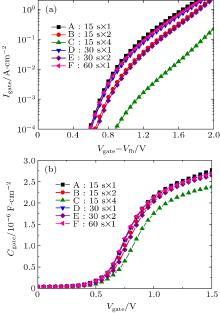
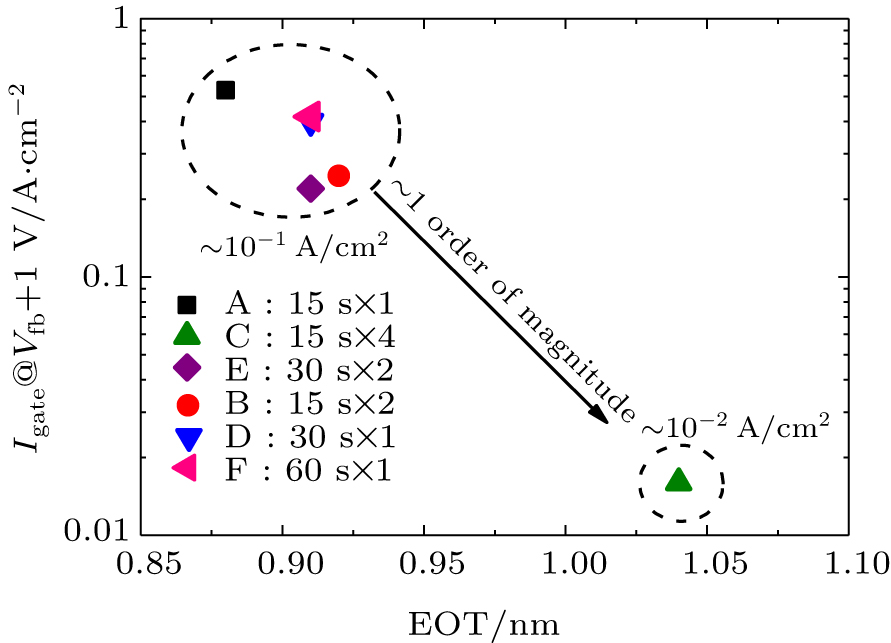
Influence of multi-deposition multi-annealing on time-dependent dielectric breakdown characteristics of PMOS with high- k/metal gate last process*
Wang Yan-Rong, Yang Hong, Xu Hao, Wang Xiao-Lei, Luo Wei-Chun, Qi Lu-Wei, Zhang Shu-Xiang, Wang Wen-Wu, Yan Jiang, Zhu Hui-Long, Zhao Chao, Chen Da-Peng, Ye Tian-Chun
Key Laboratory of Microelectronics Devices and Integrated Technology, the Institute of Microelectronics, Chinese Academy of Sciences, Beijing 100029, China

Corresponding author. E-mail: wangwenwu@ime.ac.cn

*Project supported by the National High Technology Research and Development Program of China (Grant No. SS2015AA010601) and the National Natural Science Foundation of China (Grant Nos. 61176091 and 61306129).

Abstract

A multi-deposition multi-annealing technique (MDMA) is introduced into the process of high- k/metal gate MOSFET for the gate last process to effectively reduce the gate leakage and improve the device’s performance. In this paper, we systematically investigate the electrical parameters and the time-dependent dielectric breakdown (TDDB) characteristics of positive channel metal oxide semiconductor (PMOS) under different MDMA process conditions, including the deposition/annealing (D&A) cycles, the D&A time, and the total annealing time. The results show that the increases of the number of D&A cycles (from 1 to 2) and D&A time (from 15 s to 30 s) can contribute to the results that the gate leakage current decreases by about one order of magnitude and that the time to fail (TTF) at 63.2% increases by about several times. However, too many D&A cycles (such as 4 cycles) make the equivalent oxide thickness (EOT) increase by about 1 Å and the TTF of PMOS worsen. Moreover, different D&A times and numbers of D&A cycles induce different breakdown mechanisms.

Keyword: 73.40.Qv; 77.55.D–; 85.30.Tv; high- k/metal gate; time dependent dielectric breakdown; multi-deposition multi-annealing
1. Introduction

With the scaling down of the metal– oxide– semiconductor field-effect transistor (MOSFET), the high-k/metal gate (HKMG) has become more popular for CMOS integration process beyond the 45-nm node.[1] As is well known, the HKMG last process is necessary for the 22-nm node and beyond, which has been widely applied in manufactoring.[2] However, because of the small thermal budget in the gate-last process, there are many traps and defects in the gate stack, which induce large leakage and worse reliability issues, such as time-dependent dielectric breakdown (TDDB), bias temperature instability (BTI), and hot carrier injection (HCI). So, post deposition annealing (PDA) has become more important to solve this problem.[3] A novel PDA technique, the multi-deposition multi-annealing (MDMA) technique, was proposed and estimated.[4, 5] However, there has not been enough systematic analysis about the influence of the MDMA on the TDDB characteristics, especially for the gate-last process. Moreover, TDDB, as one of the most important reliability issues, [6] is widely concerned and will be more important for the beyond 22-nm node.[7] In this paper, we study the electrical and TDDB characteristics of HKMG gate-last PMOS with different MDMA techniques, including the number of deposition/annealing (D& A) cycles and the D& A time. Moreover, the TDDB breakdown mechanism is also analyzed.

2. Devices and experiments

In this study, the SiO2/HfO2/TiN gate stack was fabricated on (100) n-type Si wafer by gate-last process. The interface layer (IL) was grown using the O-zone method after cleaning the silicon surface, and the HfO2 films were deposited by atomic layer deposition (ALD) using the MDMA technique (annealing at 450  ° C and with different annealing times). Six different samples were prepared: the D& A cycles of samples A, D, and F were 1, and their annealing times were 15  s, 30  s, and 60  s respectively; the numbers of D& A cycles of samples B and E were 2, and their annealing times of each cycle were 15  s and 30  s respectively; for sample C, its annealing time was 15  s and the number of D& A cycles was 4, which was marked as 15  s × 4. The total ALD cycles of each sample were kept constant as shown in Table  1. Then 4-nm TiN was deposited by ALD. Here, the electrical and TDDB characteristics were measured with a Keithley 4200, and TDDB was tested by using constant voltage stress (CVS) at high field. The area of MOSCAP was 2.5 × 10− 5  cm2.

Table 1. Six samples fabricated by MDMA technique.
3. Results and discussion
3.1. Basic electrical characteristics.

Figure  1 shows the basic electrical characteristics of the p-MOSCAPs used in the experiments. Figure  2 shows the relations between the gate leakage and the equivalent oxide thickness (EOT) of these six samples. Here, the characteristics of sample C are quite different from those of the other samples. The EOT of sample C is 0.1  nm larger than that of the other samples, while the gate leakage is 1 order of magnitude smaller than the other samples’ at gate voltage Vfb + 1  V. In other words, increasing the number of D& A cycles reduces the gate leakage, however, more D& A cycles (four cycles) induce EOT to increase.

Fig.  1. (a) The IgVg characteristics and (b) CgVg characteristics of p-MOSCAPs.

Fig.  2. Relation between gate leakage and EOT of the samples with different numbers of D& A cycles or D& A times.

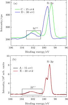
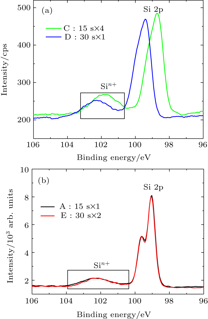
For the same total high-k deposition (∼ 2.4  nm), the more the D& A cycles are, the thinner the high-k layer for each D& A cycle is. For sample C, the first annealing occurs so closer to the interfacial layer than the others that the oxygen atoms enter into IL to increase the thickness of the IL and induce a small gate leakage. When the number of D& A cycles is large enough, the MDMA induces EOT to increase greatly and gate leakage to reduce greatly. The phenomenon is due to the IL growth. This can be demonstrated by the x-ray photoelectron spectroscopy (XPS) experiment shown in Fig.  3. Comparing Sin+ /Si of samples C and D, it can be concluded that the amount of Sin+ in sample C is much higher than that in sample D. Similarly, sample A has a much higher amount of Sin+ /Si than sample E according to the XPS results. Therefore it can be demonstrated that increasing the number of D& A cycles can improve the quality of the IL.

Fig.  3. Si  2p XPS spectra of HfO2/IL/Si stack. Peak positions are all assigned to C  1s peak binding energy. The results in panels (a) and (b) are obtained using different equipments.

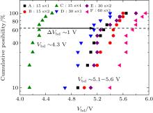
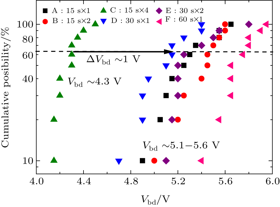
3.2. Time zero dielectric breakdown characterization.

The time zero dielectric breakdown (TZDB) as shown in Fig.  4 is measured. The dielectric breakdown voltage (Vbd) is defined as the voltage at which the current increases by about one order of magnitude. In Fig.  4, the TZDB voltage of sample C is 4.3  V, while the TZDB voltages of the other samples are about 5.1– 5.4  V. Sample C is the worst one. In order to know more about the breakdown characteristics of these samples, we analyze the TDDB characteristics and the physical mechanism.

Fig.  4. Cumulative possibilities of breakdown voltage.

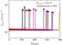
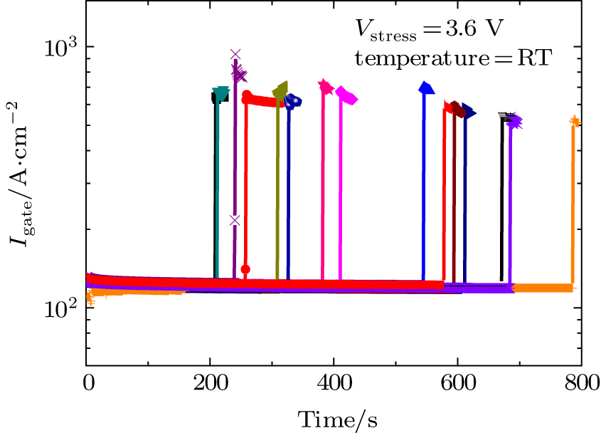
3.3. Time dependent dielectric breakdown characteristics.

A constant voltage stress of 3.6  V is applied to several fresh MOSCAPs of each sample. These experiments are carried out at room temperature. The current increases slightly until hard breakdown occurs. There are no significant soft breakdowns before the hard breakdowns take place. In this paper, the 0.5Ig increase is defined as the failure criterion. Figure  5 shows the breakdown characteristics of the MOSCAP.

Fig.  5. Breakdown characteristics of the MOSCAP, with 0.5Ig increase being the failure criterion.

In Fig.  6(a), we can obtain the TTFs of samples A, D, and F at the failure percentile of 63.2%. By comparing the TTFs, it can be concluded that doubling the PDA time can double the TTF. The reason is probably that increasing the annealing time can improve the quality of the HK layer by reducing the oxygen vacancies in the HK layer. This is proved by comparing the O 1s densities/Hf 4f densities of samples A and E acquired from the XPS experiment. The O 1s and Hf 4f densities of sample A are less than those of sample E. (The fitting results are not shown in this article.) What is more, the gate leakage current has decreased. The Weibull distributions of samples A, B, C, and E are shown in Fig.  6(b). For samples A, B, and C, the annealing time of each cycle is 15  s, whereas the annealing cycles of them are quite different: the number of cycles of sample C is 4, four times that of A, and the number of annealing cycles of B is two. In Fig.  6(b), it can be seen that the TTF of B is ten times more than that of sample C and it is also about five times that of sample A. The conclusion is that properly increasing the number of PDA cycles can improve the quality of the devices, however when the number of PDA cycles is too many, the quality of the IL is affected, which can lead to the decrease of lifetime. As for samples D and E, the number of annealing cycles increased from 1 to 2 can cause the TTF to become ten times longer.

Fig.  6. Weibull distribution of HfO2 gate stack MOSCAP tested under Vg = 3.6  V at room temperature, showing (a) the weibull distribution of samples with only one D& A cycle and (b) the weibull distribution of samples with multi D& A cycles.

The slope of the Weibull distribution, β , is an important parameter to evaluate the reliability properties. There is the transition of the Weibull slope as shown in Fig.  6, and the slopes of these six samples are different (Table  2), which means the crucial layers that determine breakdowns are different. Generally, the Weibull slope β is dependent on the thicknesses of high-k and IL.[8] The β of the IL (0.8  nm) is about 1, and that of the HK layer is almost the same value 1.5– 2.0.[9] It is the IL that determines the breakdown for sample A, and for the low percentile sample D, the breakdown is mainly caused by the IL. However, the HK layer determines the breakdown for the high percentile sample D. As for sample C, it is the HK layer that controls the breakdown. This is in accordance with the case of the low gate leakage current of sample C. This means that both the number of PDA cycles and PDA time of each cycle can determine the main breakdown layer. The reason has been demonstrated by the XPS experiment shown in Fig.  3.

Table 2. Slopes of bimodal distribution.

It can be properly concluded that increasing the number of annealing cycles can also improve the quality of the HK layer by reducing the oxygen vacancies, but too many cycles can lead to the oxygen vacancies entering into IL, which has been proven by the XPS experiment. The increasing of the IL thickness leads to smaller leakage current and shorter lifetime.

4. Conclusion

The MDMA technique for HKMG gate-last process can reduce the gate leakage and affect the TDDB characteristics and the degradation mechanism. Properly increasing the annealing time and the number of annealing cycles can reduce the oxygen vacancies in the HK layer. In our study, changing the annealing time from 15  s to 30  s can reduce the gate leakage current by 15% and increase the lifetime by 34%. Increasing the number of annealing cycles from 1 to 2 can reduce the gate leakage current by twice and increase the lifetime by 8 times. Even though too many annealing cycles lead to small gate leakage current and large EOT due to the increased IL during PDA, but they induce worse TTF of TDDB due to worse HK layer by HK-breakdown mechanism.

Reference
1 Wilk G D, Wallace R M and Anthony J M 2001 J. Appl. Phys. 89 5243 DOI:10.1063/1.1361065 [Cited within:1]
2 Matsuki T, Toni K, Maeda T, Syoji H, Kiyono K, Akasaka Y, Hayashi K, Kasai N and Arikado T 2004International Conference on Microelectronic Test Structures 17 105 DOI:10.1109/ICMTS.2004.1309310 [Cited within:1]
3 Cartier E, Hopstaken M and Copel M 2009 Appl. Phys. Lett. 95 042901 DOI:10.1063/1.3186075 [Cited within:1]
4 Nabatame T, Iwamoto K, Ota H, Tominaga K, Hisamatsu H, Yasuda T, Yamamoto K, Mizubayashi W, Morita Y, Yasuda N, Ohno M, Horikawa T and Toriumi A 2003IEEE VLSI Symp. 25 DOI:10.1109/VLSIT.2003.1221068 [Cited within:1]
5 Wu L, Yew K S, Ang D S, Liu W J, Le T T, Duan T L, Hou C H, Yu X F, Lee D Y, Hsu K Y, Xu J, Tao H J, Cao M and Yu H Y 2010 IEEE International Electron Devices Meeting 273 DOI:10.1109/IEDM.2010.5703343 [Cited within:1]
6 Hirano I, Nakasaki Y, Fukatsu S, Goto M, Nagatomo K, Inumiya S, Sekine K, Mitani Y and Yamabe K 2013 Microelectronics Reliability 53 1868 DOI:10.1016/j.microrel.2013.05.010 [Cited within:1]
7 Ramey S, Ashutosh A, Auth C, Clifford J, Hattendorf M, Hicks J, James R, Rahman A, Sharma V, St Amour A and Wiegand C 2013IEEE Inrenational Reliability Physics Symposium 4C51 DOI:10.1109/IRPS.2013.6532017 [Cited within:1]
8 Nigam T, Kerber A and Peumans P 2009IEEE International Reliability Physics Symposium 523 DOI:10.1109/IRPS.2009.5173307 [Cited within:1]
9 Stathis J H, Wang M, Southwick R G, Wu E Y, Linder B P, Liniger E G, Bonilla G and Kothari H 2014 IEEE International Electron Devices Meeting 522 DOI:10.1109/IEDM.2014.7047091 [Cited within:1]