Yang Ming, Lin Zhao-Jun, Zhao Jing-Tao, Wang Yu-Tang, Li Zhi-Yuan, Lv Yuan-Jie, Feng Zhi-Hong. Improvement of switching characteristics by substrate bias in AlGaN/AlN/GaN heterostructure field effect transistors* . Chinese Physics B, 24(11): 117103
Permissions
Improvement of switching characteristics by substrate bias in AlGaN/AlN/GaN heterostructure field effect transistors*
Yang Minga),b), Lin Zhao-Juna), Zhao Jing-Taoa), Wang Yu-Tanga), Li Zhi-Yuana), Lv Yuan-Jieb), Feng Zhi-Hongb)
School of Physics, Shandong University, Jinan 250100, China
National Key Laboratory of Application Specific Integrated Circuit (ASIC), Hebei Semiconductor Research Institute, Shijiazhuang 050051, China
*Project supported by the National Natural Science Foundation of China (Grant Nos. 11174182 and 61306113) and the Specialized Research Fund for the Doctoral Program of Higher Education, China (Grant No. 20110131110005).
Abstract
A simple and effective approach to improve the switching characteristics of AlGaN/AlN/GaN heterostructure field effect transistors (HFETs) by applying a voltage bias on the substrate is presented. With the increase of the substrate bias, the OFF-state drain current is much reduced and the ON-state current keeps constant. Both the ON/OFF current ratio and the subthreshold swing are demonstrated to be greatly improved. With the thinned substrate, the improvement of the switching characteristics with the substrate bias is found to be even greater. The above improvements of the switching characteristics are attributed to the interaction between the substrate bias induced electrical field and the bulk traps in the GaN buffer layer, which reduces the conductivity of the GaN buffer layer.
AlGaN/GaN heterostructure field effect transistors (HFETs) have been demonstrated to be extremely promising for various applications, such as high power, high frequency, high temperature, and switching power devices.[1– 7] For the switching applications, a low OFF-state power loss, a high ON/OFF current ratio, and a low subthreshold swing are considerably critical.[8– 11] To improve the switching characteristics of AlGaN/GaN HFETs, many different approaches were proposed, for example, O2 plasma treatment, oxide-filled isolation structure followed by N2/H2 postgate annealing, dry etching cap layer, and using high-k gate insulator materials.[8– 11] However, almost all of the approaches have disadvantages: structure damages, ON-state current reduction, or gate modulating ability degradation. So, to develop an approach which can improve the switching characteristics without structure damaging and, at the same time, keep the ON-state current as large as possible is essentially important.
In this paper, a simple and effective approach to reduce the OFF-state current and, meanwhile, keep the ON-state current constant in AlGaN/AlN/GaN HFETs by a substrate bias is presented. With this approach, the ON/OFF current ratio and the subthreshold characteristics are enhanced by a large margin.
2. Experiments
As shown in Fig. 1, the AlGaN/GaN heterostructure with an AlN interlayer was grown on a 420-μ m thick c-plane sapphire substrate by metal-organic chemical vapor deposition (MOCVD), which consisted of (from bottom) a 40-nm AlN nucleation layer, a 1.5-μ m undoped GaN buffer layer, a 0.5-nm undoped AlN interlayer, and a 22.5-nm undoped Al0.28Ga0.72N barrier layer. A typical AlGaN/AlN/GaN HFET was fabricated as follows. Firstly, the mesa isolation was formed by Cl2/BCl3 plasma. Then, the source and the drain Ohmic contacts both with the dimensions of 50 μ m× 50 μ m (length × width) were formed by Ti/Al/Ni/Au deposition and rapid thermal annealing at 800 ° C for 30 s in N2 ambient. The distance between the drain and the source was 5 μ m (Fig. 1). Via transmission line method (TLM) patterns, 0.60 Ω · mm Ohmic contact resistance was obtained. Subsequently, a Ni/Au contact was deposited between the source and the drain to form the Schottky gate. The gate Schottky contact was rectangular with a length of 1 μ m and a width of 50 μ m, and the distance between the gate and the source was 1 μ m. After the fabrication of the transistor, the Ni/Au (60 nm/160 nm) contact was deposited directly on the back of the substrate as an electrode to apply a substrate bias. Different voltage biases were applied on the substrate when the current– voltage (I– V) curves were measured by an Agilent B1500A semiconductor parameter analyzer at room temperature. Then, 300 μ m thickness of the sapphire substrate was ground off. Similarly, the Ni/Au contact was deposited on the back of the thinned substrate to apply various voltage biases for the I– V character measurements.
Fig. 1. Schematic cross section of the fabricated AlGaN/AlN/GaN HFET with the deposited substrate metal (Ni/Au) electrode.
3. Results and discussion
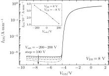
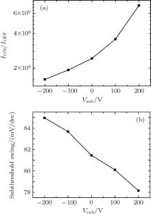
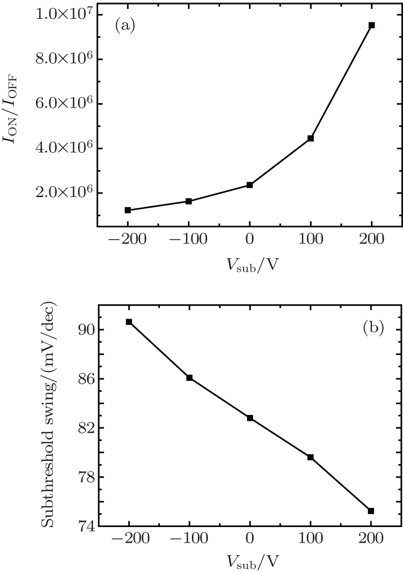
Figure 2 shows the measured drain-to-source current IDS as a function of gate-source bias VGS under drain-source bias VDS = 8 V and different substrate voltage biases Vsub. The inset shows IDS as a fuction of Vsub at VDS = 8 V and VGS = − 8 V. From this figure, it is found that the OFF-state current becomes several times smaller with the increase of Vsub (nearly deceasing linearly from 3.77 A/mm at Vsub = − 200 V to 1.11 A/mm at Vsub = 200 V), and the ON-state current keeps constant. Consequently, the ON/OFF drain current ratio (ION/IOFF) at Vsub = 200 V becomes several times larger than that at Vsub = 0 V, as shown in Fig. 3(a). The subthreshold swing becomes smaller by a certain degree with the increase of Vsub, which is shown in Fig. 3(b). It demonstrates an improvement of the switching characteristics by a positive substrate bias in the AlGaN/AlN/GaN HFET.
Fig. 2. Measured IDS at VDS = 8 V as a function of VGS under different substrate voltage biases Vsub. The inset shows IDS as a fuction of Vsub at VDS = 8 V and VGS = − 8 V.
Fig. 3. (a) ON/OFF drain current ratio ION/IOFF and (b) subthreshold swing variations with Vsub. Both of them demonstrate an improvement of switching characteristics with the increase of the substrate bias.
This phenomenon can be explained as follows. In AlGaN/GaN HFETs, the OFF-state drain current mainly consists of three parts: the gate leakage current (IG), the drain-to-source leakage current flowing through the GaN buffer layer (Ibuff), and the drain-to-substrate leakage current (Isub) in the vertical direction.[12] The natural insulation of the sapphire substrate prevents the current flowing in the vertical direction, so Isub is negligible.[13] The electric field induced by the substrate bias is in the vertical direction, and the influence of the substrate bias is confined in the space below the two-dimensional electron gas (2DEG).[14] Moreover, between IG and Ibuff, Ibuff is always preferential.[13] As a result, the variation of the OFF-state current would be attributed to the variation of Ibuff with Vsub. Moreover, Ibuff is closely related with the bulk traps in the GaN buffer layer.[12] The buffer traps (donor traps or acceptor traps) arise from crystalline defects, such as point defects, threading dislocations, Ga vacancies, and background donor doping (such as Si and O).[12, 13] The electric field (∼ 5 × 10³ V/cm at Vsub = 200 V) induced by the substrate bias would interact with these traps, inducing the ionization or deionization of the GaN buffer traps.[12] The ionization of the acceptor traps would deplete the electrons in the buffer layer, which originate from the ionization of the donor traps.[12] From Fig. 2, with positive Vsub, the ionization of the acceptor traps and (or) the deionization of the donor traps would play a more important role, leading to a decrease of Ibuff and thus the lower OFF-state drain current.[12] What is more, the positive Vsub would tend to drive the electrons to the bottom portion of the buffer layer, and the holes to the top. At the bottom portion of the buffer layer, the defect density is much larger, so the electron mobility will be much lower. Another possibility is that the electrons are driven into the AlN nucleation layer. Since this layer has a larger resistivity, the leakage current will be further reduced. As for the ON-state case, the 2DEG channel under the gate is open, and IDS is dominated by the gate bias.[15] The influence of the ionization/deionization of the GaN buffer traps induced by Vsub is not remarkable, compared with so much larger IDS. So, the ON-state current keeps constant whatever Vsub is, and the switching characteristics are improved.
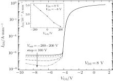
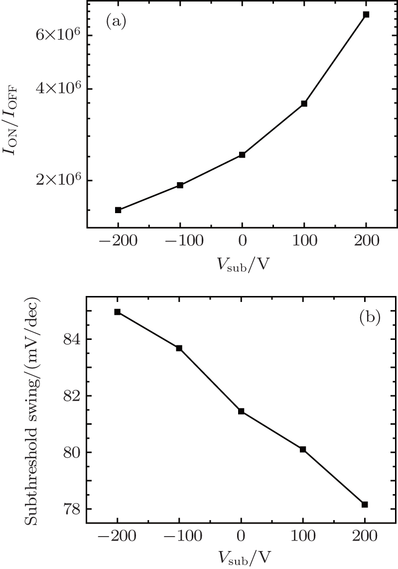
To explore more about the influence of the substrate bias, the 420 μ m sapphire substrate was thinned to 120 μ m by grinding, and a similar measurement procedure was carried out. Figure 4 shows the measured IDS at VDS = 8 V as a function of VGS under different substrate voltage biased Vsub. Compared with the original situation, it follows a similar trend, but the variations of the OFF-state current become more remarkable, which can also be seen from the inset showing IDS as a function of Vsub at VDS = 8 V and VGS = − 8 V. The OFF-state current changes from 2.6 × 10− 7 A/mm at Vsub = 0 V to 3.4 × 10− 8 A/mm at Vsub = 200 V, corresponding to a reduction by almost one order of magnitude. The ON-state current still keeps constant, so the ON/OFF drain current ratio is enhanced by nearly one order of magnitude, i.e., from 2.4 × 10⁶ at Vsub = 0 V to 9.5 × 10⁶ at Vsub = 200 V, as shown in Fig. 5(a). Figure 5(b) indicates the subthreshold swing as a function of Vsub. It changes from 82.8 mV/dec at Vsub = 0 V to 75.2 mV/dec at Vsub = 200 V. It means that, from Vsub = 0 V to Vsub = 200 V, the switching characteristics of the device with the thinned substrate improve more than that of the original one. This is attributed to the larger electric field induced by Vsub (∼ 2 × 10⁴ V/cm at Vsub = 200 V) with the thinner substrate, and thus the stronger interaction between the electric field and the GaN buffer traps.[12] The electric field induced by 200 V Vsub for the 120 μ m substrate is equivalent to the electric field induced by 700 V Vsub for the 420 μ m substrate. It means that, for the original device (with 420 μ m substrate), the trend of switching characteristic improvement is still available in a larger Vsub range (∼ 700 V).
Fig. 4. For 300 μ m thinned substrate, the measured IDS at VDS = 8 V as a function of VGS under different substrate voltage biases Vsub. The inset shows IDS at VDS = 8 V and VGS = − 8 V as a fuction of Vsub. Comparing with the original one (Fig. 2), the influence of the substrate bias becomes greater.
Fig. 5. For 300 μ m thinned substrate, (a) ON/OFF drain current ratio ION/IOFF and (b) subthreshold swing variations with Vsub. Both of them demonstrate a greater improvement of switching characteristics with the increase of the substrate bias.
4. Conclusion
A simple and effective approach to improve the switching characteristics in AlGaN/AlN/GaN HFETs by applying a voltage bias on the sapphire substrate has been proposed. With this approach, the OFF-state drain current is much reduced and the ON-state current keeps constant. As a result, the ON/OFF drain current ratio is enhanced by a large margin and the corresponding subthreshold swing is decreased. The improvement of the switching characteristics arises from the interaction between the electric field induced by the substrate voltage bias and the GaN buffer traps. Moreover, with the thinned substrate, the improvement of the switching characteristics becomes much greater compared to the original one (without substrate thinning).
ZhaoJ, LinZ, CorriganT D, WangZ, YouZ and WangZ2007Appl. Phys. Lett. 91173507DOI:10.1063/1.2798500[Cited within:1]
1
2005
0.0
0.0
... [1#cod#x2013 ...
1
2011
0.0
0.0
1
2015
0.0
0.0
1
2001
0.0
0.0
1
2015
0.0
0.0
1
2014
0.0
0.0
1
2014
0.0
0.0
... 7] For the switching applications, a low OFF-state power loss, a high ON/OFF current ratio, and a low subthreshold swing are considerably critical ...
2
2008
0.0
0.0
... [8#cod#x2013 ...
... [8#cod#x2013 ...
1
2010
0.0
0.0
1
2012
0.0
0.0
2
2013
0.0
0.0
... 11] To improve the switching characteristics of AlGaN/GaN HFETs, many different approaches were proposed, for example, O2 plasma treatment, oxide-filled isolation structure followed by N2/H2 postgate annealing, dry etching cap layer, and using high-k gate insulator materials ...
... 11] However, almost all of the approaches have disadvantages: structure damages, ON-state current reduction, or gate modulating ability degradation ...
7
2014
0.0
0.0
... [12] The natural insulation of the sapphire substrate prevents the current flowing in the vertical direction, so Isub is negligible ...
... [12] The buffer traps (donor traps or acceptor traps) arise from crystalline defects, such as point defects, threading dislocations, Ga vacancies, and background donor doping (such as Si and O) ...
... [12,13] The electric field (#cod#x223C ...
... [12] The ionization of the acceptor traps would deplete the electrons in the buffer layer, which originate from the ionization of the donor traps ...
... [12] From Fig ...
... [12] What is more, the positive Vsub would tend to drive the electrons to the bottom portion of the buffer layer, and the holes to the top ...
... [12] The electric field induced by 200 V Vsub for the 120 #cod#x03BC ...
3
2013
0.0
0.0
... [13] The electric field induced by the substrate bias is in the vertical direction, and the influence of the substrate bias is confined in the space below the two-dimensional electron gas (2DEG) ...
... [13] As a result, the variation of the OFF-state current would be attributed to the variation of Ibuff with Vsub ...
... [12,13] The electric field (#cod#x223C ...
1
2003
0.0
0.0
... [14] Moreover, between IG and Ibuff, Ibuff is always preferential ...
1
2007
0.0
0.0
... [15] The influence of the ionization/deionization of the GaN buffer traps induced by Vsub is not remarkable, compared with so much larger IDS ...
Improvement of switching characteristics by substrate bias in AlGaN/AlN/GaN heterostructure field effect transistors*
[Yang Minga),b), Lin Zhao-Juna), Zhao Jing-Taoa), Wang Yu-Tanga), Li Zhi-Yuana), Lv Yuan-Jieb), Feng Zhi-Hongb)]


 , Zhao Jing-Tao