†Corresponding author. E-mail: canhualiu@sjtu.edu.cn
Corresponding author. E-mail: jfjia@sjtu.edu.cn
*The work in SJTU was supported by the National Basic Research Program of China (Grant Nos. 2013CB921902 and 2011CB922200) and the National Natural Science Foundation of China (Grant Nos. 11227404, 11274228, 11521404, 11174199, and 11134008).
The discovery of an extraordinarily superconductive large energy gap in SrTiO3 supported single-layer FeSe films has recently initiated a great deal of research interests in surface-enhanced superconductivity and superconductive ultrathin films fabricated on crystal surfaces. On account of the instability of ultra-thin films in air, it is desirable to perform electrical transport measurement in ultra-high vaccum (UHV). Here we review the experimental techniques of in situ electrical transport measurement and their applications on superconductive ultrathin films.
Recently, the discovery of single-layer FeSe films grown on SrTiO3(001) (FeSe/STO) with a potential critical temperature (Tc) of ∼ 80 K, [1] which is nearly ten times the Tc of bulk FeSe and higher than the record value of 56 K for known bulk Fe-based superconductors at ambient atmosphere, [2] raised the hope to obtain ultrahigh-Tc superconductivity in ultrathin films irrespective of their susceptibility to quantum phase fluctuations. Although the large superconductive-like energy gap firstly observed on FeSe/STO by scanning tunneling spectroscopy (STS) was soon confirmed by angle-resolved photoemission spectroscopy (ARPES), [3, 4] rigorous verification of the high-Tc superconductivity requires experimental observations of both zero resistance and Meissner effect. In traditional four-electrode transport measurement, samples have to be exposed to atmosphere for fabrication of electrodes, which is easy to bring damage to the ultrathin samples. Therefore, in previous ex situ electrical transport measurements, [5– 7] several layers of FeTe thin film and an amorphous Si film were deposited on the FeSe/STO surface for protection. The Si/FeTe/FeSe/STO system shows zero resistance at a temperature no more than 23.5 K, which is higher than bulk FeSe at ambient atmosphere but much lower than the expectation. In contrast, without taking the single-layer FeSe films out from ultra-high vacuum (UHV), Ge et al. performed electrical transport measurements with a self-developed four-point probe (4PP).[8] They found that the zero resistance of FeSe/STO sustains above 100 K. These experiments well demonstrated the importance of in situ electrical transport measurements for the study of superconductive ultrathin films.
The merit of in situ measurement is obvious: sample quality can be maximally kept for acquiring their intrinsic physical properties. However, in situ electrical transport measurement has not been so widely applied yet in the research field of superconductivity, possibly due to the fact that fascinating but air-sensitive superconductive ultrathin films were discovered only recently. Besides single-layer FeSe/STO films, single atomic layers of Pb and In grown on Si(111)-7 × 7 surfaces have also been observed to show superconductive transition in in situ electrical transport measurements, and their Tc’ s are comparable to those of their bulk materials.[9– 12]
To develop an instrument for in situ electrical transport measurement, efforts must be made to ensure that electrodes should be electrically well connected with the sample surface, while not bringing severe damage to it. A multiple-probe (MP) STM is therefore a very suitable technique, [13, 14] since its probes, i.e., electrodes, can be precisely controlled to touch a sample surface without severe contact damage. So far, however, no MP STM has been applied to studies of superconductive films yet, although its ability for in situ electrical transport measurement has been demonstrated in many other lowdimensional materials.[15– 20] Here, we focus on other three in situ electrical transport measurement systems that have been utilized to study superconductive ultrathin films.
Nanostenciling is a widely used technique for producing nanostructures on a substrate by vacuum deposition through a shadow mask.[21, 22] Uchihashi and colleagues have used it to fabricate clean electrodes for measuring electrical transport properties of atomically thin nanowires grown on silicon single-crystal surfaces on an UHV machine equipped with STM.[23] Comparing with conventional photo/electron-beam lithography, nanostenciling is more suitable for fabrication of electrodes in UHV due to its simpler and contaminator-free operation process.
Figure 1(a) is a schematic illustration of the nanostenciling setup. A free-standing shadow mask made of a 2-μ m-thick titanium foil is brought to contact with sample surface. Pure metal atoms, e.g., Ag, Au, Pb, etc, are evaporated from an evaporator and only those getting through the hole pattern in the shadow mask can be absorbed and form desired nanostructures, i.e., electrodes and markers, on the sample surface, as shown in Fig. 1(b). All through holes were fabricated by focused ion beam. In Uchihashi et al.’ s experiment, [23] atomically thin nanowires were grown on the sample surface after the preparation of electrodes. The STM was used to observe the quality of the nanowires and their connection with electrodes, as shown in Fig. 1(c). It is revealed in the STM image that there are three nanowires, 0.6– 1.0 nm in height and 3– 8 nm in width, bridge the electrode gap, as indicated by the arrows.
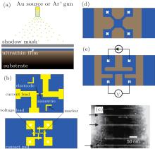 | Fig. 1. (a) Schematic illustration of a nanostenciling setup. Yellow spots represent Au atoms (Ar+ ions) evaporated (sputtered) from a Au source (Ar+ gun). (b) Schematic drawing of electrode patterning fabricated by nanostenciling. It is used for in situ two-terminal transport measurement of nanowires. Upper: close up around the center; lower: overview. (c) STM image of two electrodes connected with ErSi2 nanowires. The arrows indicate the nanowires bridging the electrode gap.[23] (d), (e) Schematic drawing of sample patterning in Van der Pauw’ s and linear configurations, respectively, for in situ four-terminal transport measurement of superconductive ultrathin films. Blue areas are the  |
For 2D ultrathin film samples, there is no need to perform high-resolution nanostenciling. A shadow mask having a desired through-hole pattern with a resolution of sub-millimeter would be enough for fabrication of a four-electrode patterning, as shown in Figs. 1(d) and 1(e). In both figures, blue areas are pre-prepared superconductive ultrathin film, the 


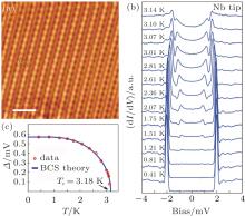 | Fig. 2. Discovery of superconductivity in the surface of    |
The first direct evidence of zero resistance of the 

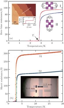 | Fig. 3. Transport experimental evidence for the superconductivity of the   |
As it is convenient to change shadow masks, it is possible to take different measurement configurations by designing various through-hole patterns. Van der Pauw’ s measurements are useful for checking the anisotropy of electron conduction and to exclude the possibility of spurious supercurrents. To have a uniform spatial distribution of bias current, Uchihashi et al. adopted a measurement configuration with a linear current path between voltage terminals, as shown in Fig. 1(e) and inset of 3(c).[11] Results from two 
It is worth noting that when bringing spring probes into contact with the current– voltage terminal patterns on a sample surface, one needs the help of an optical microscope. It is thus difficult to install a closing coil surrounding the sample for applying an external magnetic field in Uchihashi’ s present apparatus. This problem is circumvented by using an assembled four-point probe to be introduced below.
This year is happened to be the 100th anniversary of the four-point probe technique, which was firstly introduced by Frank Wenner and nowadays has become an interdisciplinary characterization tool in materials science, semiconductor industries, geology, physics, etc.[27] Measuring the electrical transport property of a two-dimensional (2D) sheet with a 4PP was well analyzed in theory by Smits nearly 60 years ago.[28] The primarily considered measurement configurations are shown in Fig. 4. Four tips are linearly arranged on a sheet film, and the position of the i-th tip is denoted as ri with the relation of r4 > r3 > r2 > r1. Figure 4(a) shows the measurement configuration C1423, in which current I is applied through the outer two tips, 1 and 4, and the voltage drop V is measured between the inner two tips, 2 and 3. In another measurement configuration C1234, current and voltage electrodes are tip pairs of (1, 2) and (3, 4), respectively, as shown in Fig. 4(b). In the case of a uniform infinite 2D film, the resistance measured in the two configurations is given by[29, 30]
 |
 |
Here, Rs is the sheet resistivity of the 2D film. In case that the tip spacing is identical, i.e., r4 − r3 = r3 − r2 = r2 − r1, the measured resistance in the two measurement configurations can be simplified to be
 |
 |
 | Fig. 4. Schematic illustration of 4PP measurement in linear configurations of (a) C1423 and (b) C1234. |
It is worth mentioning that it is always difficult to have equal tip spacings or to keep tip spacings unchanged in a series of measurement in practice. It is therefore necessary to measure both R1423 and R1234 so as to get Rs by using the following equation deduced from Eqs. (1) and (2):
 |
With this equation, positional error along the line is totally eliminated[31] and off-line positional errors influence the measurement only as a second-order effect.[32] Equation (5) is actually very important for analyzing 4PP experimental data, as demonstrated in Yamada et al.’ s experiments[33] introduced below.
Most of 2D films need to be supported by a substrate, which is not always insulating. In such cases, a 4PP with smaller tip spacing would be more desirable for transport measurement. Hasegawa and collogues made the pioneering work in developing in situ micro-4PP measurement systems, [33– 37] in which the tip spacing is down to several μ m. Figure 5(a) is an scanning electron microscopy (SEM) image of the top part of a micro-4PP unit, which was made by using silicon-based microfabrication technology. Its fabrication procedure is very similar to that of an atomic-force microscope tip.[34, 35] The micro-4PP has four metal-coated silicon oxide cantilevers, i.e., tips, extending from a silicon support chip that is fixed on a ceramic substrate, as schematically shown in Fig. 5(c).[35]
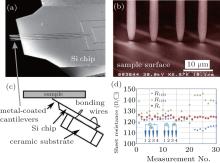 | Fig. 5. Implement of micro-4PP.[33– 36] (a) SEM image of micro-4PP consisting of four metal-coated cantilevers that are supported on a Si chip (courtesy by S. Hasegawa). (b) SEM image of micro-4PP with tops of four cantilevers contacting a Si(111) surface (courtesy by S. Hasegawa). (c) Schematic illustration of the side view of micro-4PP contacting a sample surface. (d) Sheet resistance measured at room temperature on a ∼ 20-bilayer Bi(111) film grown on Si(111)-7 × 7 substrate with both measurement configurations C1423 and C1234. The measurements were performed 30 times by repeating cycles of detaching/touching probes from/to the sample surface. Rs was extracted from Eq. (5). |
The micro-4PP was mounted on a piezo-activated probe stage whose movement can be precisely controlled in three dimensions with an accuracy of about 10 nm.[35] Because the micro-4PP tips are flexible and approach sample surfaces in an inclined angle, they can make contacts with sample surfaces straightforward even when the surface plane is not aligned with the tip tops, as shown in Fig. 5(b). It is worth mentioning that the tips are so flexible that they are easily bent laterally as well as longitudinally by contact, resulting in unequal tip spacings. Therefore, the measured 4PP resistance in both measurement configurations, i.e., R1423 and R1234, usually show scattered values among different contacts, as obtained on Bi(111) thin film (about 20 bilayer thick) grown on a Si(111)-7 × 7 substrate and shown in Fig. 5(d). In contrast, the scattering of Rs values deduced from Eq. (5) is significantly suppressed, which thus demonstrated well the feasibility of the micro-4PP electrical transport measurement.
Thermally connecting sample and probe stages to a liquid N2/He tank, Tanikawa et al. developed a UHV instrument for variable-temperature in situ micro-4PP electrical transport measurement, in which the approach of 4PP to sample surfaces can be monitored by an optical microscope.[37] The utility of in situ 4PP has been well demonstrated in previous measurements of surface conductivity of various superstructures prepared on Si(111) surfaces, in which novel physical phenomena correlated with electrical transport properties of 2D electronic systems have been well studied.[16, 25, 36, 38, 39] Furthermore, Yamada et al. have recently developed a new micro-4PP measurement system that can be conducted at sub-kelvin temperature and under high perpendicular magnetic field in UHV.[33] The key part of the micro-4PP unit is basically the same as that developed by Tanikawa et al., although necessary modification was done on probe stage. The main advancement of the newly developed micro-4PP measurement apparatus is the utilization of a superconductor magnet that is immersed in liquid helium, as shown in Fig. 6(a). Since the measuring head consisting of 4PP and sample stages is set in the bottom of an insert chamber and surrounded by the superconductor magnet, it is only possible to approach the 4PP to sample surfaces in blind. Later practice confirmed that the blind approach also works well.
With the newly developed micro-4PP measurement apparatus, Yamada et al. succeeded in observing superconductive transition in the electrical transport of In and Pb single-atomic layer, i.e., 

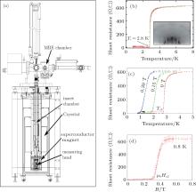 | Fig. 6. Micro-4PP installed in a cryostat containing superconductor magnet for applying magnetic field in in situ transport measurements on    |
Previously developed micro-4PP measurement apparatus were equipped with only reflection high electron energy diffraction (RHEED) for monitoring the sample growth by molecule beam epitaxy. Although RHEED is helpful in a certain extent, a real-space observation in nanometer or even atomic scale will be more convincing for evaluation of the sample quality. As STM is a powerful tool for studying atomic and electronic structures of sample surfaces, it is desirable to develop an apparatus that is capable of both STM observations and micro-4PP electrical transport measurement. A four-tip STM consisting of four independently driven tips can intrinsically meet the requirements, just as the apparatus developed in Shiraki et al.’ s pioneering work.[14] However, external high magnetic field is difficult to be applied in a four-tip STM in technique mostly due to its large space occupation for holding the four tips above sample surfaces.
Fortunately, the surrounding structures of an STM tip holder are very similar to those of a micro-4PP holder, which inspired Ge et al. to develop a micro-4PP apparatus that is compatible with commercial STM.[40] The key issue in the development is to invent a piezo-activated probe stage that works not only for STM tip holders but also for 4PP holders. Figure 7(a) is the schematic illustration of the developed probe stage, in which a piezo tube is firmly fixed on a piezo stage. Such a structure is basically the same as that of a Pan-type STM probe stage. The main modification in this design is that the piezo tube contains four electrodes that are necessary for 4PP electrical transport measurement. Accordingly, the 4PP holder has also a four-electrode rod that can be inserted into the piezo tube, as shown in Figs. 7(a) and 7(b). The piezo tube and the 4PP holder was made by following the design of earphone socket and plug, respectively. As STM needs only one electrode, the rod of STM tip holder is shorter, as shown in Fig. 7(d). Figures 7(c) and 7(e) show photograph of the 4PP and STM-tip holders, respectively.
The Micro-4PP used in Ge et al.’ s development is basically the same as that of Hasegawa et al.’ s, as shown in Fig. 7(f). As the metal-coated cantilevers of the micro-4PP tips are fragile, and thus may be easily broken due to mechanical pressure resulted from, e.g., large-range temperature variation, the 4PP made of four fine copper wires was also usually used, as shown in Figs. 7(g) and 7(h). The tip spacing of the Cu-wire 4PP is typically about 100 μ m, which is still quite small compared with the lateral size of sample specimen, i.e., 2 × 8 cm2.
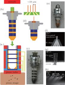 | Fig. 7. Development of 4PP that is compatible with STM.[40] (a) Schematic drawing of the deformed probe stage. (b), (c) Schematic drawing and photograph of the 4PP holder, respectively. (d), (e) Schematic drawing and photograph of the STM tip holder, respectively. (f) Photograph of Si-chip based micro-4PP, taken via optical microscope. (g), (h) Photograph of Cu-wire 4PP taken from different view angles via optical microscope. |
With the STM-compatible 4PP measurement system, Ge et al. measured the electrical transport properties of single-layer FeSe films grown on Nb-doped STO, and revealed that the superconductivity transition temperature is above 100 K.[8] The growth process of FeSe films was monitored by RHEED, as shown in Fig. 8(a). The crystalline quality was checked by STM in both large- and atomic-scale images, as shown in Figs. 8(b) and 8(c), respectively. Differential conductance (dI/dV) spectra were also obtained on the FeSe films at 77 K by means of STS, as shown in Fig. 8(d). Reliable superconductive energy gap of the single-layer FeSe/STO could not be observed yet due to the high noise level of the instrument, which still needs optimization for noise suppression.
The in situ 4PP transport measurement of the FeSe/STO was carried out after the exchange of 4PP and STM tip holders on the tip stage. Driven by the STM tip approach system with feed-back circuit, one of the 4PP tips will touch the sample surface first and gently. Then, the feed-back circuit was turned off for further tip approaching till all of the four tips touch the sample firmly. The electrical contacts between tips and sample were confirmed by measuring the two-electrode I– V curves between each tip and the sample, as shown in Fig. 10(a). The linearity of the I– V curves in the current range of ± 1 mA indicates a nearly Ohmic contact.
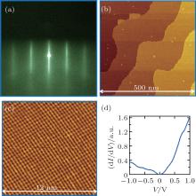 | Fig. 8. Synthesis of single-layer FeSe film grown on Nb-doped STO substrate.[8, 40] (a) RHEED pattern of FeSe/STO. (b), (c) STM images of FeSe/STO in large and atomic scale, respectively. (d) dI/dV curve taken on FeSe/STO at 77 K. |
Figure 9(b) shows the temperature dependence of zero-bias resistance extracted from a series of 4PP I– V curves, some of which are shown in the inset.[8] The resistance value drops from several mΩ to less than 1 μ Ω , which is the accuracy of the electrical measurement system, indicating that a superconductive transition occurs at ∼ 109 K. The critical current (Ic) can be extracted from the 4PP I– V curves, and its temperature dependence was fitted to the Ginzburg– Landau model[41]
 |
as shown in Fig. 9(c). The fitting result with Ic(0) = 3.8± 0.2 mA and Tc = 111± 4 K agrees well with the Ic and Tc values obtained directly from the I– V curves at fixed temperatures.
Due to the sample inhomogeneity and/or possible sample damages caused by tip-sample contacts, the R– T plot shown in Fig. 9(b) was completed by collecting I– V curves at different locations for different temperatures. Ge et al. have also performed the 4PP measurement on another sample with the tips fixed at one location, while temperature was varied, and obtained R– T data showing a Tc value of around 99 K, as shown in Figs. 10(a) and 10(b).
It is theoretically expected that a 2D superconductor should exhibit a gradual change in resistance during superconductive transition, i.e., the Berezinsky– Kosterlitz– Thouless (BKT) transition.[42] In the in situ 4PP electrical transport measurement, however, the transition is very sharp and shows no signature of the BKT transition, as shown in Fig. 10(b). This unexpected behavior is actually due to the high conductivity of the STO substrate that is necessary for the growth of high-quality single-layer FeSe films in practice. Figure 10(c) is a schematic illustration qualitatively explaining the sharp transition of the measured resistance. At high temperature (higher than Tc), the FeSe/STO is still a normal metal with a resistance on the order of 10 Ω , which is much larger than that of the Nb-dope STO substrate (several mΩ ). Therefore, the applied current flows mainly through the substrate, and thus the measured 4PP resistance reflects the electrical transport property of the STO substrate. At temperatures lower than Tc, in contrast, the current flows mainly through the superconductive FeSe/STO, resulting in the measured zero resistance. In other words, the higher-temperature parts of the measured 4PP resistance in Figs. 9(b) and 10(b) are not the normal-state resistance of the single-layer FeSe/STO, but that of the Nb-doped STO substrate.
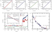 | Fig. 9. Results of in situ 4PP transport measurement on single-layer FeSe/STO.[8, 40] (a) Linear I– V curves recorded between each 4PP tip and the FeSe/STO sample, indicating nearly Ohmic contacts. (b) Temperature dependence of zero-bias resistance measured at different tip locations. Inset is some typical 4PP I– V curves recorded at around 110 K. (c) Temperature dependence of critical current. The solid curve is a fit to Eq. (6). |
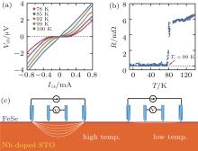 | Fig. 10. Results of in situ 4PP transport measurement on single-layer FeSe/STO.[8] (a) A series of I– V curves taken at a fixed tip location and different temperatures. (b) Temperature dependence of zero-bias resistance extracted from the I– V curves, showing a sharp transition at around 99 K. (c) Schematic illustration explaining the sharpness of the transition found in panel (b). |
Figure 11 shows the influence of external magnetic fields on the electrical transport properties of the single-layer FeSe/STO at varied temperatures. At 3 K, Ic decreases monotonically with increasing magnetic field, and remains non-zero up to 11 T, as shown in Fig. 11(a), indicating that the FeSe/STO has a large critical magnetic field. At around Tc, the temperature dependence of zero-bias resistance measured under magnetic field shows similar superconductive transition to that at zero field, and the only difference among them is that Tc decreases monotonically as the magnetic field increases, as shown in Fig. 11(b). Furthermore, 4PP measurement were carried out at fixed temperatures, while the magnetic field was swept, as shown in Fig. 11(c). At 100 K, zero resistance never occurs, even at zero field, in consistence with the R– T result shown in Fig. 10(b). The critical field, Hc, increases remarkably with decreasing temperature until 95 K, from which Hc was found to be greater than 10 T. Figure 11(d) shows values of the critical field obtained at different temperatures (from Figs. 11(b) and 11(c)), and a fit to an empirical equation[41]
 |
This fit gives a zero-temperature μ 0Hc = 116± 12 T and zero-field Tc = 99.3± 0.2 K. These results show well that the observed zero resistance detected by the in situ 4PP measurement is the signature of superconductivity, which could be destroyed by a sufficiently strong magnetic field. It should be noted that the value of Tc obtained in the fitting result is slightly smaller than that found in Fig. 9. It is possibly owing to sample quality.
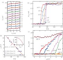 | Fig. 11. Influence of external magnetic field on the electrical transport properties of the FeSe/STO.[8] (a) A series of I– V curves taken under varied magnetic fields at 3 K. (b) Temperature dependence of measured 4PP resistance at various external magnetic field. (c) Magnetic-field dependence of measured 4PP resistance at various temperatures around Tc. (d) Relation between the critical values of magnetic field and temperature. Filled triangles and circles are experimental results deduced from panels (b) and (c), respectively. Error bars are defined by the difference of temperatures where the measured resistance reaches zero. The solid line is a fit to Eq. (7). |
The development of three in situ four-electrode transport measurement instruments has been introduced. Their successful applications to the studies of superconductive ultrathin films, which are usually very fragile to atmosphere, demonstrated well that the in situ transport measurement is very suitable and necessary for this research field. Not only zero resistance, the influence of external magnetic fields on the superconductivity of ultrathin films can be also observed in in situ transport measurements. Various critical parameters, such as Ic, Tc, and Hc, of superconductive ultrathin films can all be obtained.
| 1 |
|
| 2 |
|
| 3 |
|
| 4 |
|
| 5 |
|
| 6 |
|
| 7 |
|
| 8 |
|
| 9 |
|
| 10 |
|
| 11 |
|
| 12 |
|
| 13 |
|
| 14 |
|
| 15 |
|
| 16 |
|
| 17 |
|
| 18 |
|
| 19 |
|
| 20 |
|
| 21 |
|
| 22 |
|
| 23 |
|
| 24 |
|
| 25 |
|
| 26 |
|
| 27 |
|
| 28 |
|
| 29 |
|
| 30 |
|
| 31 |
|
| 32 |
|
| 33 |
|
| 34 |
|
| 35 |
|
| 36 |
|
| 37 |
|
| 38 |
|
| 39 |
|
| 40 |
|
| 41 |
|
| 42 |
|


