Liu Can-Huaa), b)  , Jia Jin-Feng
a), b)
, Jia Jin-Feng 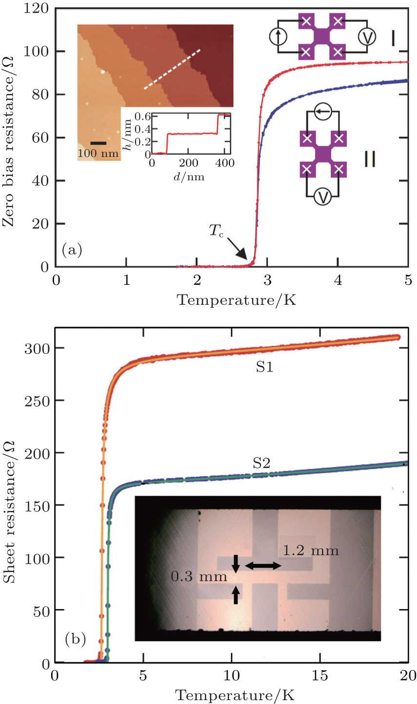
|
Liu Can-Hua
, Jia Jin-Feng |
| Transport experimental evidence for the superconductivity of the -In surface.[ 10 , 11 ] (a) Results of in situ four-terminal electrical transport measurement using the nanostencil-fabricated electrodes in Van der Pauw’s configuration. Inset is the typical STM image of the -In surface. Inset is the line profile along the dotted line, showing the atomic steps of the Si(111) substrate. (b) Results of in situ four-terminal electrical transport measurement using the nanostencil-fabricated electrodes in linear configuration. Inset is an optical microscope image of the patterned sample. |
| |