


Design of patterned sapphire substrates for GaN-based light-emitting diodes*
[Wang Hai-Yana) , Lin Zhi-Tinga) , Han Jing-Leia) , Zhong Li-Yia) , Li Guo-Qianga), b)  ]
]
]
|
|


†Corresponding author. E-mail: msgli@scut.edu.cn
*Project supported by the National Natural Science Fundation for Excellent Young Scholars of China (Grant No. 51422203), the National Natural Science Foundation of China (Grant No. 51372001), the Outstanding Youth Foundation of Guangdong Scientific Committee (Grant No. S2013050013882), and the Strategic Special Funds for LEDs of Guangdong Province, China (Grant Nos. 2011A081301010, 2011A081301012, 2012A080302002, and 2012A080302004).
A new method for patterned sapphire substrate (PSS) design is developed and proven to be reliable and cost-effective. As progress is made with LEDs’ luminous efficiency, the pattern units of PSS become more complicated, and the effect of complicated geometrical features is almost impossible to study systematically by experiments only. By employing our new method, the influence of pattern parameters can be systematically studied, and various novel patterns are designed and optimized within a reasonable time span, with great improvement in LEDs’ light extraction efficiency (LEE). Clearly, PSS pattern design with such a method deserves particular attention. We foresee that GaN-based LEDs on these newly designed PSSs will achieve more progress in the coming years.
Since the first high-brightness GaN-based blue light-emitting diode (LED) was achieved on flat c-plane sapphire substrate, LEDs have been widely used in diverse areas, [1– 3] such as displays, traffic signals, automobile headlamps, and lighting. The trend in LED development is heading to high-power and high-efficiency general lighting devices based on sapphire substrates. However, further development of such devices is hindered by two main obstacles. First, the crystalline defect density in GaN is high, resulting from the relatively large lattice mismatch between GaN and sapphire, [4– 6] and this impacts the internal quantum efficiency (IQE) of LEDs. Second, the light extraction efficiency (LEE) is low due to a severe total reflection effect between GaN and sapphire.[7, 8] To cope with these problems, significant progress has been made. On one hand, there are two main methods for improving IQE. The first is to employ special epitaxial technologies to reduce the crystalline defect density of epitaxial wafers.[9– 11] The second is to adopt advanced epitaxial structures to improve the carrier radiative recombination rate and avoid carrier leakage.[12– 14] On the other hand, the approaches to improving LEE are still under active research, with various proposed methods, including pattered sapphire substrate (PSS), [15, 16] Bragg reflection layers, [17] photonic crystal, [18] surfaces roughing, [19] flip-chip packing.[20] However, some of these approaches have corresponding drawbacks, making them very challenging in real applications. For example, Bragg reflection layers and photonic crystal bring foreign material layers into the LED epitaxial structures, posing extra epitaxial difficulties and thus deteriorates the crystalline quality of GaN. Among these methods, PSS shows great promise because it is capable of improving LEE and crystalline quality simultaneously. It has attracted intensive interest and has already become a standard procedure for GaN-based LED manufacture.
This review focuses on PSS technology that is employed in the fabrication of LEDs. The working mechanisms, advantages, and development of PSS are systematically covered. Moreover, a new method for PSS design through computer simulations, together with novel patterns, is also discussed in detail.
PSS is a new type of sapphire substrate with dense patterns periodically arranged on the substrate surface via semiconductor etching. To date, it has proven advantageous for improving the efficiency of LEDs, owing to its superior properties.
On one hand, PSS enables one-step epitaxial growth technology to achieve the lateral growth of GaN, which is beneficial to overcome the disadvantages of the two-step epitaxial process.[16] As mentioned above, the large lattice mismatch between sapphire and GaN of ∼ 14%[4] leads to a high defect density of up to 109 cm− 2∼ 1010 cm− 2 in GaN films grown on conventional flat sapphire substrates.[4] Such massive crystal defects serve as non-radiative recombination centers and therefore decrease carrier lifetime and radiative recombination efficiency, [21, 22] which reduces the IQE of LEDs. In this regard, employing PSS can promote the epitaxial lateral overgrowth (ELOG) mode and consequently reduce the defect density of GaN.[16] Figure 1 illustrates the growth mechanism of GaN on PSS, where the twisty black lines represent dislocations. In the initial stage of GaN growth on PSS, Fig. 1(b), the GaN grains nucleating on pattern windows grow fast, perpendicular to the substrate, accompanied by many dislocations extending vertically.[23] When GaN grows higher than the patterns, the slanted side facets promote the lateral growth of GaN, and therefore cause some dislocation bending, Fig 1(c).[24] Eventually, as the thickness of as-grown GaN films increases, the dislocations propagating from the side facets of PSS close together, Fig. 1(d). In this way, defects in the MQWs layer are effectively reduced.
 | Fig. 1. The evolution of GaN epitaxial layer and dislocations on PSS, (a) before growth, (b) during lateral growth, (c) during coalescence, and (d) after coalescence. |
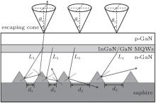
On the other hand, pattern units on PSS serve as light scattering elements that improve the LEE of LEDs. Because of the great difference in refractive index between GaN (nGaN = 2.45) and sapphire nsapphire = 1.78), the critical angle for light escaping from the device into the air is only 24.6° .[25] Hence, a large proportion of the rays are confined in the LED chip, which seriously limits the LEE of LEDs.[26] To solve this problem, PSS is adopted to modify the light path and ultimately to break the total reflection effect. As illustrated in Fig. 2, rays are repeatedly scattered by pattern units on PSS, i.e., L1, L2, L3, and L4. Once the ray enters into the escaping cones, it can be emitted into the air. As a result, the LEE of LEDs is greatly enhanced.
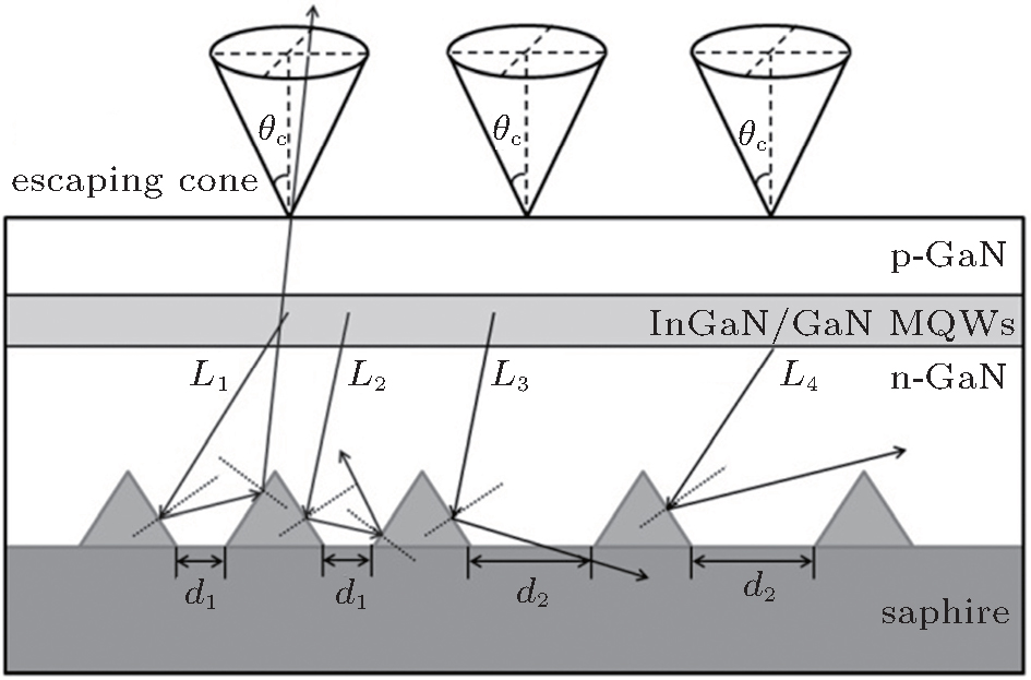 | Fig. 2. The light path in PSS-LED. |
To sum up, PSS can not only raise the ELOG mode, effectively improving the crystalline quality of GaN, but also act as the light scattering elements to increase the proportion of rays emitted, which helps to enhance the LEE of LEDs.
As PSS technology developed, various patterns including groove, [24, 27] hexagonal frustum, [28] trigonal frustum, [29] hemisphere, [30– 32] and cone[33, 34] were proposed.
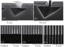
In the early stage of development, the main limitation of PSS fabrication was the lack of advanced etching technologies, so grooved patterns with simple geometrical features were first put forward. According to the shapes of pattern units, grooved PSS can be divided into three main types — straight groove, [35] slanted groove, [27] and V-shaped groove PSSs, [27] as illustrated in Fig. 3.
 | Fig. 3. SEM images of the grooved PSS: (a) straight, [35] (b) slanted, [27] and (c) V-shaped grooves.[27] |
Jiang et al.[27] reported the growth mechanism of GaN grown on V-shaped groove PSSs. During the initial low-temperature growth, GaN nucleation centers are distributed uniformly on the platform and window areas of patterns, followed by a redistribution into strip-shaped areas during annealing. Subsequently, strips of GaN are grown at high temperature in ELOG mode and finally coalesce into a film with air gaps left beneath it, as shown in Fig. 4. Apart from the shape of pattern units, depth is also an important factor for grooved PSS. Pan et al.[24] studied the influence of groove depth on the luminous efficiency of LEDs, as shown in Table 1. It was revealed that as the depth increases, the photoluminescence (PL) intensity of LEDs increases accordingly. When the depth is 0.9 μ m, the PL intensity of 

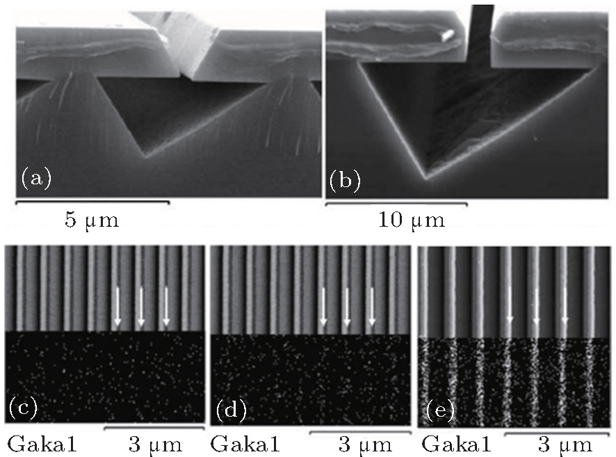 | Fig. 4. SEM images of the air gaps of V-shaped-groove PSSs with different pattern periods of (a) 6 μ m and (b) 18 μ m; GaN nucleation distribution of V-shaped-groove PSSs in different stages: (c) low-temperature 30-nm-thick GaN nucleation; (d) annealing; (e) high-temperature 0.5-μ m-thick GaN layer.[27] |
| Table 1. The effect of grooved PSSs on the PL intensity and etch pit density.[24] |
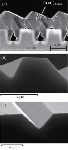
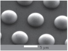
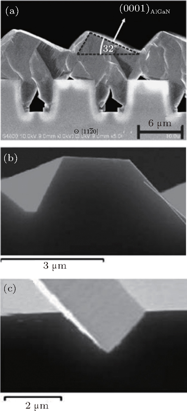
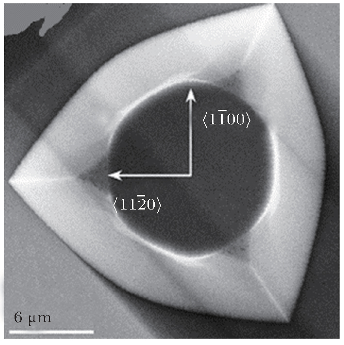
In order to solve the problem of luminescence inhomogeneity and further improve the performance of LEDs, pyramid-patterned PSS was developed. This type of PSS has pattern units densely distributed in two dimensions that enable GaN to grow homogeneously on the substrate. Meanwhile, compared to grooved patterns, pyramid patterns provide more slanted planes for light scattering, and therefore enhance the LEE of LEDs. Among the series of pyramid patterns, the hexagonal frustum, triangular frustum, and triangular pyramid are easily fabricated by wet etching technology, due to the hexagonal crystalline structure of sapphire. Shown in Fig. 5 are hexagonal frustums 100 nm to 4.5 μ m in width, 100 nm to 2 μ m in height, and 10 nm to 3 μ m in distance.[28] Unlike a groove, one hexagonal frustum has six side facets, which can scatter incident light from all directions. If the pattern units are densely arranged with a proper density, the scattering area can be larger than that of grooved PSS. Consequently, the light scattering effect is enhanced, and the LEE of LEDs is greatly improved. Figure 6 illustrates the typical triangular frustums fabricated by wet etching, 1 μ m∼ 3 μ m in width, 0.2 μ m∼ 1.5 μ m in height, with centers separated by 1 μ m∼ 3 μ m. Depending on the etching time, triangular frustums can be transformed into triangular pyramids.[34]
 | Fig. 5. SEM images of hexagonal frustums:[28] (a) top view; (b) cross section view. |
Figure 7 indicates that as the etching time increases, C-PSS and D-PSS are transformed into triangular-pyramid-patterned PSSs while A-PSS and B-PSS remain as triangular-frustum-patterned PSSs. Table 2 shows the effect of distance on the GaN crystalline quality and the luminous efficiency of LEDs. With the distance decreasing, both the (0002) and 
 | Fig. 6. SEM image of triangular frustum.[29] |
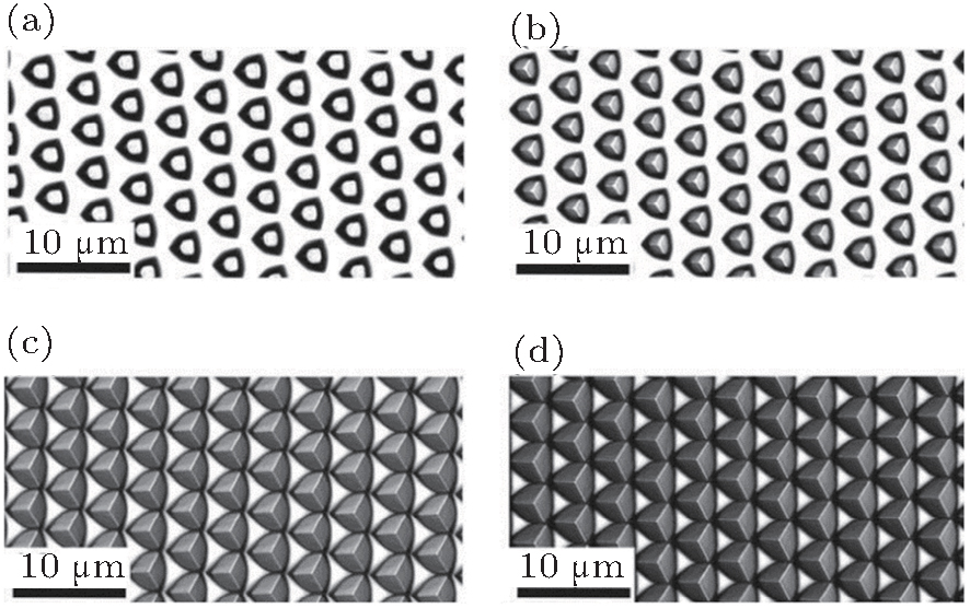 | Fig. 7. The evolution of pattern units with wet etching time: (a) A-PSS, (b) B-PSS, (c) C-PSS, and (d) D-PSS.[34] |
| Table 2. The effect of the distance on the crystalline quality of GaN and the luminous efficiency of LEDs.[34] |
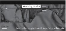
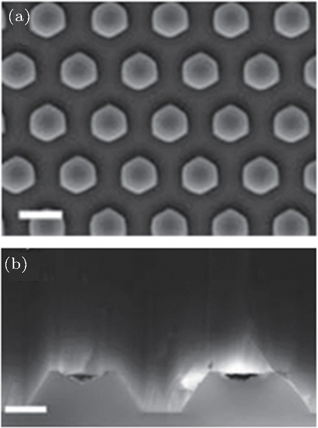
Apart from pyramid-patterned PSS, the patterns on hemisphere-patterned PSS are also distributed two-dimensionally, with approximately hemispherical surfaces, as shown in Fig. 8. Jaehee, [36] Lee et al., [37] Jeong et al.[38] reported that the ELOG effect can be enhanced by close-arranged hemispheres, which results in great improvement in crystal quality. Shin et al.[39] utilized ICP etching to fabricate hemispherical patterns with 2.5-μ m spacing, and 1.5-μ m height on sapphire substrates. The GaN films grown on these PSSs by MOCVD exhibit better crystal quality, with the dislocation density reduced to 107 cm− 2. During the initial growth, GaN nucleation centers grow primarily on the platform areas between hemispheres, and the top areas of hemispheres.
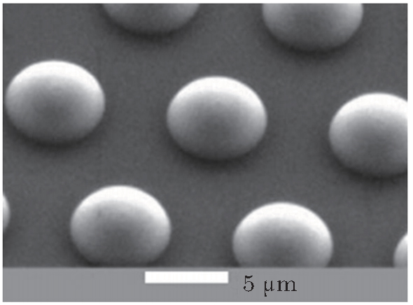 | Fig. 8. SEM image of hemisphere-patterned PSS.[38] |
When GaN films grow thicker than the height of the hemispheres, the GaN nucleation centers on the top areas serve as the steps to absorb Ga and N atoms, promoting the ELOG of GaN. Figure 9 exhibits the stacking faults formed by ELOG on the top areas of hemispheres. Such stacking faults restrain the extension of threading dislocations into the active region, which leads to higher quality multiple quantum wells.
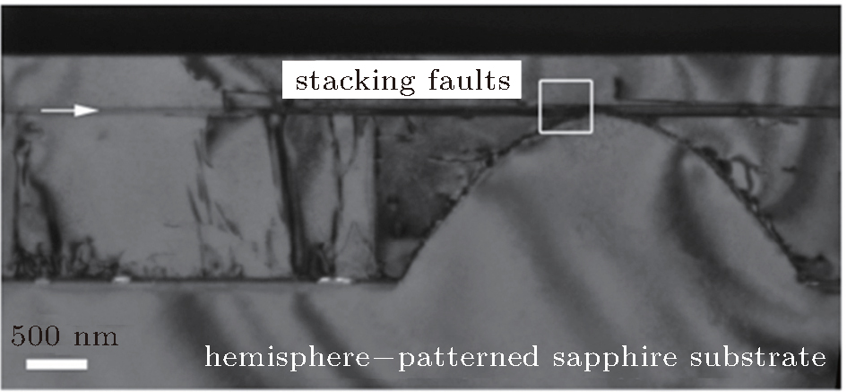 | Fig. 9. TEM image of stacking faults on the top of hemisphere (indicated by white arrow).[30] |
It is obvious that hemisphere-patterned PSS can greatly improve the crystal quality of GaN and thereby enhance the IQE of LEDs. However, to improve the LEE of LEDs, PSS still needs to be further optimized.
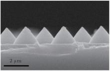
Cone-patterned PSS, as shown in Fig. 10, is developed from hemisphere-patterned PSS. The slanted facets introduced by cone patterns are beneficial to the light scattering of incident rays, and thus improve the LEE. It is reported that different parameters of cone patterns, such as height, distance, and width, have significant effects on the crystal quality of as-grown GaN films and the luminous efficiency of LEDs. Cheng et al.[34] used wet etching technology to fabricate cone-patterned PSSs of different heights. Subsequent crystal growth reveals that the density of dislocations in GaN decrease with decreasing height, indicating that threading dislocation density is related to the area of GaN lateral growth. When undergoing lateral growth, threading dislocations in GaN tend to bend and stop growing toward the MQWs layer. As the pattern height is low, the area of lateral growth increases correspondingly. As a result, dislocations are limited in the n-GaN layer, contributing to better quality MQWs. In addition to the height, the influence of the patterns period length on LED luminous efficiency has also been investigated. Lee et al.[40] fabricated LED devices on cone-patterned PSSs 3 μ m in width, 1.5 μ m in height, with 1 μ m∼ 3 μ m spacing. The light output power for cone-patterned PSS LEDs increase gradually with decreasing distance between cones. Compared to the output power of an LED on conventional flat sapphire substrate, the LED on PSS with the closest spacing is enhanced by 1.9 mW under an injection current of 20 mA.
As a critical part of PSS technology, various patterns play significant roles in the improvement of LED luminous efficiency. To explore the optimal PSS, researchers have to routinely conduct a large number of experiments to evaluate the effects of different parameters. The entire LED device fabrication process and characterization must be run through, which is time-consuming and not very cost-effective. Further, this lengthy procedure with many steps greatly enlarges the possibility of errors and contributes inaccuracy and uncertainty to the results. To overcome these drawbacks, a new methodology for PSS design by computer simulations is hence introduced by our group.[42] An optical analysis software TracePro is utilized to run the simulations. By this means, researchers can deploy various patterns and optimize them within a reasonable time span, which is advantageous to reduce the time for PSS design, and greatly improve research efficiency. Furthermore, subsequent crystal growth and characterizations of LED wafers have verified the effectiveness and reliability of this new methodology.
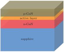
The simulation procedure includes four steps, that is, building an LED chip model with PSS layer, defining a Lambertian light source, tracing rays, and collecting data. Figure 11 exhibits the LED chip model built in the first step. Diverse patterns with given parameters are subsequently built on the surface of sapphire substrate. Refractive index and thickness for each layer are shown in Table 3. The mole fraction of indium in InGaN/GaN multiple quantum wells (MQWs), which is represented by the “ active layer” here, is set as 15%. All the parameters are set according to real LED devices to ensure the reliability of the model. The second step is to set up the top and bottom planes of the “ active layer” as Lambertian light sources. The output power and total number of rays can be set as any given values, respectively. Then light emitting conditions of the LED chip are simulated via the ray-tracing function integrated in TracePro. To collect the emergent rays from the LED chip, six virtual targets with no material properties are built close to corresponding facets. After the model is complete with all geometry and parameters in position, TracePro will present the luminous flux from each facet according to its mathematical function.
 | Fig. 11. Schematic diagram of the LED chip model’ s structure. |
| Table 3. Refractive index and thickness of each layer of the LED chip model. |
Through our work, various PSSs such as grooved PSS, hemisphere-patterned PSS, and cone-patterned PSS have been systematically optimized.[42– 44] Furthermore, based on the optimization results, two novel PSSs, the so-called spherical cap-patterned PSS and dome-patterned PSS, have been proposed for high-efficiency GaN-based LEDs.[43, 44]
Spherical cap-patterned PSS (SCPSS) is derived from hemisphere-patterned PSS (HPSS) by changing the height of its hemispherical units. As shown in Fig. 12, three parameters of spherical cap pattern have been optimized including intercepted ratio, edge spacing, and radius of pattern.
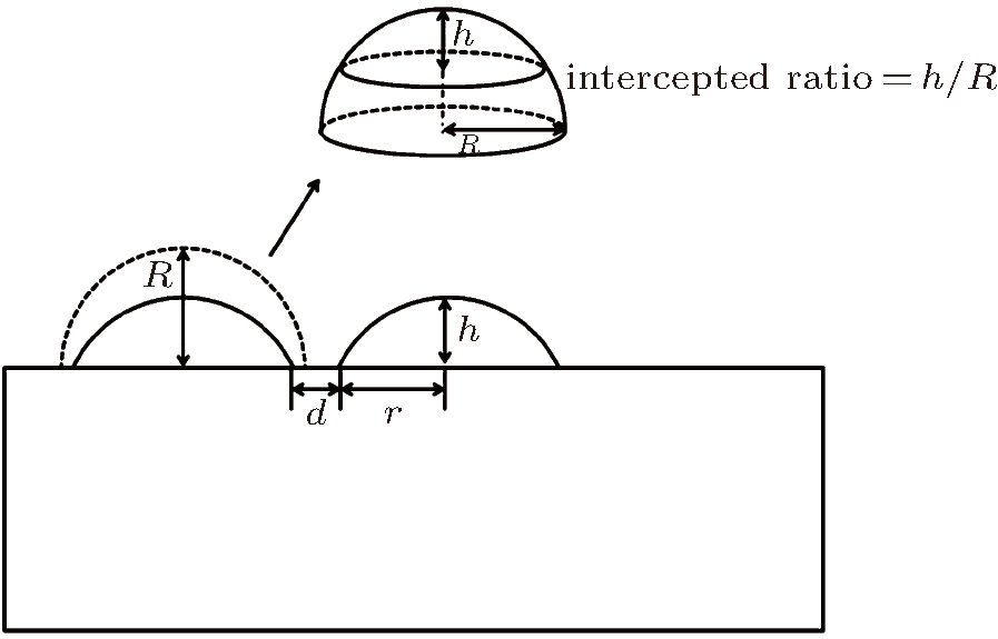 | Fig. 12. Schematic diagram of the definition of parameters for spherical cap-patterned PSS. |
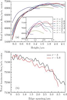
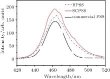
Figure 13(a) shows total luminous fluxes of SCPSS LEDs with various radii as a function of the intercepted ratio. In general, total luminous fluxes rise at first with an increase of intercepted height, with maximum value reached at the intercepted ratio of 60%∼ 85%, and then drop slowly. As for edge spacing, figure 13(b) suggests that total luminous fluxes decrease constantly with the decrease of edge spacing. It is demonstrated that an LED grown on the optimal SCPSS, 3.4 μ m in radius, 2.78 μ m in height, with 1.7 μ m edge spacing, achieves the maximum LEE. To verify the accuracy of computer simulations, subsequent crystal growth and characterizations of LED wafers on such PSSs have been carried out. Shown in Fig. 14 are the EL spectra from LED chips grown on HPSS, SCPSS, and a commercial PSS. It reveals that the LEE of the LED grown on the optimal SCPSS is enhanced by more than 10% compared with that on HPSS, which agrees well with the simulation results, proving the legitimacy and reliability of this new methodology.
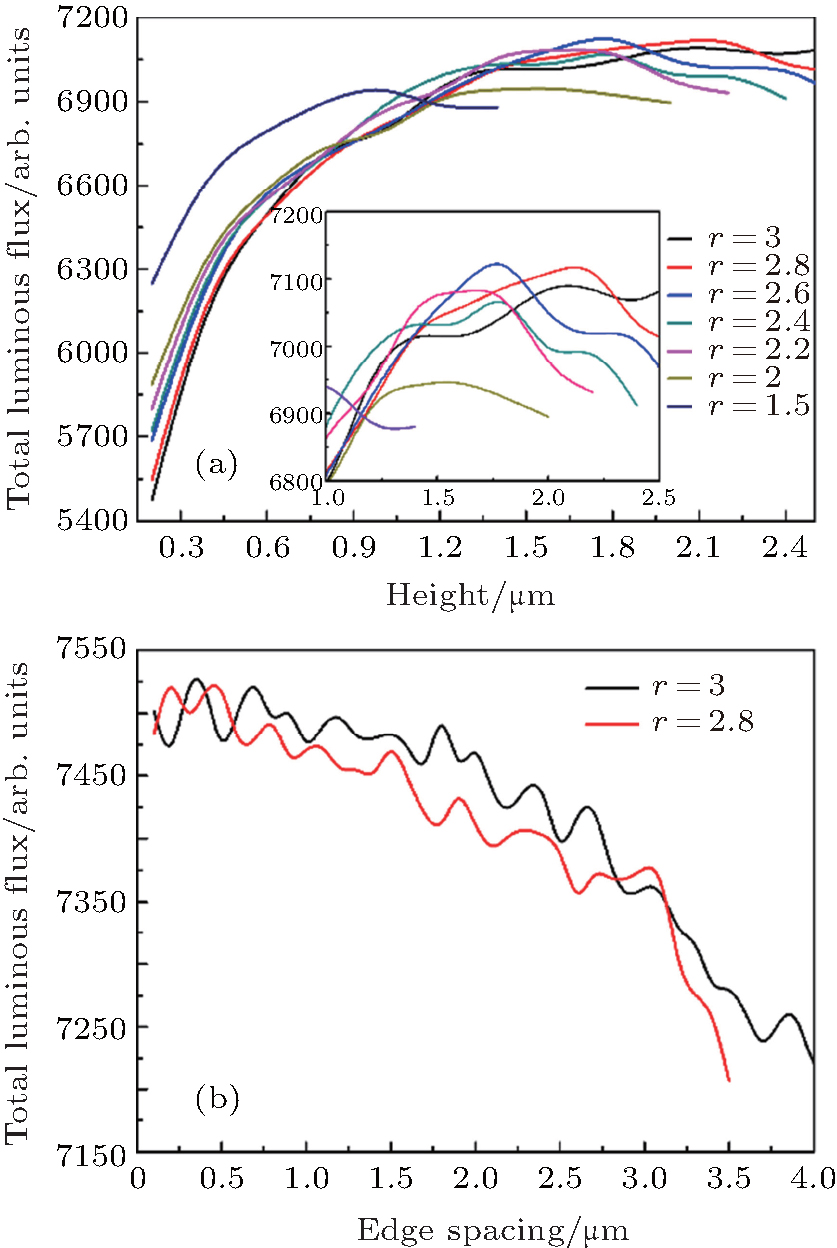 | Fig. 13. Total luminous flux of SCPSS LEDs as functions of (a) height and (b) edge spacing. |
 | Fig. 14. EL spectra from LED chips grown on HPSS, SCPSS, and a commercial PSS. The SCPSS is of optimal dimensions: 3.4 μ m in radius, 2.78 μ m in height with 1.7 μ m edge spacing, and the HPSS is 3.45 μ m in radius with 1.6 μ m in edge spacing which is the SCPSS intercepted with an interception ratio of 0.8. |
In addition to hemisphere-patterned PSS, our group[42] has also performed detailed investigations on the effects of different cone-patterned PSSs (CPSSs). It is pointed out that when the straight generatrix of a cone pattern becomes curved, the transmitting path of photons in LED chips changes immediately, which greatly affects the LED’ s luminous efficiency. In this regard, a novel type of PSS is put forward thereafter, the so-called dome-patterned PSS (DPSS).[44]
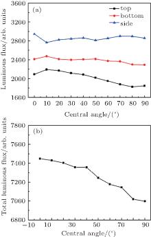
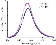
Figure 15 exhibits the cross-sectional morphology of DPSS. According to simulation results shown in Fig. 16, the DPSS LED (D-LED) with 10° in the generatrix’ s central angle presents the highest top and bottom luminous flux, and its total flux remains relatively high. Furthermore, EL characterizations of LED chips, shown in Fig. 17, reveal that the luminous intensity from an optimal DPSS LED is enhanced by 19% compared to that of a CPSS LED (C-LED) with the same dimensions. These results straightforwardly confirm the effectiveness of optimal DPSS for improving LED luminous efficiency.
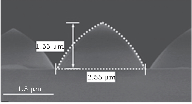 | Fig. 15. Cross-sectional SEM image of DPSS. |
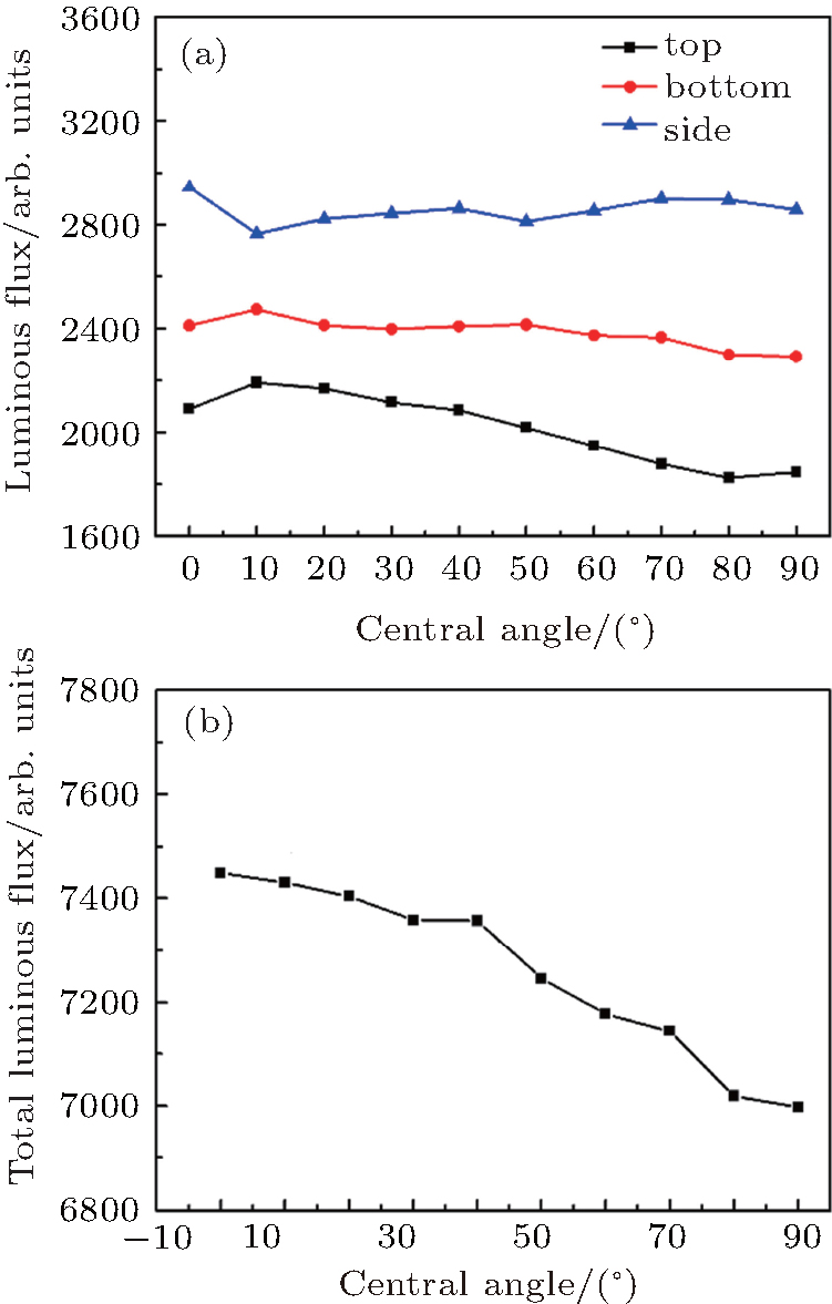 | Fig. 16. (a) Luminous fluxes from each facet and (b) total luminous flux of DPSS LED. |
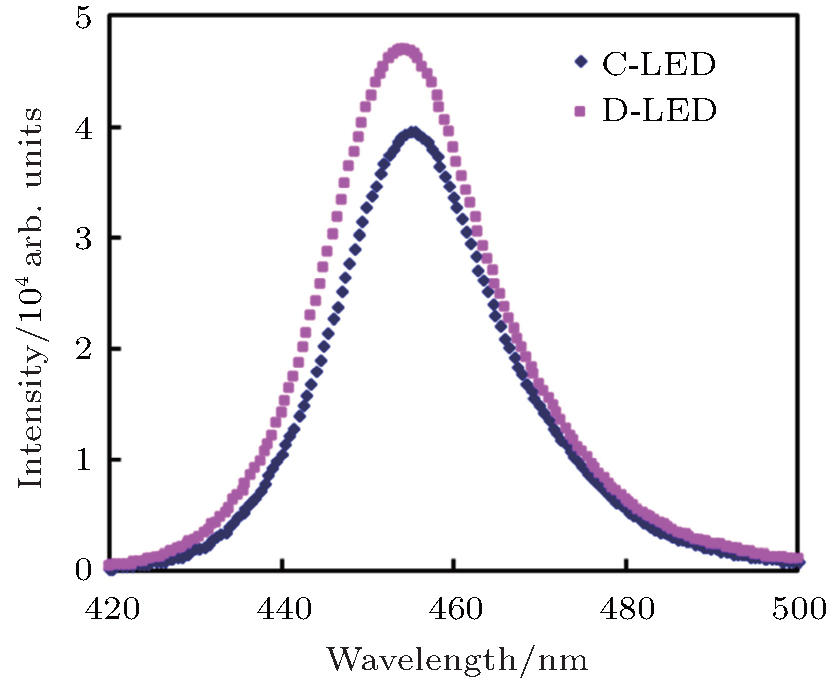 | Fig. 17. EL spectra of LEDs on DPSS and CPSS. |
In this review, we have discussed one of the most exciting and promising research directions in the field of LEDs. PSS is of paramount importance for LEDs because it greatly improves the crystal quality of GaN and the LEE of LEDs. PSS pattern units have become more and more complicated. The first and simplest pattern unit was a groove, and its one-dimensional geometrical feature limited further improvement of LEE. Afterward, various two-dimensional geometrical pattern units, such as hexagonal frustum, trigonal frustum, triangular pyramid, hemisphere, and cone, were put forward. It has been verified that such complicated patterns are very effective in improving LEDs’ luminous efficiency. However, the design of such novel PSSs faces a challenge, in that the effects of complicated geometrical features are almost impossible to systematically study by experiments only. Thus, a new methodology for PSS design by computer simulations is proposed herein, which is proven to be reliable and cost-effective. By employing this method, the influence of pattern parameters can be systematically studied. Therefore, various novel patterns can be designed and optimized within a reasonable time span. The field of pattern design with such methods still needs particular attention, since novel patterns designed by this method have potential for further improvement of the LEE of LEDs in the near future.
| 1 |
|
| 2 |
|
| 3 |
|
| 4 |
|
| 5 |
|
| 6 |
|
| 7 |
|
| 8 |
|
| 9 |
|
| 10 |
|
| 11 |
|
| 12 |
|
| 13 |
|
| 14 |
|
| 15 |
|
| 16 |
|
| 17 |
|
| 18 |
|
| 19 |
|
| 20 |
|
| 21 |
|
| 22 |
|
| 23 |
|
| 24 |
|
| 25 |
|
| 26 |
|
| 27 |
|
| 28 |
|
| 29 |
|
| 30 |
|
| 31 |
|
| 32 |
|
| 33 |
|
| 34 |
|
| 35 |
|
| 36 |
|
| 37 |
|
| 38 |
|
| 39 |
|
| 40 |
|
| 41 |
|
| 42 |
|
| 43 |
|
| 44 |
|