Design of patterned sapphire substrates for GaN-based light-emitting diodes
Wang Hai-Yana) , Lin Zhi-Tinga) , Han Jing-Leia) , Zhong Li-Yia) , Li Guo-Qianga), b) 
Design of patterned sapphire substrates for GaN-based light-emitting diodes |
|
Wang Hai-Yan
|
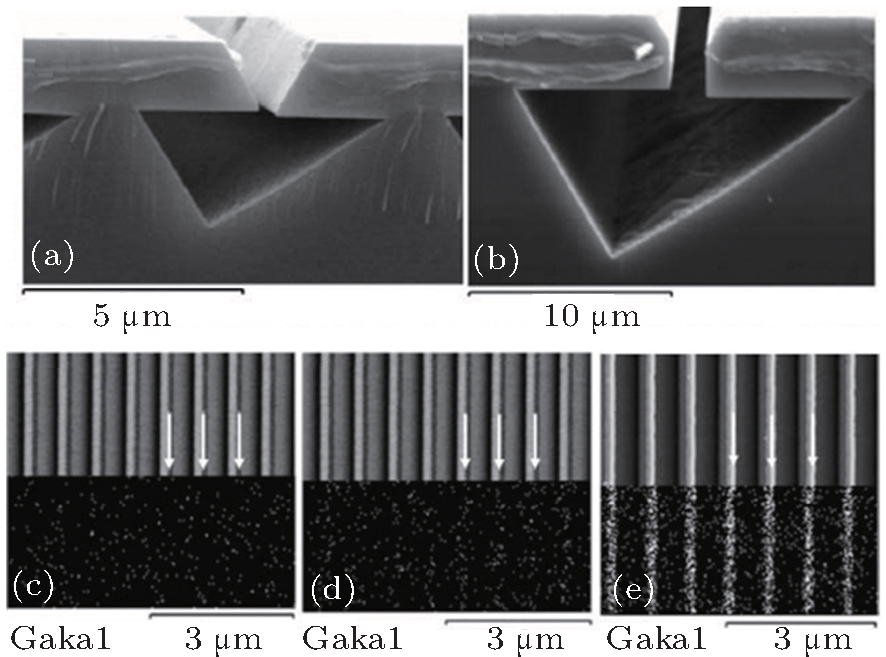
| SEM images of the air gaps of V-shaped-groove PSSs with different pattern periods of (a) 6 μm and (b) 18 μm; GaN nucleation distribution of V-shaped-groove PSSs in different stages: (c) low-temperature 30-nm-thick GaN nucleation; (d) annealing; (e) high-temperature 0.5-μm-thick GaN layer.[ 27 ] |
| |