† Corresponding author. E-mail:
Project supported by the Central University Basic Scientific Research Business Expenses Special Funds under the project name of Research on Applied Physics under Low Radiation Background (Grant No. 2018NTST07) and the National Natural Science Foundation Joint Fund Key Project, China (Grant No. U1865206).
Herein we report a prototypical electronic substrate specifically designed to serve the weakly interacting massive particles (WIMPs) detectors at the China Dark Matter Experiment (CDEX). Because the bulky high-purity germanium (HPGe) detectors operate under liquid-nitrogen temperatures and ultralow radiation backgrounds, the desired electronic substrates must maintain high adhesivity across different layers in such cold environment and be free from any radioactive nuclides. To conquer these challenges, for the first time, we employed polytetrafluoroethylene ((C2F4)n) foil as the base substrate, in conjunction with ion implantation and deposition techniques using an independently developed device at Beijing Normal University for surface modification prior to electroplating. The remarkable peeling strengths of 0.88±0.06 N/mm for as-prepared sample and 0.75±0.05 N/mm for that after 2.5-days of soaking inside the liquid nitrogen were observed, while the regular standards commonly require 0.4 N/mm ∼ 0.6 N/mm for electronic substrates.
Weakly interacting massive particles (WIMPs),[1–4] more commonly known as the candidates of dark matter, have been under extensive search collecting tremendous efforts worldwide.[5–14] Some notable efforts include CDMSlite[6] and LUX[7] from USA, CRESST-II[8] collectively from Great Britain, Italy, and Germany, as well as Pandax-II[12] and CDEX-10[13] from China. In their quests of search for WIMPs, various extreme measures have been undertaken to suppress radiation background that can potentially contribute to spurious counting of detectors. For instance, the experimental facilities are either positioned deeply underground[7–10] or inside a tunnel,[12–14] wherein the thick overlaying terrestrial layers serve to shield cosmic radiations, e.g., muon. Moreover, because the thermal noise from high-purity germanium (HPGe) detectors is also a considerable source of errors, the detector units are often cooled down to 77 K through immersing into liquid nitrogen (LN2).[13] Such a low temperature put some key components in the detector units to the serious test. In particular, the normal functioning of the electronic substrate which is responsible for transportation of the weak signals from the detector head to the succeeding amplifying electronics is critical. However, it is found that the regular commercial products, where different layers are glued together through common polymeric adhesive agents, can readily fail through delamination mechanism under this extreme environment. Hence, a cold-resistant high-adhesive electronic substrate is urgently needed to facilitate the ground-breaking study at CDEX. Furthermore, the desired product must also be free from any radioactive nuclides in order to be compatible with the ultralow radiation background and allow massive fabrication because the HPGe detectors are on the large scale of several tens of kilograms.
There are two different routes to enhance adhesivity for electronic substrate in the literature. One of them focuses on improving the polymeric glue through either changing their conformation or developing better substitutes with advanced properties. Though a remarkable peel strength up to several N/mm (e.g., RO3000® series from Rogers Corporation) has been achieved by following this strategy, a longstanding problem persists: due to different thermal expansion coefficients of the adhesives and the substrate layers, there can be appreciable residual stress on their interfaces accompanying significant temperature jump, which evidently increases the probability of failure at cryogenic conditions. In addition, the ceramic components and glass fibers from RO3000® series can also contaminate the ultralow-radiation environment. Therefore, this route is not considered here. Instead, we resort to the other route, namely surficial modification specifically based on ion beam implantation and deposition techniques.[15–21] To be more precise, the metal vapor vacuum arc (MEVVA) and filtered cathodic vacuum arc (FCVA)[16] are employed to develop the glue-free electronic substrates that can endure liquid-nitrogen temperatures. The FCVA technique, in comparison to magnet-controlled sputtering, yields ions with higher energies which in turn can effectively promote the ion deposition onto the substrate surface. Its combination with MEVVA can further enable interpenetration of atoms across the interfacial boundary thereby enhancing their bonding strengths. Although these techniques are not new,[22–24] their applications to fabricate electronic substrates that can serve WIMPs detectors are unprecedented.
In this pilot study, we started from the polytetrafluoroethylene (PTFE) as the base substrate because of its remarkably low radioactivity, which has motivated its widespread employment in rare-event experiments.[25–27] In order to improve the bonding between the dielectric and conduction layers, a combination of MEVVA and FCVA techniques using Ni+ and Cu2+ ion beams were applied to modify surface properties of the PTFE before electroplating. The intermediate and final products were characterized using scanning electron microscope (SEM) for surficial morphology, broadband dielectric impedance spectrometer for conductivity, and 90° peel strength tester for adhesivity.
The commercially available PTFE foil with thickness of 50 μm was employed as the base substrate, which was first cleaned using an ultrasonicator filled with alcohol and acetone, and then dried inside an oven set to 60 °C before use. An FCVA and MEVVA platform independently built at the Beijing Normal University was used for ion implantation and deposition. Throughout the operation, the vacuum level of the chamber was maintained lower than 3 mPa, the ion flux for MEVVA was around the order of 1016 ion/cm2, and the arc current and filtering magnetic fields for FCVA were approximately 90 A and 2 A, respectively. The cathodic materials were high-purity Ni for MEVVA, and Ni and Cu for FCVA. The designed sequential steps[28] for material processing are listed below:
The mechanism of improving the adhesivity between PTFE layer and the copper laminate layer can be qualitatively understood in the following manner. The Step 1 serves to modify the surface morphology of PTFE leading to increased surface energy and enlarged surface area owing to rough textures (see Subsection
Even though the PTFE processed after Step 1 is already applicable for deposition of Ni/Cu cohesion layers and subsequent electroplating, the so-fabricated electronic substrates were found to lack sufficient peel strength. Therefore, we designed a second round of ion implantation, i.e., Steps 2 and 3, where the Ni transition layer is expected to further enhance intermixing between Ni and PTFE atoms across their interface thereby increasing the interfacial bonding strengths. To illustrate this point, we carried out Monte Carlo simulations as demonstrated in Fig.
The SEM characterization on surface morphology of PTFE processed after Step 1 using 9-keV ions is shown in Fig.
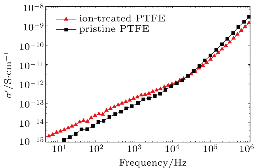
In the PTFE-based electronic substrate, the PTFE serves as the dielectric layer while the conduction layer on its top can be selectively etched out to make desired electric circuits. Therefore, it is essential for PTFE to remain insulating even after metallic ion implantation. To confirm this requirement, we characterized the conductivity of ion-treated PTFE using a broadband dielectric impedance spectrometer. The measurement results along with that from a pristine sample for comparisons are shown in Fig.
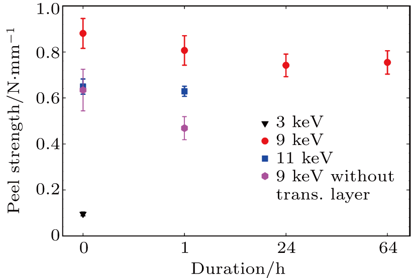
The aim of this work is to develop cold-resistant high-adhesive electronic substrates for WIMPs detectors at CDEX. To test adhesivity and its dependence on cryogenic temperatures, we immersed the final products in LN2 for a series of durations, after which the samples were put through 90° peel strength tester. Each tested stripe was carefully cut from the fabricated samples to ensure uniform width around 5 mm. Then the strip was peeled open on one end so that dielectric layer and conduction layer were separated. Next, we glued the whole dielectric layer horizontally onto the platform of the tester, and clamped the conduction layer from the peeled end using the mechanical claw, which is equipped with electronic readout on the pulling force. As the tester moves the mechanical claw, the peeling continues and the readout reflects the peel strength when the peeled layer and glued layer form 90°. This readout was later normalized by the stripe width. Note that all the tests were performed at the ambient temperature. Hence the results reflect potential degradation of bonding strength between PTFE and the copper laminate due to liquid-nitrogen temperatures. For each data point, at least three measurements were undertaken to estimate the confidence level. The results are depicted in Fig.
It is clear to see that the 9-keV sample (red disk) characterizes the highest peel strength among all as-prepared samples (0 h duration). In particular, the peel strength of the 3-keV sample (black triangle) is as low as 0.10 N/mm, which is clearly due to insufficient penetration strength of the comparably low-energy ions. Yet the peel strength of the 11-keV sample (blue square) is only around 0.65 N/mm, which can be attributable to carbonation. It appears that the ion energy around 9 keV is approximately an optimum choice. Moreover, the sample processed under 9 keV but without a transition layer (pink hexagonal) also shows much inferior adhesivity, ∼ 0.63 N/mm, which proves the necessity of a second round of ion implantation, namely Steps 2 and 3 in our protocol. The cold resistance of the 9-keV sample is also remarkable. The drop in peel strength after soaking inside the LN2 is very small, which is arguably within the experimental uncertainty. Even after around 2.5 days of immersion, the measured peel strength is found to only decay from 0.88±0.06 N/mm to 0.75±0.05 N/mm. To the best of our knowledge, this adhesivity is well beyond the requirement of 0.4 N/mm–0.6 N/mm for electronic substrates.
In summary, a prototypical sample that can be potentially employed as the electronic substrate for WIMPs detectors at CDEX was fabricated through ion implantation and deposition techniques for the first time. To reduce the radiation background from the raw materials, the PTFE was used as the base substrate. In the future, the high-purity oxygen-free copper, which is the most common structural material for HPGe detectors, will be employed for electroplating. The key findings are listed below.
(i) The electrical conductivity of the ion implanted PTFE show trivial changes in comparison to the pristine counterpart, which satisfies the requirement of the dielectric layer.
(ii) The ion-treated PTFE manifests considerably rough interface morphology, which is strongly dependent on the applied ion energy and is found to largely affect the adhesivity of the final products.
(iii) The peel strength of the as-prepared sample is as large as 0.88±0.06 N/mm and maintains the level of 0.75±0.05 N/mm after 2.5 days of soaking inside the liquid nitrogen.
The present study amounts to the first attempt to develop an ideal candidate of the electronic substrate to be used for WIMPs detectors at CDEX. The ion implanted and deposited PTFE shows tremendous promise for such an application. Furthermore, the roll-to-roll machine developed at the Beijing Normal University allows massive production of such substrates with bulk size. Admittedly, there are much room for further improvements and testing. The choices of ion energy and flux as well as transition layer thickness were based on prior experience on processing other substrates and hence warrant optimization in the future. In addition, a series of candidate substrate, such as polynaphthylene dimethyl acid glycol ester (PEN), will be considered. Furthermore, other critical parameters, such as thermal conductivity and thermal expansion coefficient, will also be tested.
| [1] | |
| [2] | |
| [3] | |
| [4] | |
| [5] | |
| [6] | |
| [7] | |
| [8] | |
| [9] | |
| [10] | |
| [11] | |
| [12] | |
| [13] | |
| [14] | |
| [15] | |
| [16] | |
| [17] | |
| [18] | |
| [19] | |
| [20] | |
| [21] | |
| [22] | |
| [23] | |
| [24] | |
| [25] | |
| [26] | |
| [27] | |
| [28] | |
| [29] |


