Defect engineering on the electronic and transport properties of one-dimensional armchair phosphorene nanoribbons
Xu Huakai, Ouyang Gang
Key Laboratory of Low-Dimensional Quantum Structures and Quantum Control of Ministry of Education, Key Laboratory for Matter Microstructure and Function of Hunan Province, Synergetic Innovation Center for Quantum Effects and Applications (SICQEA), Hunan Normal University, Changsha 410081, China


† Corresponding author. E-mail: gangouy@hunnu.edu.cn

Project supported by the National Natural Science Foundation of China (Grant Nos. 11574080 and 91833302).

Abstract

We investigate the electronic and transport properties of one-dimensional armchair phosphorene nanoribbons (APNRs) containing atomic vacancies with different distributions and concentrations using ab initio density functional calculations. It is found that the atomic vacancies are easier to form and detain at the edge region rather than a random distribution through analyzing formation energy and diffusion barrier. The highly local defect states are generated at the vicinity of the Fermi level, and emerge a deep-to-shallow transformation as the width increases after introducing vacancies in APNRs. Moreover, the electrical transport of APNRs with vacancies is enhanced compared to that of the perfect counterparts. Our results provide a theoretical guidance for the further research and applications of PNRs through defect engineering.

1. Introduction

Black phosphorene (BP), as an emerging two-dimensional (2D) material, can be fabricated from bulk phosphorus by mechanical or liquid phase stripping method owing to its weak van der Waals interlayer interaction.[1] Due to its unique electrical properties, such as high carrier mobility of 1000 cm2⋅V−1⋅s−1 and switching ratio of 104,[2,3] BP will become a candidate for a channel semiconductor material that overcomes the shortcomings of graphene with zero bandgap and transition metal dichalcogenides (TMDs) with low mobility.[4,5] Similar to the related 2D materials, the electrical properties of BP can be modulated by means of strain,[6] electric field,[7] doping,[8] and construction of heterojunctions.[9,10] In particular, its strongly anisotropic features have great potential applications in optoelectronic and semiconductor devices.[11,12]

The electronic and transmission characteristics of BP can be greatly influenced by the edge state when it reduces from a 2D nanosheet to a 1D nanoribbon.[1317] Very recently, high quantity phosphorene nanoribbons (PNRs) have been fabricated by the ionic scissor method.[18] In general, PNRs can be divided into two kinds of modes, i.e., zigzag-PNRs (ZPNRs) and armchair-PNRs (APNRs) in the light of edge chiral. Physically, metallic ZPNR exhibits negative differential resistance effect (NDR) because the nonlocal resonance edge states cross the Fermi level.[1921] However, for the case of APNR, it remains semiconductor behavior.[2226]

Noticeably, introducing a new state in the gap is an effective method to alter the physical and chemical properties by means of defect engineering.[2733] For the case of BP, it has poor chemically stable and abundant defects.[34] Also, BP has more intrinsic defects than graphene and silence due to lower structure symmetry.[35,36] Thus, the introduction of impurity levels is the main reason that the BP is the p-type semiconductor.[37] For the ZPNR, the NDR effect will be reduced or even eliminated by vacancies,[38] while for the APNR with point defects, it exhibits a lower quantum conductance owing to Anderson localization.[39,40] However, in APNR, the mechanism of defect formation and related evolution remains unclear, and the understanding of transport properties is still insufficient.

In this work, we explore the defect engineering on the structural stability, electronic and transport properties of APNRs based on the ab initio calculations. All possible vacancy distributions and different concentrations are taken into account in our case. It is found that the vacancies can be favorable for detaining at the edges instead of unordered. When a single vacancy is formed at the edge of APNR, the band edge will be greatly offset, and the emerging quasiflat defect level (DL) is pinned at the Fermi level near the valence band maximum (VBM). Importantly, the shorter the separation between DL and VBM is, the wider the transmission platform becomes. Our results show that the electric properties of APNRs can be modulated by the defect concentration and nanoribbon width, providing a theoretical guidance of structural design of APNRs.

2. Calculation methods

The computations of geometric optimization and electronic properties of PNRs are implemented in the Vienna ab initio simulation package (VASP) code based on the density functional theory (DFT). Exchange and correlation potentials are described by the generalized gradient approximation (GGA) with the Perdew–Burk–Ernzerhof (PBE) function.[37,41] Hellmann–Feynman force is requested to be smaller than 0.05 eV/Å for each atom after full relaxation. The plane wave cutoff energy is set at 400 eV and electronic minimization is performed with a tolerance of 10−5 eV. A 7 × 1 × 1 Monkhorst–Pack k-points grid is adopted for the Brillouin zone. Defect migration barrier and electrical transport properties are calculated by enforced DFT combined with the non-equilibrium Green function (NEGF) in the software Atomistic ToolKit (ATK).[42,43] Notably, the migration barrier is simulated by the nudged elastic band (NEB) method that provides a way for finding the minimum energy path between initial and final structures. The cutoff energy with 120 Ry and 1 × 1 × 150 k-points are employed for transport calculations. Numerical integration and Poisson equation are solved using the fast Fourier expansion method. In the light of the Landauer–Büttiker transport formula, the current can be expressed as[44]

where E is the electron energy, V is the bias voltage, μL and μR are the chemical potentials of left and right electrodes as μL/R = ±0.5 eV, respectively. The f(EμL) and f(EμR) are the electronic Fermi distributions of left and right electrodes, and T(E,V) is the transmission spectrum function.

3. Results and discussion
3.1. The case of APNRs with simple vacancy

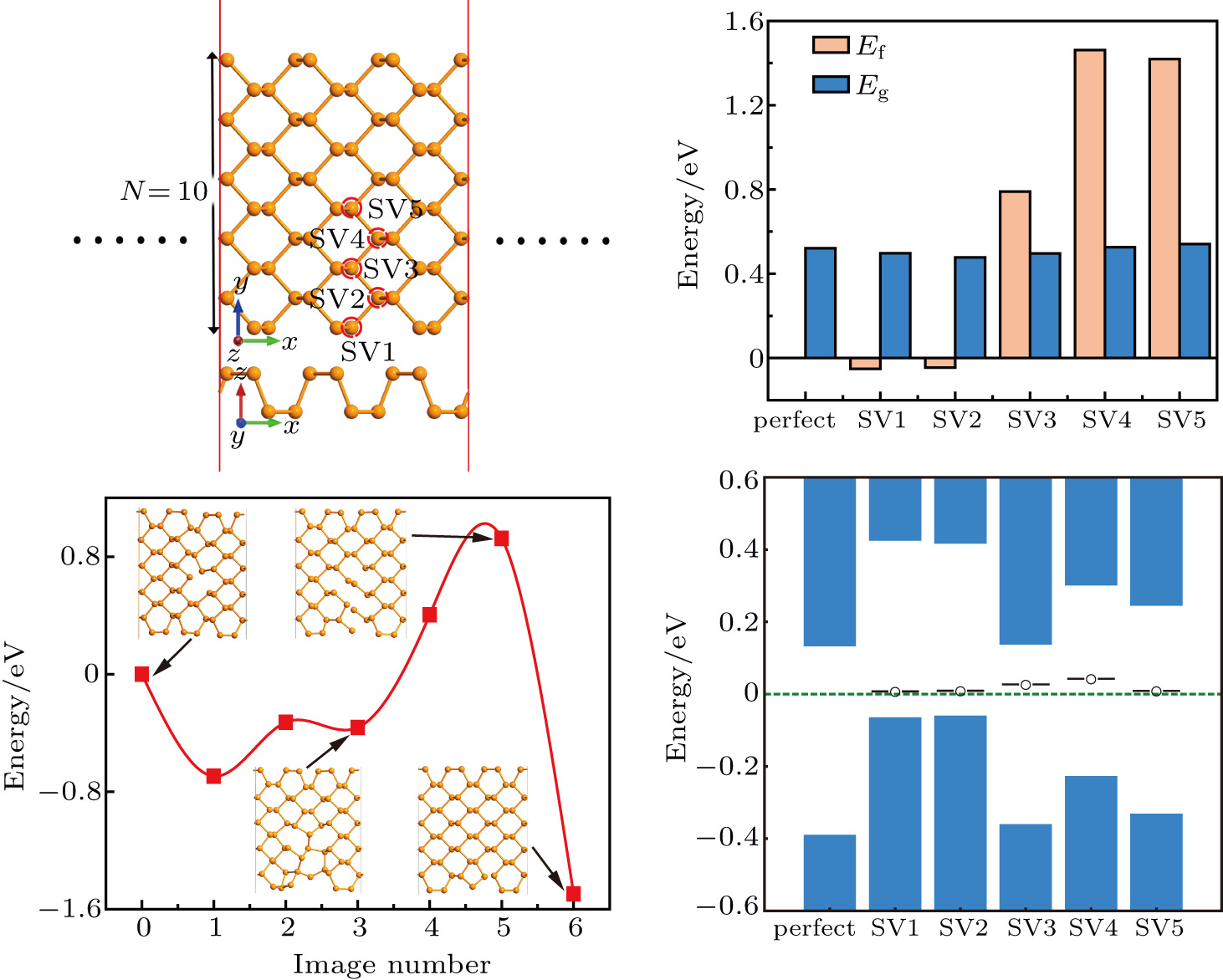
The configuration of an APNR is shown in Fig. 1(a). Notably, the nanoribbon width is marked by the atom number along the zigzag direction. In our case, the APNR with a width N = 10 of 15.37 Å and taking a total of 60 atoms of 5 × 3 × 1 supercell. Making x direction with periodicity, there is a 20 Å vacuum layer in both y and z directions to ensure non-interaction between adjacent supercell. The lattice parameter is a = 3.30 Å and b = 4.58 Å with the Cmca space group. In our calculation, the bandgap (Eg) of the perfect APNR with N = 10 is 0.53 eV, which is in agreement with the previous results.[45]

Fig. 1. (a) Top and side views of an APNR with single vacancies at different positions, (b) formation energy and bandgap of the defective APNR. (c) Diffusion barrier for the migration of SV5 to SV1. (d) VBM, CBM and DL with respect to the Fermi level of the defective APNR. The Fermi level is set to zero.

First of all, five non-equivalent single vacancies SV1–SV5, about 1.6% defect concentration, are introduced from the edge to the middle region. In order to estimate the favorite vacancy location, we calculate the formation energy in terms of the relationship

where Edefect and Eperfect are the total energies of defect and perfect structures, ni is the number of i atom, μi represents the chemical potential of the removed atom. In our case, μi is the energy of a single phosphorus atom in monolayer BP. In Fig. 1(b), the energies of SV1 and SV2 are negative, but the positive energies of SV4 and SV5 near the center are 1.46 eV and 1.42 eV, approximating to 1.62 eV of phosphorene.[35] Accordingly, it is indicated that the vacancy defect can be spontaneously formed in the edge region because of dangling bond with high activity. After structural relaxation, the SV1 and SV2 reconstruct a five-membered ring at the edge, but SV2 needs more energy to break the covalent bond. The cases of SV4 and SV5 have similar behaviors to that of monolayer BP.[35]

It should be noted that the vacancies are not stationary in APNRs. Therefore, the possible diffusion should be taken into account. We use the NEB approximation to calculate the activation energy of phosphorus vacancy migration pathway between SV5 and SV1. As shown in Fig. 1(c), the migration potential in the middle region is 0.3 eV, which is consistent with the case in BP.[36] However, when the defect migrates from edge to center, the barrier enhances a large value (1.0 eV), which means that the vacancies are hard to move inward. Therefore, the distribution of atomic vacancies is not random but tending to along the margin.[46] Figure 1(d) shows the energy band relative to the Fermi level with changing vacancy positions. Accounting for a small percentage of entire nanoribbon, the bandgaps of all imperfect APNRs are between 0.48 eV and 0.52 eV, which are slightly smaller than that of the perfect structure with 0.53 eV. However, the VBM and conduction band minimum (CBM) appear to significant shift compared to that of the perfect nanoribbon. Moreover, it is clear that the DL is generated and sensitive to the vacancy position.

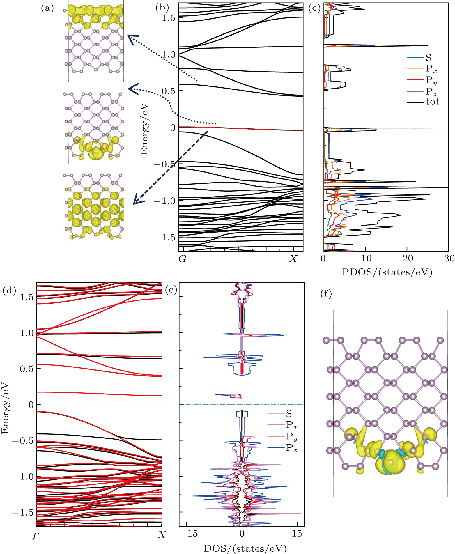
In order to obtain the deep understanding of vacancy effect, we calculate the partial differential charge, band structure and projected density of state (PDOS) in the case of SV1 with/without spin polarization, as shown in Figs. 2(a)2(e). Evidently, this type of APNR has an indirect bandgap like the perfect case, and the high symmetry points of VBM and CBM are Γ and X in the Brillouin zone regardless of spin polarization. When a single vacancy occurs, the total electron number is odd, resulting in the local DL passing through the Fermi level. It is obvious that the VBM, CBM and DL are mainly contributed by the pz orbital of phosphorus atoms in the intermediate, edge and adjacent defect regions, respectively. The overlap between charge density varies with the vacancy position, thus resulting in the band edge offset. Considering spin polarization, the DL presents spin splitting, and the nonmagnetic APNRs obtain a variable magnetic moment between 0.65μB and 1.04μB, which is dependent on the defect location. The spin projected state density exhibits imbalance between spin-up and spin-down states in the pz orbital. In addition, spin differential charge density is mainly localized around the defect sites as predicted in Fig. 2(f).

Fig. 2. (a) Partial charge densities of CBM, VBM and DL, (b) band structure, and (c) PDOS without spin-polarized, (d) band structure (spin up/down is represented by black/red), and (e) PDOS with spin polarized, (f) spin differential charge density of SV1-APNR, respectively.
3.2. Size-dependent electronic and transport properties of SV1-APNRs

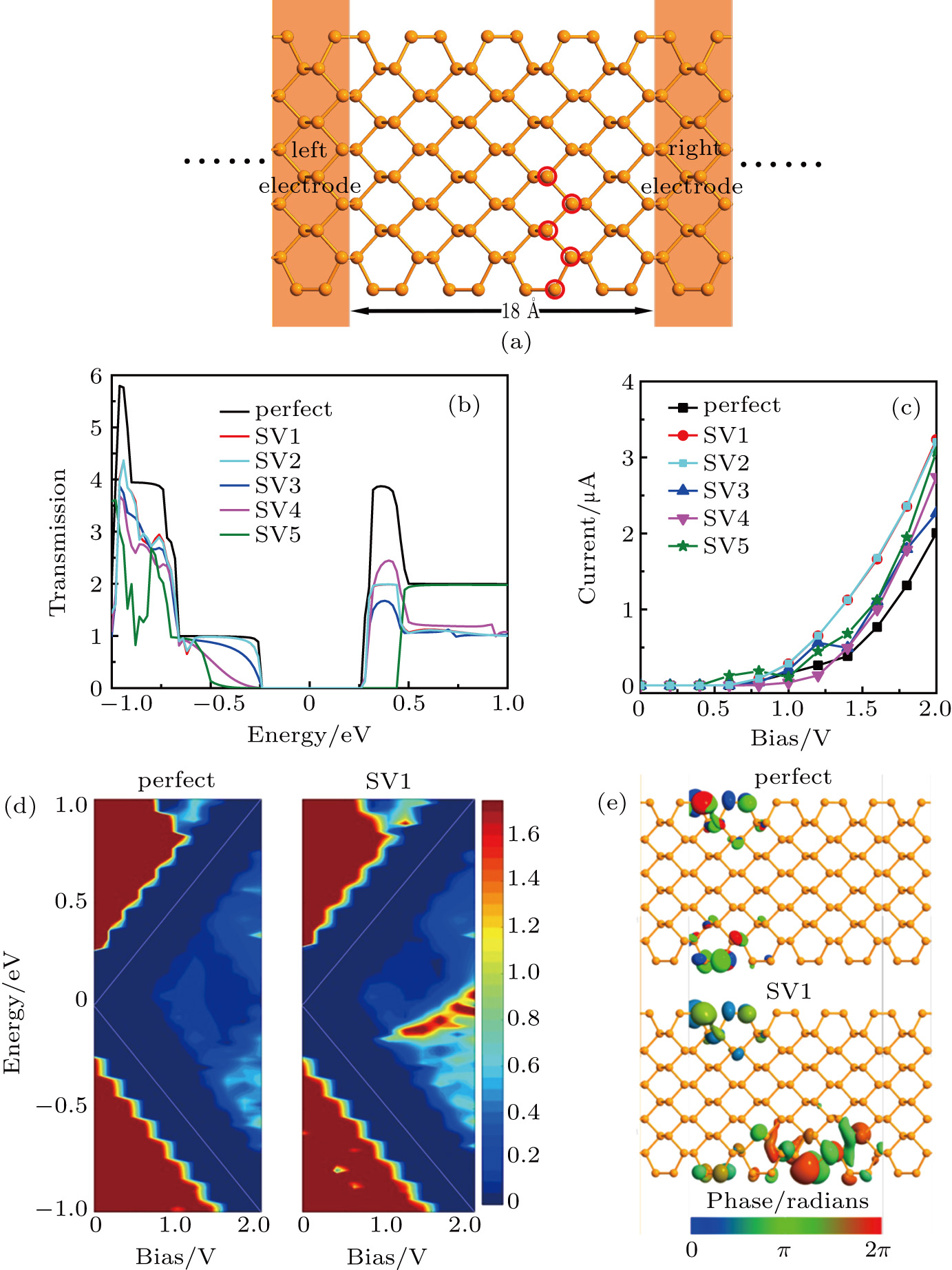
To investigate the electrical transport properties, we built a two-probe device as shown in Fig. 3(a). It includes three parts: left and right electrodes, as well as central scattering region. The scattering region contains a width of N = 10 and a length of 18 Å for a PNR. Defects are only introduced at the scattering region. The transmission coefficients under zero bias are given in Fig. 3(b).

Fig. 3. (a) The schematic illustration of a two-probe defective APNR device. (b) Transmission spectra under zero bias, (c) IV curves of pristine and defective APNR with SV1 to SV5. (d) Bias-dependent transmission spectrum, (e) transmission eigenstates in the scattering region under bias of 1.4 V in perfect and SV1-APNR.

Obviously, the perfect APNRs exhibit integer quantum transmission characteristics that the spectra consist of a series of steps in the range of high or low energy. However, when the vacancy defect appears and draws near the center region, the transmission coefficient of the low energy part declines and the integer quantum transmission disappears. All transmission gaps are approximately 0.5 eV. The DL is local so that it does not correspond to the transmission peak inside the bandgap. This phenomenon also referred as the Anderson localization.[39] Moreover, the IV curve is also an important characteristic of the electronic device (Fig. 3(c)). Interestingly, all configurations show the semiconductor behaviors. The turn-on voltages are corresponding to the bandgap with 0.5 V. Strikingly, the current of defective APNRs enhances from 1.2 to 1.5 times compared to that of the perfect counterparts.

In order to thoroughly analyze the phenomenon of current boost in the defective nanoribbons, we calculate bias voltage dependence of transmission spectrum (Fig. 3(d)). In contrast to perfect APNRs, we can see that SV1-APNRs possess a transmission peak within the plateau (red areas in the right triangle) in 0.14 V bias and −0.12 eV electron energy contributing by the DL. The transmission plateau extends toward the valence band, which is consistent with the p-type conductivity of APNRs. Moreover, eigenstates at the transmission peak are shown in Fig. 3(e). Clearly, the conduction in APNRs is mainly from the edge propagating mode. The incoming wave of eigenstates delocalizes at the left edge part in the perfect APNRs, while the ballistic and diffusive transport eigenstates covering the entire lower edge can be observed in the SV1 cases. Although the complex scattering modes occur near the vacancy, the complete channel is still formed at the high bias voltage. This is because the electron state in the two electrodes can match the DL in the scattering region.

In general, there are two ways to change the defect concentration in the DFT calculations: one is to expand or shrink the supercell, and the other is to introduce multiple vacancies. For the former, to explore the joint effect of nanoribbon size and defects, we select the SV1-APNRs with various widths possessing the lowest formation energy to study. Figures 4(a)4(c) plot the formation energy, the bandgap, the distribution of band levels and the net magnetic moment as a function of width. Evidently, the defect formation energy increases as the scale decreases, indicating that the wider nanoribbon has higher stability. Owing to the quantum confinement effect, the bandgap decreases from 0.8 eV of N = 6 to 0.4 eV of N = 14, which exhibits an N−2 relationship.[22] Magnetic moment is slightly reduced from 0.97μB to 0.90μB. The quasiflat DL passes through the Fermi level and the separation to the VBM drops from 0.53 eV to 0.07 eV. Therefore, the transform of deep-to-shallow acceptor level occurs in APNRs.

Fig. 4. (a) Formation energy and bandgap, (b) band edge and DL respect to Fermi level, and (c) net magnetic moment as a function of nanoribbon width.

Upon the transport behavior, the APNR devices with N = 6 to N = 10 containing SV1 defects are constructed to calculate the transmission spectrum under zero bias (Fig. 5(a)). Noticeably, the transmission gap is in line with the previous circumstance that the narrower nanoribbon has the larger gap. The vacancy scattering causes the integral steps smooth in the edge conductance, but the narrower APNRs have more sensitive to the edge vacancy. As shown in Fig. 5(b), the threshold of turn-on voltage and the current intensity are uniformly increased as the nanoribbon widens. Also, the APNR with N = 10 has the largest transmission peak in the bias window (Fig. 5(c)). In addition, the transmission peak formed by the DL under high bias is closer to VBM that exists in the wider APNRs. Therefore, the DL can be as an electron acceptor that becomes a bridge for electron exchanging. Also, the transmission plateau region becomes wider when the transformation of deep-to-shallow acceptor level occurs.

Fig. 5. (a) Transmission spectra at zero bias, (b) IV curves, (c) bias-dependent transmission spectra of APNR with N of 6–10.
3.3. The case of APNRs with multiple vacancies

Unlike changing the supercell size to adjust defect concentration, we should consider the interaction between vacancies in APNRs with multiple vacancies. Based on the structure of SV1-APNRs with N = 10, we construct a series of APNRs with double vacancies about defect concentration of 3.2% at identical edge (DsV1–4) or different edges (DdV1–5) (Fig. 6(a)). Figure 6(b) shows the related formation energies and bandgaps. Notably, for the single edge defect ribbons, the formation energy of DsV1-APNR (−0.25 eV) is the minimum, which is smaller than that of SV1-APNR. The bandgaps can be affected when changing the separation of vacancies in DsV-APNRs. In this case, the DLs do not appear. The origin is that the vacancy pair will relax and the sublattice symmetry of DsV-APNRs will preserve (Fig. 6(c)).[39] In contrast, DdV can be regarded as the combination of two SV1 defects. However, the bandgap increases from original 0.48 eV to 0.70 eV and two DLs appear near the VBM. Moreover, for the cases of three vacancies in the same (TsV1) and different edges (TdV1), only one DL can be found in the gap. As shown in Table 1, the independent vacancies can produce magnetism which is proportional to the number of defects. However, if the vacancies are close to each other, the lattice will undergo local reconstruction, causing the reduction or even the disappearance of magnetism in the multiple vacancy system. This illustrates that the sublattice symmetry is strongly associated with the number of defects and partial relaxation.

Fig. 6. (a) Structure of multiple vacancies of APNR, (b) formation energy and bandgap, as well as (c) band edges and DL with respect to the Fermi level of APNR with different multiple vacancies.
Table 1.

The magnetic moment of different defect types in APNRs.

.

In Fig. 7(a), the IV characteristics of DsV1-, DdV1-, TsV1-, and TdV1-APNR devices are calculated by NEGF. It is clear that DdV1 has a larger effect on the conductance. Even though DdV1-APNR has the largest transport gap, the conductance is the strongest compared with other structures owing to more DLs in the gap. Figure 7(b) shows the transmission spectrum as a function of voltage. Obviously, when the defects distribute at different edges, the electron transmission in the upper triangular is drastically reduced due to the disappearance of edge transmission channels. However, the portion of conduction band transmission outside the bias window has less effect to the current. In contrast to other ribbons, DdV1-APNR has a higher and wither transmission plateau in the bias window.[40,47] Unlike the conventional expectation, except for bandgap and effective mass, the transport properties can also be determined by the number of DLs that can be modulated by the defect concentration.

Fig. 7. (a) The IV curves of APNR with various multiple vacancies, (b) bias-dependent transmission spectra of DsV1-, TsV1-, DdV1- and TdV1-APNRs, respectively.
4. Conclusion

In summary, using the density functional theory and non-equilibrium Green’s function, we investigate the electronic and transport properties of one-dimensional defective APNRs. It is revealed that vacancies prefer to trap in the edge region owing to low formation and high diffusion barrier. All single vacancies introduce a local defect state near the VBM with 0.9μB magnetic moment originally from pz orbital, which enhances transport current by 1.2–1.5 times. The structure instability, magnetic moment and bandgap are reduced when the width increases. Notably, the DL takes a deep-to-shallow transformation that can improve the electrical transport performance. Moreover, the number of DL is an important factor for transport, showing a dependence on edge notch and edge reconstruction in the APNRs with multiple vacancies. Therefore, defect engineering is an effective method to improve electronic and transport properties of APNRs and can also be applying for the relevant applications.

Reference
[1] Woomer A H Farnsworth T W Hu J Wells R A Donley C L Warren S C 2015 ACS Nano 9 8869
[2] Li L Yu Y Ye G J Ge Q Ou X Wu H Feng D Chen X H Zhang Y 2014 Nat. Nanotechnol. 9 372
[3] Xia F N Wang H Jia Y C 2014 Nat. Commun. 5 4458
[4] Liang L Wang J Lin W Sumpter B G Meunier V Pan M 2014 Nano Lett. 14 6400
[5] Buscema M Groenendijk D J Blanter S I Steele G A van der Zant H S J Castellanos-Gomez A 2014 Nano Lett. 14 3347
[6] Priydarshi A Chauhan Y S Bhowmick S Agarwal A 2018 Phys. Rev. 97 115434
[7] Kumar P Bhadoria B S Kumar S Bhowmick S Chauhan Y S Agarwal A 2016 Phys. Rev. 93 195428
[8] Lei W Liu G Zhang J Liu M 2017 Chem. Soc. Rev. 46 3492
[9] Zhang P Wang J Duan X M 2016 Chin. Phys. 25 037302
[10] Zhang Z Ouyang G 2018 ACS Appl. Energy Mater. 1 5675
[11] Nourbakhsh Z Asgari R 2016 Phys. Rev. 94 035437
[12] Pang J Bachmatiuk A Yin Y Trzebicka B Zhao L Fu L Mendes R G Gemming T Liu Z Rummeli M H 2018 Adv. Energy Mater. 8 1702093
[13] Li X Wang X Zhang L Lee S Dai H 2008 Science 319 1229
[14] Vierimaa V Krasheninnikov A V Komsa H P 2016 Nanoscale 8 7949
[15] Wu Q Shen L Yang M Cai Y Huang Z Feng Y P 2015 Phys. Rev. 92 035436
[16] Yagmurcukardes M Peeters F M Senger R T Sahin H 2016 Appl. Phys. Rev. 3 041302
[17] Li Y Zhou Z Zhang S Chen Z 2008 J. Am. Chem. Soc. 130 16739
[18] Watts M C Picco L Russell-Pavier F S Cullen P L Miller T S Bartus S P Payton O D Skipper N T Tileli V Howard C A 2019 Nature 568 216
[19] Maity A Singh A Sen P Kibey A Kshirsagar A Kanhere D G 2016 Phys. Rev. 94 075422
[20] Zhang J Liu H J Cheng L Wei J Liang J H Fan D D Shi J Tang X F Zhang Q J 2015 Sci. Rep. 4 6452
[21] Fan Z Q Sun W Y Jiang X W Luo J W Li S S 2017 Org. Electron. 44 20
[22] Liu Y Bo M Yang X Zhang P Sun C Q Huang Y 2017 Phys. Chem. Chem. Phys. 19 5304
[23] Li W Zhang G Zhang Y W 2014 J. Phys. Chem. 118 22368
[24] Dong M M Wang Z Q Zhang G P Wang C K Fu X X 2019 Phys. Chem. Chem. Phys. 21 4879
[25] Liao C W Zhao Y P Ouyang G 2018 ACS Omega 3 14641
[26] Poljak M Suligoj T 2018 IEEE Trans. Electron. Dev. 65 290
[27] Farooq M U Hashmi A Hong J 2015 ACS Appl. Mater. Inter. 714423
[28] Guo C Wang T Xia C Liu Y 2017 Sci. Rep. 7 12799
[29] Si C Choe D Xie W Wang H Sun Z Bang J Zhang S 2019 Nano Lett. 19 3612
[30] Wang Y Pham A Li S Yi J 2016 J. Phys. Chem. 120 9773
[31] Srivastava P Hembram K P Mizuseki H Lee K R Han S S Kim S 2015 J. Phys. Chem. 119 6530
[32] Chintalapati S Lei S Xiong Q Yuan P F 2015 Appl. Phys. Lett. 107 072401
[33] Sha Z D Pei Q X Zhang Y Y Zhang Y W 2016 Nanotechnology 27 315704
[34] Riffle J V Flynn C Laurent B S Ayotte C A Caputo C A Hollen S M 2018 J. Appl. Phys. 123 044301
[35] Hu W Yang J 2015 J. Phys. Chem. 119 20474
[36] Cai Y Ke Q Zhang G Yakobson B Zhang Y 2016 J. Am. Chem. Soc. 138 10199
[37] Gaberle J Shluger A L 2018 Nanoscale 10 19536
[38] Xie F Fan Z Zhang X Liu J Wang H Liu K Yu J Long M 2017 Org. Electron. 42 21
[39] Yuan S Rudenko A N Katsnelson M I 2015 Phys. Rev. 91 115436
[40] Poljak M Suligoj T 2016 Nano Res. 9 1723
[41] Kresse G Furthmüller J 1996 Phys. Rev. 54 11169
[42] Naemi Z Tafreshi M J Salami N Shokri A 2019 J. Mater. Sci. 54 7728
[43] Sheppard D Xiao P Chemelewski W Johnson D D Henkelman G 2012 J. Chem. Phys. 136 074103
[44] Buttiker M Imry Y Landauer R Pinhas S 1985 Phys. Rev. 31 6207
[45] Qiao J Kong X Hu Z X Yang F Ji W 2014 Nat. Commun. 5 4475
[46] Das P M Danda G Cupo A et al. 2016 ACS Nano 10 5687
[47] Li L L Peeters F M 2018 Phys. Rev. 97 075414