Improved interfacial properties of HfGdON gate dielectric Ge MOS capacitor by optimizing Gd content
Zhou Lin1, Liu Lu1, Deng Yu-Heng1, Li Chun-Xia2, Xu Jing-Ping1, †
School of Optical and Electronic Information, Huazhong University of Science and Technology, Wuhan 430074, China
Shenzhen Institute of Information Technology, Shenzhen 518172, China


† Corresponding author. E-mail: jpxu@hust.edu.cn

Project supported by the National Key Research and Development Program of China (Grant No. 2018YFB2200500) and the National Natural Science Foundation of China (Grant Nos. 61851406 and 61274112).

Abstract

High-quality dielectric/Ge interface and low gate leakage current are crucial issues for high-performance nanoscaled Ge-based complementary metal–oxide–semiconductor (CMOS) device. In this paper, the interfacial and electrical properties of high-k HfGdON/LaTaON stacked gate dielectric Ge metal–oxide–semiconductor (MOS) capacitors with different gadolinium (Gd) contents are investigated. Experimental results show that when the controlling Gd content is a suitable value (e.g., ∼ 13.16%), excellent device performances can be achieved: low interface-state density (6.93 × 1011 cm−2 · eV−1), small flatband voltage (0.25 V), good capacitance–voltage behavior, small frequency dispersion, and low gate leakage current (2.29× 10⁻⁶ A/cm2 at Vg = Vfb + 1 V). These could be attributed to the repair of oxygen vacancies, the increase of conduction band offset, and the suppression of germanate and suboxide GeOx at/near the high k/Ge interface by doping suitable Gd into HfON.

1. Introduction

Recently, it has become increasingly difficult in further scaling down the geometric dimension of Si-based metal–oxide–semiconductor field-effect transistor (MOSFET). For overcoming the obstacle, Ge-based and III–V compound semiconductor-based MOSFETs (e.g., GaN-HEMTs) with high-k gate dielectric have been extensively studied to further improve the scaled CMOS technology due to their higher electron and/or hole mobilities than those of silicon.[16] For Ge MOS, unstable and water-soluble GeOx (x < 2) degrades the Ge/gate-dielectric interface quality, resulting in poor electrical properties,[7] which has hampered the development of Ge MOSFET. In order to solve this problem, different surface passivation layers, such as LaTaON,[8] ZrON,[9] NbSiON,[10] etc.[1114] have been investigated and exhibited good interface quality in the presence of Ge. On the other hand, Hf-based oxide has been considered as one of the most promising high-k materials and used as gate dielectric due to its high k value (∼ 25) and large band gap (∼ 5.8 eV).[15,16] However, it has been found that the electrical properties of the device will be degraded due to intermixing between Ge and Hf.[1,2,714] Although the incorporation of nitrogen (N) into HfO2 could suppress Ge and O diffusion and improve the interfacial property,[17,18] it reduced the valence- and conduction-band offsets.[19] Fortunately, some recent investigations have demonstrated that the Gd-doped HfO2 can increase the conduction-band offset and transform HfO2 from the monoclinic phase to the cubic phase, thus diminishing the leakage, improving the interface quality, and also augmenting the k value of dielectric.[20,21] So in this work, the effects of Gd content in HfGdON gate dielectric on interface and electrical properties of Ge MOS devices with LaTaON interlayer are further investigated so that Gd content is optimized to obtain high-quality dielectric/Ge interface and excellent device performances.

2. Experiments

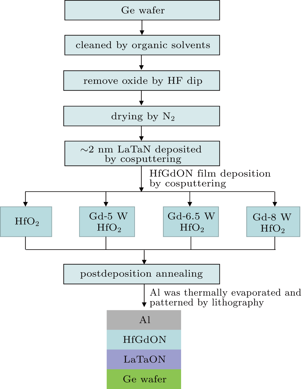
Ge MOS capacitors were fabricated on (100) n-type Ge wafers with a resistivity of 0.02 Ω · cm–0.1 Ω · cm. The wafers were cleaned by using ethanol, acetone, and trichloroe-thylenein in sequence, followed by dipping them in diluted HF (1:50) for 30 s, and then rinsed with deionized water for several cycles to remove the native oxide. After drying by N2, the wafers were transferred immediately to the vacuum chamber of a sputtering system. Before deposition, the vacuum chamber was evacuated to a base pressure of 5.0 × 10⁻⁴ Pa. A ∼ 2-nm LaTaN film was deposited by cosputtering of La target and Ta target at room temperature in an Ar/N2 (= 15/6) ambient atmosphere, followed by an in-situ deposition of ∼ 8-nm HfGdON film by cosputtering of HfO2 target and Gd target in the same ambient. The Gd content was adjusted by changing the Gd-target power as shown in Fig. 1. Then, a postdeposition annealing (PDA) was carried out in N2 (500 sccm)+O2 (50 sccm) ambient atmosphere at 500 °C for 5 min to convert LaTaN into LaTaON and reduce the oxygen vacancy in HfGdON film. The Al was thermally evaporated and patterned by lithography, and used as a gate electrode with an area of 7.85 × 10⁻⁵ cm2. Finally, postmetallization annealing was carried out in a forming gas (95% N2 + 5% H2) at 300 °C for 20 min.

Fig. 1. Process flow chart of Ge MOS capacitor with gate stacked dielectric of HfGdON/LaTaON/Ge.

High-frequency (HF, 1 MHz) capacitance–voltage (CV) and gate leakage current density versus gate voltage (JgVg) characteristics were measured by HP4284A precision LCR meter and Keithley 4200-SCS semiconductor parameter analyzer respectively under a light-tight and electrically-shielded condition at room temperature. The physical thickness of the gate dielectric was determined by a spectroscopic ellipsometer. The x-ray photoelectron spectroscopy (XPS) was employed to investigate the compositions and chemical states of the samples.

3. Results and discussion

The compositions and chemical states of four samples with different Gd contents (from 0 to 45%, as analyzed below) are investigated by etching the HfGdON gate dielectrics to a thickness of ∼ 4 nm from the Ge surface using an in-situ Ar+ ion beam in the XPS chamber. The binding energy is calibrated by centering the Ge 3d at 28.8 eV, and all peaks have their own fixed full wide at half maximum (FWHM). Firstly, the spectrum of La 3d is shown in Fig. 2(a), and two strong peaks at 851.40 eV (La 3d3/2) and 834.50 eV (La 3d5/2) are detected. The spin–orbit splitting energy of 16.9 eV is in a good accordance with that of La2O3/LaON, and the La 3d3/2 peaks related to La2O3 are located in a binding-energy range of 834.2 eV–837.0 eV,[21] confirming the presence of La2O3/LaON in the interlayer. The spectrum of Ta 4f is shown in Fig. 2(b), in which two strong peaks are located at 26.18 eV (Ta 4f7/2) and 28.01 eV (Ta 4f5/2), respectively. The spin–orbit splitting energy is 1.83 eV, which is close to a standard value of 1.9 eV, indicating the presence of Ta5+ from Ta2O5/TaON.[22]

Fig. 2. XPS spectrum of HfGdON/LaTaON/Ge MOS with Gd content of ∼ 13.16% for (a) La 3d and (b) Ta 4f. Other samples with Gd incorporation have similar results.

The Gd 4d core-level spectrum is shown in Fig. 3(a), and two strong peaks of Gd 4d3/2 (∼ 147.47 eV) and Gd 4d5/2 (∼ 142.43 eV) are detected, which can be fitted well by spin–orbit splitting energy of about 5.0 eV, confirming the formation of Gd2O3/GdON.[23] In addition, an extra peak (∼ 140.65 eV) can be observed, which can be attributed to the electrostatic interaction between Gd 4d core level and a partially filled Gd 4f level because Gd belongs to the heavy lanthanide group element.[24] Figure 3(b) is the N 1s spectrum, showing the incorporation of nitrogen into the gate dielectric film.
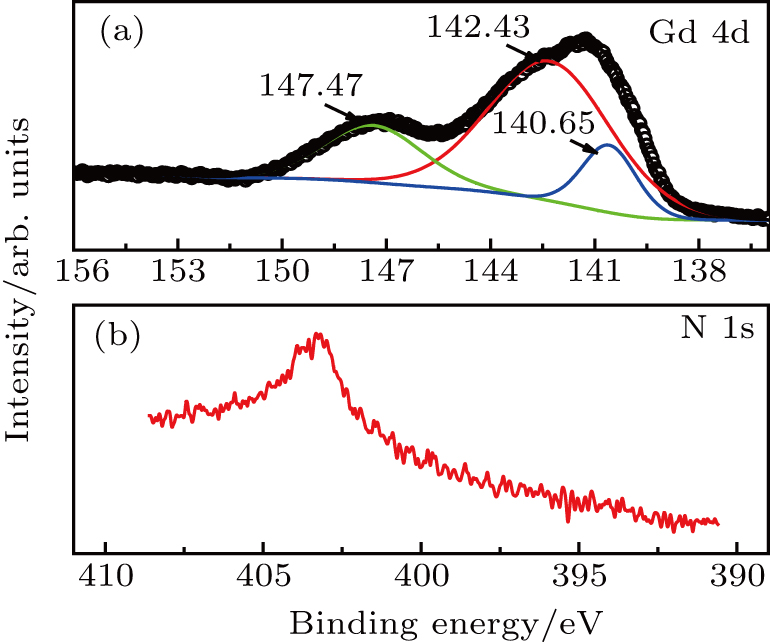
Fig. 3. XPS spectra of HfGdON/LaTaON/Ge MOS with Gd content of ∼ 13.16% for (a) Gd 4d and (b) N 1s. Other Gd-doped samples have similar results.

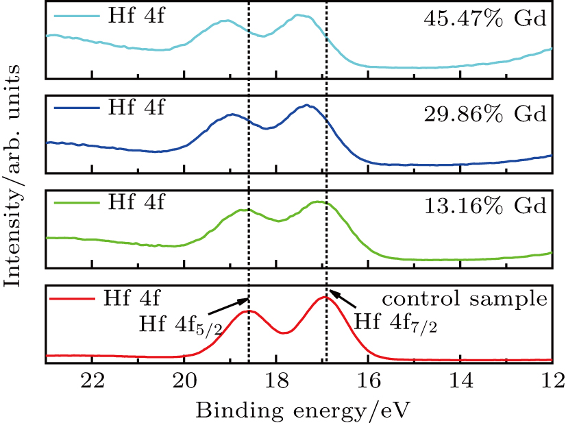
Figure 4 demonstrates the core-level spectra of Hf 4f, and all of them are deconvoluted into two peaks of Hf 4f5/2 and Hf 4f7/2, which are in accordance with spin–orbit splitting energy of about 1.7 eV.[2527] From the above XPS results, it can be suggested that the HfGdON dielectric film is formed. By calculating the peak-area ratio of Gd 4d to Hf 4f for each of the three Gd-doped samples, their Gd content values [Gd/(Gd+Hf)] are obtained to be 13.16%, 29.86%, and 45.47%, respectively. Compared with the control sample without doping Gd, the sample with the Gd content of ∼ 13.16% possesses a 0.2-eV binding energy shift of the Hf 4f peak, which, obviously, is caused by the incorporation of gadolinium into HfON film. As the Gd/(Gd+Hf) atomic ratio increases, the Hf 4f peaks shift to higher binding energy, which is consistent with the results in Refs. [28] and [29] and can be attributed to the suppression of oxygen vacancies by doping Gd, to reduce the local electronic density of states.[20,28,30]

Fig. 4. XPS spectra of Hf 4f for four samples with (a) 0% Gd, (b) 13.16% Gd, (c) 29.86% Gd, and (d) 45.47% Gd.

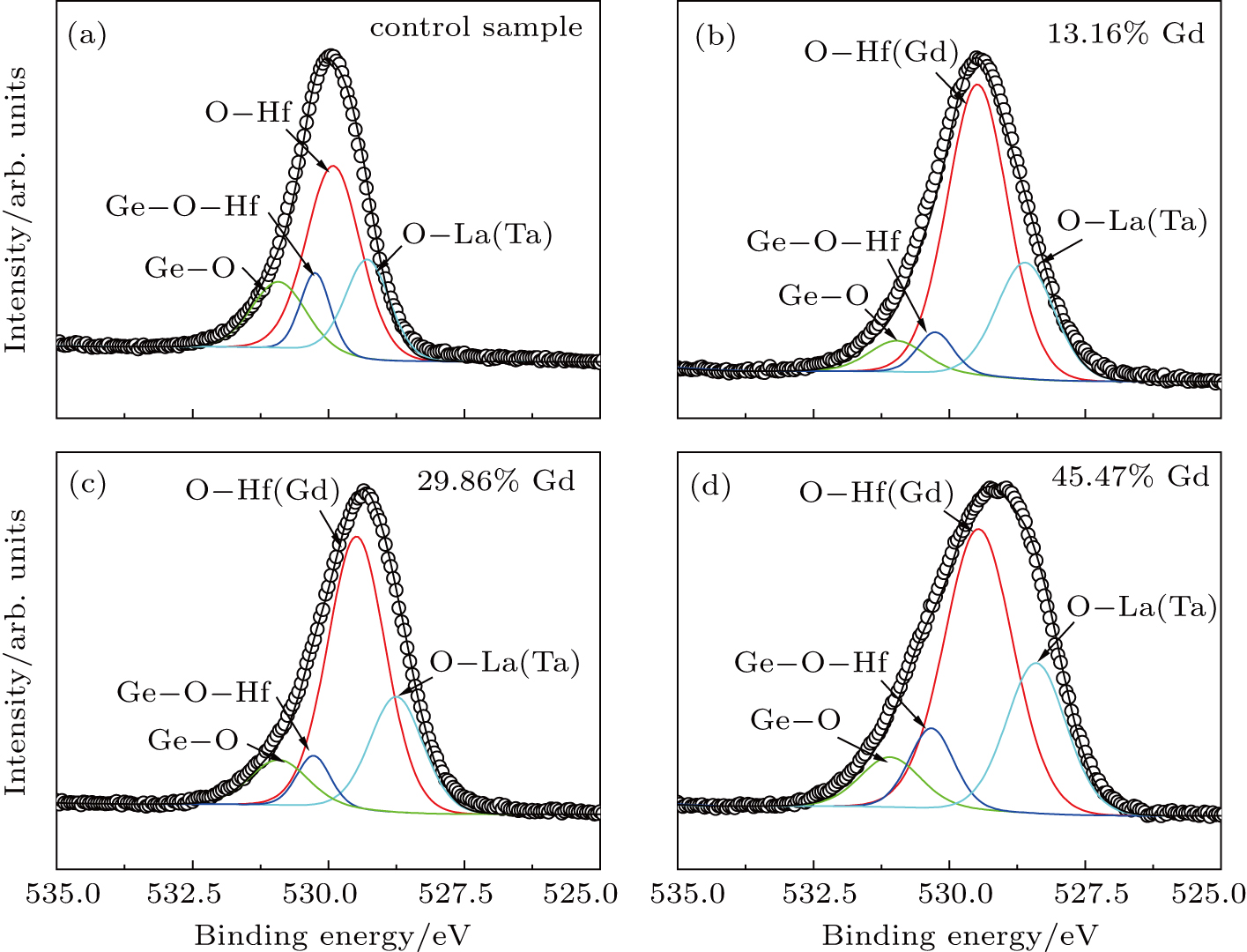
Because of a strong overlap between the Ge 3d peak and Hf or Ta peak,[8,31] the Ge 2p3/2 core level spectrum for each of four samples is used to investigate interfacial quality between the high-k stack and Ge substrate as shown in Fig. 5. The peaks from GeO2, GeOx, and Ge substrates are found to be located at 1221.1 eV, 1218.8 eV, and 1217.5 eV,[32] respectively. For the Gd-doped samples, a peak with a binding energy (BE) value of 1216.2 eV is observed, which belongs to Gd 3d3/2 whose BE value is between 1212 eV and 1227 eV.[33] A peak with a BE value of 1219.9 eV in Fig. 4(a) originates from HfGeOx, which is formed due to the Hf and O diffusing onto the surface of Ge substrate during the 500-°C PDA.[34] The O 1s core level spectra of four samples in Fig. 6 further confirm the formation of HfGeOx and Ge suboxides as indicated by the Ge–O–Hf and O–Ge peaks, respectively. The HfGeOx peak has a positive shift of BE (ΔBE = 2.40 eV) relative to the peak of the Ge substrate as shown in Fig. 5(a). Obviously, as Gd content increases from 0 to 13.16%, this shift decreases (ΔBE = 1.76 eV), indicating the suppression of the Hf diffusion by Gd incorporation. However, as Gd content increases to higher values, a turnaround of ΔBE occurs, indicating the augment of the germanate due to the distortion of crystal structure by excessive Gd incorporation (29.86% and 45.47%).[35] To further analyze the effects of Gd doping, the area ratios of Ge suboxide to Ge 2p peak for four samples are calculated to be 12.06%, 5.39%, 7.72%, and 10.85%, corresponding to the samples with Gd content increasing from 0% to 45.47% respectively, implying that the formation of the unstable GeOx can greatly be suppressed due to an effective blocking role of Gd against O diffusion for the sample with Gd content of 13.16%, and however, with the incorporation of excessive Gd, e.g., 29.86%, even 45.47%, the peak area ratio of GeOx gradually increases and the interface quality is degraded due to the increased O diffusion. The peak intensity of the O–Ge bond in O 1s XPS spectra presents the same change trend in Fig. 6.
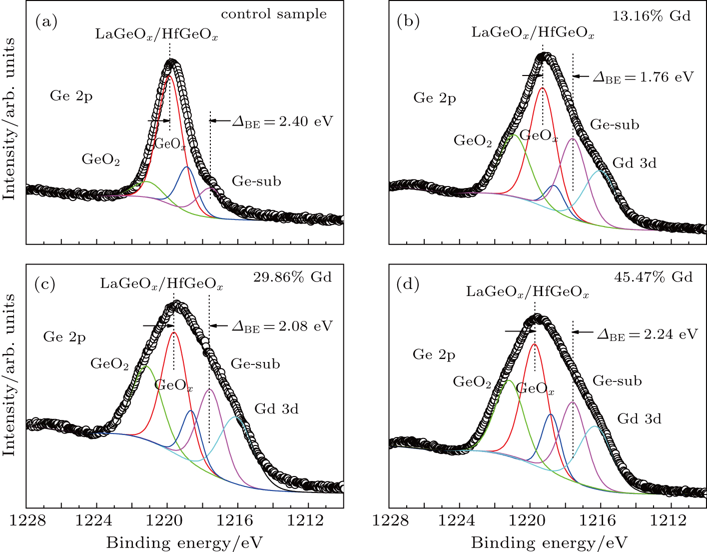
Fig. 5. XPS spectra of Ge 2p for four samples with (a) 0% Gd, (b) 13.16% Gd, (c) 29.86% Gd, and (d) 45.47% Gd.
Fig. 6. XPS spectra of O 1s for four samples with (a) 0% Gd, (b) 13.16% Gd, (c) 29.86% Gd, and (d) 45.47% Gd.

Based on the above XPS analyses, it can be suggested that the incorporation of an appropriate amount of Gd into HfON can suppress the formation of germanate and suboxide GeOx, and however, excessive Gd incorporation into HfON will be counterproductive. So it is important to control the Gd content entering into HfON for the purpose of improving the interfacial quality between HfGdON dielectric and Ge substrate.

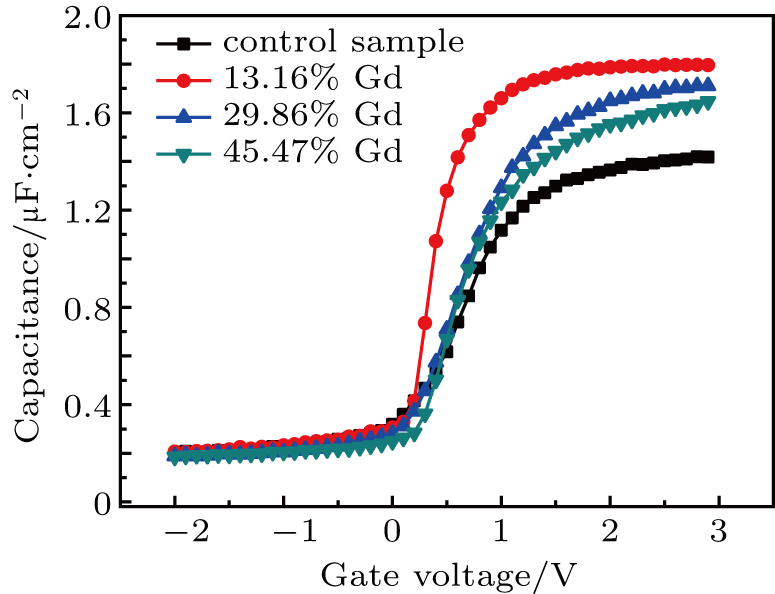
Figure 7 demonstrates the typical HF CV curves of the control sample (HfON) and three HfGdON samples. Apparently, the control sample has a much smaller accumulation capacitance (Cox) than those HfGdON samples, indicating that the incorporation of Gd into the HfON dielectric can increase its permittivity (k). The increased k value is attributed to the transformation of crystal structure wherein Gd3+ replaces a part of Hf4+. As is well known, the ionic radius of Gd3+ (∼ 0.105 nm) is slightly larger than that of Hf4+ (∼ 0.08 nm), which increases the length of the anion–cation bond, resulting in the enhancement of the molecular polarizability.[36]

Fig. 7. Typical HF CV curves of four samples with different amounts of Gd.

The permittivity can be calculated from[37] k = (1+8π am/3Vm)/(1 − 4π am/3Vm) where am denotes the molecular polarizability and Vm is the molecular volume. Obviously, the k value of HfGdON dielectric increases with the molecular polarizability increasing. In addition, the k value of the monoclinic HfO2 is lower than that of the cubic HfO2. With the Gd incorporation, the content of longer O–Gd bond increases as confirmed by the XPS spectrum of O 1s, and the monoclinic HfO2 is transformed into the cubic HfO2 due to substitution of O–Gd for O–Hf,[20] which plays a role in increasing k value too. But the k value will not always increase with the Gd content increasing as demonstrated by the measured results. The extracted electrical parameters from the CV curves are listed in Table 1. The equivalent k value of the gate dielectric is calculated from k = Cox tox/εA, where tox is the thickness of gate dielectric and A is the area of capacitor. The value of Vfb is determined by the flat-band capacitance,[38] and the oxide-charge density (Qox) is calculated from Qox = −Cox(Vfbϕms)/q, where ϕms is the work-function difference between Al and Ge. The interface-state density near midgap (Dit) is estimated by the Terman’s method.[39] Obviously, the k value increases firstly and decreases then as the Gd content increases, and reaches a maximum value (∼ 20.5) for Gd content of ∼ 13.16%. the k value for the samples decreasing with excessive Gd doping can be attributed to lower permittivity of the pure Gd2O3 than that of HfO2.

Table 1.

Electrical and physical parameters extracted from the HF CV curve of four samples.

.

The hysteresis behaviors of the CV curves for the four samples are presented in Fig. 8. To quantify their differences, the hysteresis voltages are calculated each as an averaged value between 0 V and 1 V, which, specifically,are 168 mV, 13 mV, 17 mV, and 20 mV for the samples with increasing Gd content. Compared with the control sample, the Gd-doped samples exhibit small hysteresis, implying a low density of defects in the LaTaON IPL and near/at the HfGdON/LaTaON interface due to the suppression of oxygen vacancies by doping Gd.[35] But for excessive Gd content, the crystal structure is distorted, resulting in the formation of more germinate and GeOx near/at the high-k/Ge interface due to enhanced diffusion of Hf and O towards the Ge surface as confirmed by the above XPS analyses, thus increasing hysteresis.
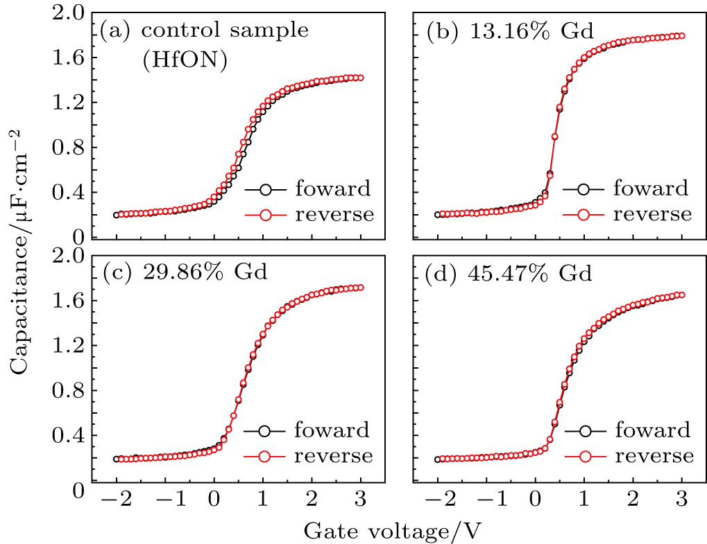
Fig. 8. Hystereses of CV curves for four samples with (a) 0% Gd, (b) 13.16% Gd, (c) 29.86% Gd, and (d) 45.47% Gd.

To further illustrate the interface quality of the samples, the frequency dispersions of the CV curves for the four samples are shown in Fig. 9. Once again, the sample with Gd content of ∼ 13.16% exhibits the smallest frequency dispersion, and as Gd content increases, the frequency dispersion gradually becomes bigger due to the same causes as the above, indicating the excellent interface quality for the 13.16%-Gd sample, which is further supported by its smallest Dit as listed in Table 1.
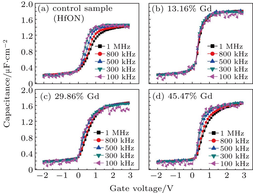
Fig. 9. Frequency dispersion of CV curves for four samples with (a) 0% Gd, (b) 13.16% Gd, (c) 29.86% Gd, and (d) 45.47% Gd.

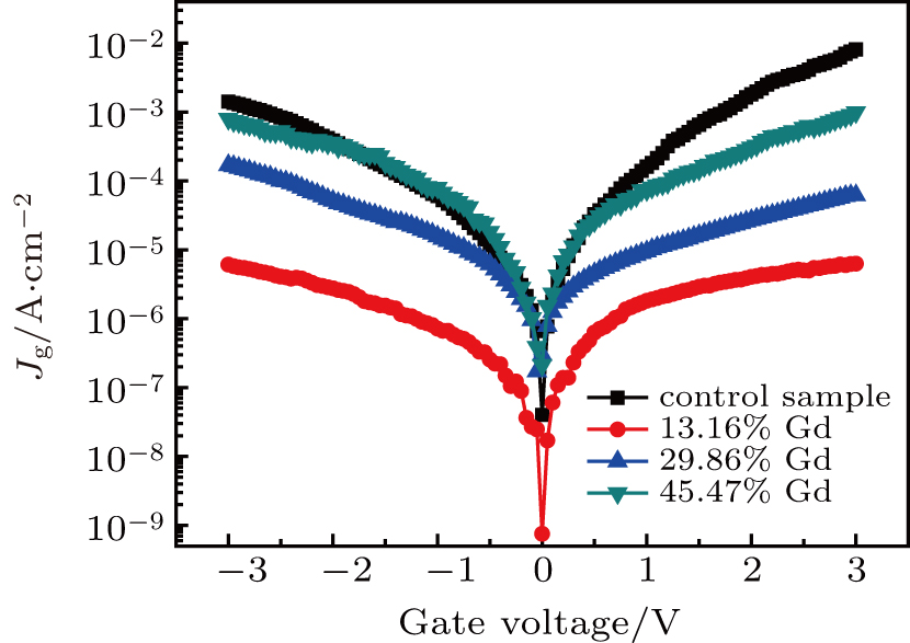
Figure 10 shows typical gate leakage properties of the four samples. The leakage current densities of all the Gd-doped samples are lower than that of the control sample due to the increase of conduction-band offset (ΔEc)[20] and the decrease of oxygen vacancies in the HfGdON film to different amounts. Furthermore, the lower electronegativity (∼ 1.2) and larger ionic radius (∼ 0.105 nm) of Gd3+ also contribute to the decrease of leakage current for the Gd-doped samples. However, the quantity of Gd3+ substitution for Hf4+ increases with Gd content increasing, which causes lattice to distort. Consequently, the 13.16%-Gd sample has the lower gate-leakage current than other Gd-doped samples (e.g., at Vg = Vfb + 1 V, Jg = 5.73 × 10⁻⁴ A/cm2, 2.29 × 10⁻⁶ A/cm2, 1.39 × 10⁻⁵ A/cm2, and 1.38 × 10⁻⁴ A/cm2 for the samples with increasing Gd contents respectively, as listed in Table 1), which is ascribed to its better interface quality and suppressed formation of Ge suboxide as confirmed by the above XPS analyses.

Fig. 10. Plots of gate leakage current density versus gate voltage for four samples.

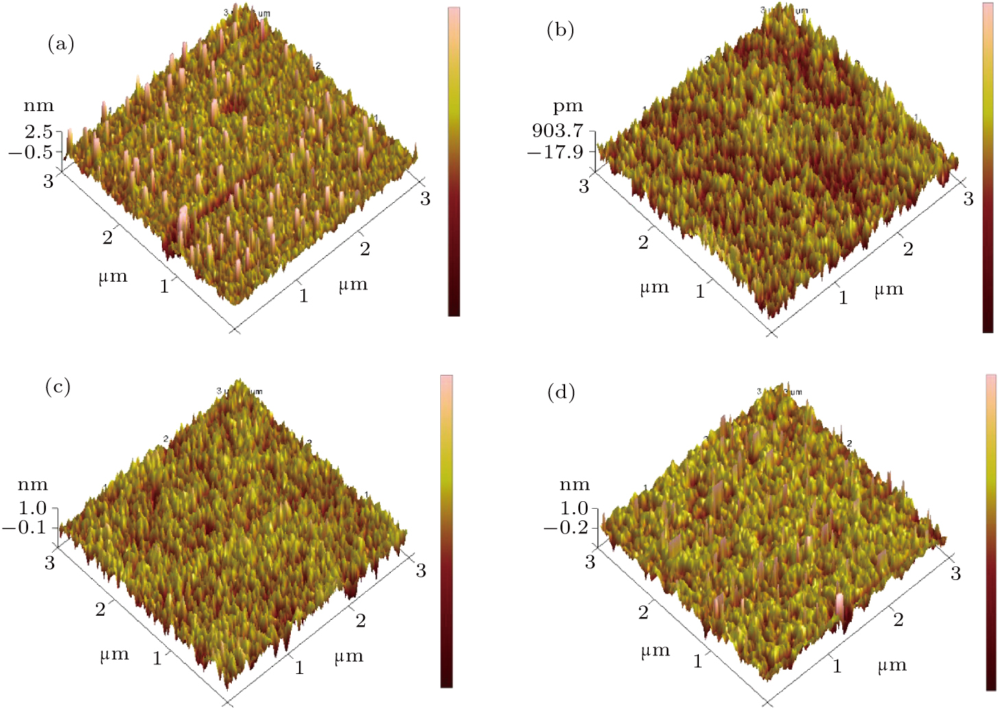
In addition, the AFM images of the gate–dielectric surface of all the samples are shown in Fig. 11. The root-mean-square (RMS) values of their surface roughness are 0.544, 0.206, 0.23, and 0.437 for the control sample and the samples with Gd contents of 13.16%, 29.86%, and 45.47%, respectively. With Gd incorporation, the HfGdON surface becomes smoother, but the excessive Gd incorporation generates the larger lattice strain in HfGdON due to substitutional increase, leading to larger RMS value. In fact, there is a one-to-one correspondence between the surface roughness and the gate leakage current or interface-state density, as shown by the above experimental results.

Fig. 11. AFM images of gate–dielectric surface for four samples with (a) 0% Gd, (b) 13.16% Gd, (c) 29.86% Gd, and (d) 45.47% Gd.
4. Conclusions

In summary, the effects of the Gd content in HfGdON gate dielectric on interfacial and electrical properties of the Ge MOS capacitor with LaTaON as interlayer are investigated. It is found that reasonable Gd incorporation in HfON (e.g., ∼ 13.16% Gd) exhibits superior interfacial and electrical properties, which is due to the formation of less germanate and the suppression of unstable Ge suboxides. Furthermore, the Gd-doped HfON can obtain larger conduction band offset (ΔEc) and effectively suppress the formation of oxygen vacancies, which contributes to small gate leakage current (2.29 × 10⁻⁶ A/cm2 at Vg = Vfb + 1 V) and low interface-state density (6.93 × 1011 cm−2 ·eV−1) for the 13.16%-Gd sample. However, when excessive Gd is incorporated, the performance of the device is deteriorated due to the distortion of crystal structure and poor interface quality. For Gd content below 13.16%, it deserves to further investigate their effects on device performances for determining the optimal Gd content in the gate stacked dielectric of HfGdON/LaTaON, and thus achieving more excellent electrical performance of Ge MOS device.

Reference
[1] Chi On C Kim H Chi D McIntyre P C Saraswat K C 2006 IEEE T. Electron Dev. 53 1509
[2] Kamata Y 2008 Mater. Today 11 30
[3] Chen D Liu Z Lu X Wan L Li R Yang Z Li G 2019 J. Mater. Chem. 7 2823
[4] Chen D Wan L Li J Liu Z Li G 2019 Solid State Electron. 151 60
[5] Kong X T Zhou X L Li S Y Qiao L J Liu H G Wang W Pan J Q 2015 Chin. Phys. Lett. 32 037301
[6] Zhang T Pu T Xie T Li L Bu Y Wang X Ao J P 2018 Chin. Phys. 27 078503
[7] Caymax M Houssa M Pourtois G Bellenger F Martens K Delabie A Van Elshocht S 2008 Appl. Surf. Sci. 254 6094
[8] Feng J Jing-Ping X Yong H Lu L Lai P T 2014 IEEE T. Electron Dev. 61 3608
[9] Yuan W Xu J Liu L Huang Y Cheng Z 2016 Semiconductors + 37 054004
[10] Huang Y Xu J P Liu L Lai P T Tang W M 2016 Appl. Phys. Lett. 109 193504
[11] Chui C O Ito F Saraswat K C 2004 IEEE T. Electron Dev. 25 613
[12] Gao F Lee S J Pan J S Tang L J Kwong D L 2005 Appl. Phys. Lett. 86 113501
[13] Kim K H Gordon R G Ritenour A Antoniadis D A 2007 Appl. Phys. Lett. 90 212104
[14] Li C X Lai P T 2009 Appl. Phys. Lett. 95 022910
[15] Cockayne E 2008 J. Appl. Phys. 103 084103
[16] Zhu H Tang C Fonseca L R C Ramprasad R 2012 J. Mater. Sci. 47 7399
[17] Xu H X Xu J P Li C X Lai P T 2010 Appl. Phys. Lett. 97 022903
[18] Lin M H Lan C K Chen C C Wu J Y 2011 Appl. Phys. Lett. 99 182105
[19] Sayan S Nguyen N V Ehrstein J Chambers J J Visokay M R Quevedo-Lopez M A Colombo L Yoder D Levin I Fischer D A Paunescu M Celik O Garfunkel E 2005 Appl. Phys. Lett. 87 212905
[20] Wang L G Xiong Y Xiao W Cheng L Du J Tu H van de Walle A 2014 Appl. Phys. Lett. 104 201903
[21] Huang X D Sin J K O Lai P T 2012 IEEE T. Device Mater. Rel. 12 306
[22] Chun W J Ishikawa A Fujisawa H Takata T Kondo J N Hara M Kawai M Matsumoto Y Domen K 2003 J. Phys. Chem. 107 1798
[23] Uwamino Y Ishizuka T Yamatera H 1984 J. Electron. Spectrosc. 34 67
[24] Datta P Majewski P Aldinger F 2009 Mater. Charact. 60 138
[25] Dai J Y Lee P F Wong K H Chan H L W Choy C L 2003 J. Appl. Phys. 94 912
[26] Yamamoto K Hayashi S Niwa M Asai M Horii S Miya H 2003 Appl. Phys. Lett. 83 2229
[27] Sahiner M A Woicik J C Gao P McKeown P Croft M C Gartman M Benapfla B 2007 Thin Solid Films 515 6548
[28] Xiong Y Tu H Du J Ji M Zhang X Wang L 2010 Appl. Phys. Lett. 97 012901
[29] Losovyj Y B Ketsman I Sokolov A Belashchenko K D Dowben P A Tang J Wang Z 2007 Appl. Phys. Lett. 91 132908
[30] Ketsman I Losovyj Y B Sokolov A Tang J Wang Z Belashchenko K D Dowben P A 2007 Appl. Phys. 89 489
[31] Lee J J Shin Y Choi J Kim H Hyun S Choi S Cho B J Lee S H 2012 Phys. Status Solid-R 6 439
[32] Prabhakaran K Ogino T 1995 Surf. Sci. 325 263
[33] Glorieux B Berjoan R Matecki M Kammouni A Perarnau D 2007 Appl. Surf. Sci. 253 3349
[34] Li X F Liu X J Cao Y Q Li A D Li H Wu D 2013 Appl. Surf. Sci. 264 783
[35] Jiang S S He G Fang Z B Wang P H Liu Y M Lv J G Liu M 2018 J. Alloys Compd. 757 288
[36] Joshi P C Krupanidhi S B Mansingh A 1992 J. Appl. Phys. 72 5517
[37] Rahman M S Evangelou E K 2011 IEEE T. Electron Dev. 58 3549
[38] Xu J P Lai P T Li C X Zou X Chan C L 2006 IEEE Electron Dev. Lett. 27 439
[39] Terman L M 1962 Solid-State Electron. 5 285