Selective synthesis of three-dimensional ZnO@Ag/SiO2@Ag nanorod arrays as surface-enhanced Raman scattering substrates with tunable interior dielectric layer
Mu Jia-Jia1, †, He Chang-Yi1, Sun Wei-Jie2, Guan Yue1
College of Science, Beihua University, Jilin 132013, China
Beijing Institute of Nanoenergy and Nanosystems, Chinese Academy of Sciences, Beijing 100083, China


† Corresponding author. E-mail: allthat2010@126.com

Project supported by the Fund from the Science and Technology Department of Jilin Province, China (Grant No. 20170520108JH), the Beihua University Youth Nurtural Fund, China (Grant No. 2017QNJJL15), the Beihua University PhD Research Start-up Fund, China (Grant No. 202116140), and the Undergraduate Innovation Project, China (Grant No. 220718100).

Abstract

We describe the synthesis of three-dimensional (3D) multilayer ZnO@Ag/SiO2@Ag nanorod arrays by the physico–chemical method. The surface-enhanced Raman scattering (SERS) performance of the 3D multilayer ZnO@Ag/SiO2@Ag nanorod arrays is studied by varying the thickness of dielectric layer SiO2 and outer-layer noble Ag. The 3D ZnO@Ag/SiO2@Ag nanorod arrays create a huge number of SERS “hot spots” that mainly contribute to the high SERS sensitivity. The great enhancement of SERS results from the electron transfer between ZnO and Ag and different electromagnetic enhancements of Ag nanoparticles (NPs) with different thicknesses. Through the finite-difference time-domain (FDTD) theoretical simulation, the enhancement of SERS signal can be ascribed to a strong electric field enhancement produced in the 3D framework. The simplicity and generality of our method offer great advantages for further understanding the SERS mechanism induced by the surface plasmon resonance (SPR) effect.

1. Introduction

Owing to the urgent need of spectrum analysis, surface-enhanced Raman scattering (SERS) has been developed rapidly in chemical and biological fields, which is a powerful spectrum analysis technique to detect single-molecule and identify specific analytes. The sensitivity of an SERS substrate is mainly based on the surface plasmon resonance (SPR) coupling effect.[1,2] The SPR stimulated by metal nanostructures can effectively couple the light radiation energy to highly restricted surface mode, and thus form a highly enhanced local field in the nanoscaled metal surface.[35] It is a common research method to select the material structure for obtaining the required surface-enhanced optical properties, which makes surface plasmons possess broad application prospects in nano-optics, super-resolution imaging, photocatalysis, biosensor, environmental monitoring, and other fields.[614] So far, a great many of endeavors have been devoted to the design and synthesis of various nanostructures as SERS substrates, including two-dimensional (2D),[15,16] three-dimensional (3D),[1720] and other various semiconductors nanostructures, such as Ag@SiO2@Ag,[15] Ag–Silica–Au hybrid nanostructure, ZnO@Ag 3D nanostructure,[2124] etc. Tian et al. designed a shell-isolated nanoparticle (Au/SiO2 and Au/Al2O3 nanoparticles (NPs)) and obtained the higher detection sensitivity and higher enhanced Raman signal.[11] Tang et al. designed a highly sensitive and uniform 3D cone-shaped ZnO@Ag nanorods as SERS substrate and showed a superior SERS performance.[12] Zhu et al. provided an Au NP/graphene/Au NP sandwiched structure and investigated sub-nanometer gaps and demonstrated high Raman enhancement factors.[13]

Moreover, 3D SERS substrate has attracted much attention in recent years since 3D SERS substrates can provide more adsorptions of target molecules and “hot spots” in all three dimensions. Therefore, there is still room for further development of 3D multilayer SERS structure. It has been found that various 3D nanostructures, such as silicon-based nanowires,[25] silicon-based nanocones,[26] and ZnO nanorods,[27] effectively improve the electromagnetic enhancement. For further optimizing SERS performance, we choose the 3D ZnO@Ag/SiO2@Ag nanorod structure to build a surface plasmon coupling system because multilayer structure can significantly improve its optical coupling performance. On the one hand, in plenty of materials, the ZnO nanorod arrays’ structure can provide a huge specific surface area for the deposition of the inner-layer Ag nanoparticles and the target molecules. Moreover, as a semiconductor material, ZnO supports the chemical enhancement effect, which can be used to make SERS detection concentration limit reduced. On the other hand, the dielectric layer is another important factor for enhancing the SERS signal. Lots of researches about dielectric layer control for SERS have been reported, including SiO2,[17] Al2O3,[26] etc. Liu et al. demonstrated the tunable SiO2 interior insulator and obtained the optimized SERS substrate.[15] Compared with the traditional uncontrolled aggregation of the metal nanoparticles in the aqueous phase, the metal nanoparticles wrapped with an ultra-thin silica or alumina dielectric layer can greatly enhance the SERS signal.[15] Moreover, the dielectric layer (SiO2) can be precisely controlled by plasma enhanced chemical vapor deposition(PECVD) or atomic layer deposition (ALD) method.

Compared with the Ag@SiO2@Ag structure design, the ZnO@Ag/SiO2@Ag design highlights the 3D structure substrate, which increases the spatial density of hot spots due to large specific surface area. Meanwhile, compared with the ZnO@Ag structure design, the ZnO@Ag/SiO2@Ag design can improve the SERS effect by changing the thickness of the interior dielectric layer SiO2. Therefore we put forward a simple method of preparing a 3D SERS substrate to implement the SERS 3D hot spots and achieve high field enhancement factors simultaneously. For the 3D ZnO@Ag/SiO2@Ag nanorod arrays, the ZnO nanorods can be prepared by the simple hydrothermal method, and the ultrathin SiO2, as an interior insulator between the Ag inner layer and Ag outer layer, can be precisely tuned by changing the PECVD growth time, and the multilayer structure can be prepared on different substrates, such as silicon, ITO and PET. Through a study on theoretical simulation and SERS activities, the 3D structures can remarkably enhance the SERS signals. The method will provide new ideas in the development of flexible substrates and the expansion of 3D SERS substrates.

2. Experiment
2.1. Fabrication of ZnO@Ag/SiO2@Ag nanorods

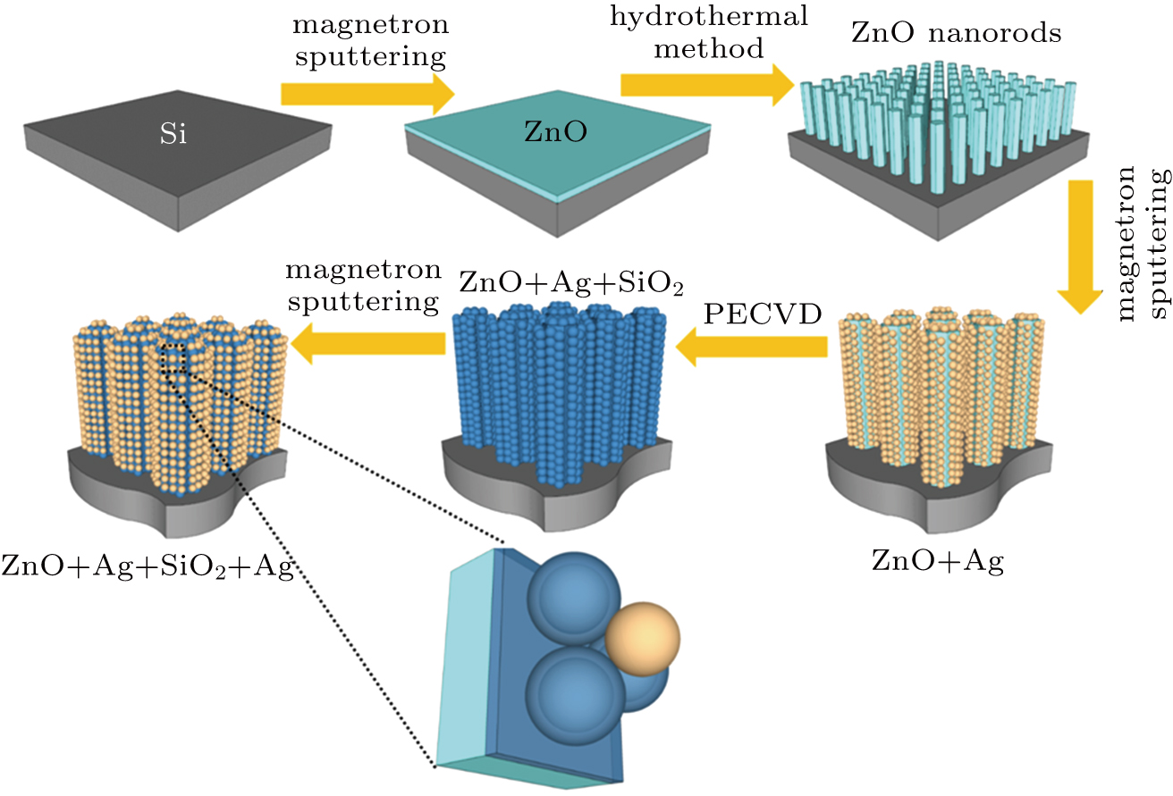
The fabrication process of multilayer SERS substrate is illustrated schematically in Fig. 1. After ultrasonically cleaning the ITO conductive glass substrates with acetone, ethanol, and deionized water, zinc oxide seed layers were deposited on ITO conductive glass substrates by magnetron sputtering. For the growth of ZnO nanorods, hydrothermal growth process was followed, where the precursor solution was prepared with Zn(NO3)2 · 6H2O solution and C6H12N4 solution with equal molar concentration (0.25 M). Then the mixture of precursor solutions was added to a 30-ml Teflon-lined stainless steel autoclave, and the substrates were vertically placed in the autoclave. The autoclave was kept in a hot air oven at 90 °C for 4 h. After the hydrothermal reaction, the substrates were removed and rinsed with deionized water and methanol followed by drying at 100 °C. Then, a 10-nm-thick Ag film was deposited on the ZnO nanorod arrays by magnetron sputtering for 67 s. Further, ultrathin SiO2 film of 2 nm in thickness was deposited on the ZnO@Ag nanorods arrays by the PECVD technology. Finally, the Ag NPs with different thickness values such as 10 nm, 30 nm, 50 nm, and 70 nm, respectively were decorated on ZnO@Ag/SiO2 nanorod arrays by magnetron sputtering technique.

Fig. 1. Schematic diagram of fabrication process of multilayer SERS substrate.
2.2. Characterizations

The 3D SERS substrates were analyzed by scanning electron microscopy (SEM) (FEI/Nova Nano SEM 450). The SERS measurements were performed at room temperature with a Raman microscope (Horiba Jobin Yvon/LabRAM HR Evolution). The wavelength of the excitation laser of SERS experiments was 532 nm, the laser power was about 1 mW, the spectra acquisition time was 10 s, and an optical microscope with a 100× objective lens was used. The laser beam was normally incident on the substrate, which was parallel to the surface normal for SERS spectra collection. In this study, the plasma enhanced chemical vapor deposition system (SENTECH/SI 500D) was used to grow SiO2 dielectric layer, and the multi-cathode sputter deposition platform (Denton Vacuum/Discovery 635) was used to implement the metal deposition. Rhodamine 6G (R6G) was used as the probe molecule for the SERS test. The solution was diluted to a solution with a concentration of 1 × 10⁻⁶ M. The prepared ZnO@Ag/SiO2@Ag substrate was soaked for 12 h and then washed with ethanol to obtain the sample to be measured.

3. Results and discussion

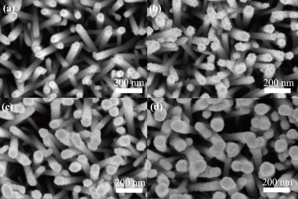
Figure 2 shows the SEM micrographs of the fabricated ZnO nanorods coated with Ag/SiO2@Ag. With the increase of the sputtering time, Ag nanoparticles with a slightly larger size are formed on the surface of the ZnO nanorods. Firstly, with a short magnetron sputtering duration of 67 s, a few small Ag nanoparticles of about 10 nm in diameter are sputtered on the surface of ZnO as the inner layer Ag nanoparticles. Secondly, with a short deposition duration of 8 s, a 2-nm ultrathin uniform SiO2 layer is deposited on the surfaces of Ag nanoparticles. For a sputtering duration of 67 s, the size of Ag nanoparticles is about 10 nm. For a longer magnetron sputtering duration of 470 s, the size of outer layer Ag nanoparticles become larger, about 70 nm.

Fig. 2. (a) and (b) SEM micrographs of the fabricated ZnO nanorods coated with Ag/SiO2@Ag for (a) outer layer Ag nanoparticles sputtering duration of 67 s and Ag nanoparticle size of about 10 nm, (b) outer layer Ag nanoparticles sputtering duration of 200 s and Ag nanoparticle size of about 30 nm, (c) outer layer Ag nanoparticle sputtering duration of 334 s and Ag nanoparticle size of about 50 nm, and (d) outer layer Ag nanoparticle sputtering duration of 470 s and Ag nanoparticle size of about 70 nm.

The ZnO@Ag/SiO2 nanorods are further investigated by using transmission electron microscope (TEM) and energy dispersive x-ray spectroscopy (EDXS) as shown in Fig. 3. Figure 3(a) intuitively shows that the deposited Ag/SiO2 film is distributed uniformly on the ZnO nanorods. The estimated diameter of ZnO nanorods is about 40 nm on average. Figure 3(b) shows a highly magnified TEM image of ZnO@Ag/SiO2 nanorod. It is recognized that the 2-nm SiO2 dielectric layer covers the surfaces of Ag nanoparticles inside the 10-nm-thick inner layer. Figure 3(c) shows the side view of the ZnO nanorods coated with 10-nm Ag and 2-nm SiO2. The average height of ZnO nanorods is about 1 μm. In order to further visualize the distributions of SiO2 and Ag, EDXS elemental mapping of the ZnO@Ag/SiO2 nanorods is introduced to reveal the distributions of elements Zn, Ag, Si, and O as shown in Figs. 3(d)3(h). Meanwhile, the reasons for using ZnO nanorods as 3D supporting substrate are twofold: firstly, ZnO 3D nanostructure is easier to prepare than others, secondly, there is electron-transfer between ZnO and Ag, and the ZnO semiconductor material facilitates the SERS enhancement due to the chemical enhancement effect which has been demonstrated as one of the suitable materials for SERS.[21]

Fig. 3. (a) TEM image of an individual ZnO@Ag/SiO2 nanorod with 67-s inner layer Ag sputtering time and 8-s SiO2 PECVD growth time. (b) Magnified TEM image showing 2-nm-thick SiO2 dielectric layer. (c) The side view SEM micrograph of ZnO nanorods coated with 10-nm-thick Ag layer and 2-nm-thick SiO2 layer. (d)–(h) Dark-field scanning TEM and EDXS elemental mapping.

As is well known, the SERS performance of multilayer structure is mainly determined by the density and morphologies of outer layer noble metal nanoparticles. In order to evaluate the importance of the outer layer noble metals, the SERS spectra of the as-prepared samples are systematically collected. Figure 4 shows the SERS spectra obtained from different-thickness Ag layer-coated 3D multilayer composite structure substrate with a layer of R6G molecules, and typical characteristic Raman peaks of R6G in a range of 500 cm−1–2000 cm−1. Specifically, the Raman spectrum of R6G molecules has strong characteristic vibration peaks at 1185 cm−1, 1315 cm−1, 1366 cm−1, and 1516 cm−1, resulting from the C–H in-plane bending mode, C–O–C stretching mode, and C–C stretching mode. It can be seen in Fig. 4 that the order of the SERS signal intensity is as follows: S4 (for 70-nm-thick Ag layer) > S3 (for 50-nm-thick Ag layer) > S2 (for 30-nm-thick Ag layer) > S1 (for 10 nm-thick Ag layer). It is clearly concluded that the intensity of Raman peak is a function of Ag outer layer thickness, the SERS enhancement intensity from S4 at 1655 cm−1 is about four times stronger than that from S1, the SERS substrate S4 shows the best performance, which may be due to its higher electromagnetic field enhancement. The different SERS response behaviors of multilayer structures may be due to the electron transfer between ZnO and Ag and different electromagnetic enhancement of Ag NPs with different thicknesses and adsorption molecular concentrations. Firstly, the 3D ZnO@Ag/SiO2@Ag multilayer structure has a large surface area, leading R6G molecules to increase. Secondly, due to the fact that the Fermi energy level of ZnO (5.2 eV) is lower than that of Ag (4.26 eV), the electron transfer from Ag-NPs to ZnO will cause the charges to be redistributed, there exists a highest charge-density region in the adjacent face of Ag-NPs and ZnO. The charge redistribution between ZnO and Ag will increase the adjacent face charge density of ZnO and Ag nanoparticles, and thus causes localized electromagnetic field to increase, thereby improving the SERS signals. Finally, the outer-layer Ag nanoparticle size is conducive to the improvement of the SERS performance. The average enhancement factor (EF) can be calculated according to the standard equation: EF = (ISERS/IRaman)/(Nsurface/Nbulk),[28] where ISERS denotes the intensity of the vibrational mode measured on ZnO@Ag/SiO2@Ag substrate and IRaman represents the normal Raman intensity of the same vibrational mode measured on bulk R6G molecules. Nbulk and Nsurface are the numbers of absorbed R6G molecules illuminated by the laser focus spot under normal Raman and SERS conditions respectively. The vibration peak at 617 cm−1 is selected for calculating the EF. The EF of S4 can be estimated to be on the order of 3.05 × 10⁷. Obviously, we present the data demonstrating that the ZnO@Ag/SiO2@Ag multilayer nanorod arrays exhibit the better SERS performance.

Fig. 4. (a) Surface-enhanced Raman scattering spectra of R6G molecules adsorbed on ZnO@Ag/SiO2@Ag nanorods with different-thickness outer-layer Ag (S1: sputtering time 67 s, S2: sputtering time 200 s, S3: sputtering time 334 s, S4: sputtering time 470 s), (b) SERS spectra of R6G molecules adsorbed on ZnO@Ag/SiO2@Ag nanorods with different-thickness Ag and dielectric layer SiO2 with keeping inner layer 10-nm Ag constant (G1: 5-nm-thick SiO2 layer + sputtering time 67-s out-layer Ag, G2: 2-nm-thick SiO2 layer + sputtering time 67-s out-layer Ag, G3: 5-nm-thick SiO2 layer + sputtering time 334-s out-layer Ag, G4: 2-nm-thick SiO2 layer + sputtering time 334-s out-layer Ag).

In order to confirm the direct influence of SiO2 dielectric layer thickness on SERS performance, the SiO2 dielectric layer is varied with a certain thickness of Ag. Figure 4(b) shows the SERS spectra obtained from different-thickness dielectric layer. The SERS results reveal that the SERS intensity is increased exponentially by 2-nm-thick SiO2 dielectric layer compared with the 5-nm-thick SiO2 dielectric layer, with the Ag inter layer thickness fixed at 10 nm. This was demonstrated in other studies, showing that the ultrathin SiO2 dielectric shell can be attributed to the SERS, that a thicker dielectric layer (SiO2, Al2O3) may reduce the Raman signal strength, and that the dielectric layer should be less than 5 nm in thickness in order to ensure strong electromagnetic field enhancement.[13,29] Because ultrathin SiO2 dielectric shell can isolate the Ag nanoparticles to produce increased SPR and realize electromagnetic field enhancement, Raman signals can be remarkably enhanced. Obviously, the SERS signal intensity is related to the interior silica layer thickness, a relatively thick interior silica layer should weaken the SERS signals. A comparison of the Raman spectra shows that the as-prepared arrays of the ZnO nanorods decorated with Ag/SiO2@Ag having an inner layer Ag nanoparticles under a sputtering duration of 67 s, dielectric layer SiO2 with 2 nm in thickness and an outer layer Ag nanoparticles under a sputtering duration of 470 s have the strongest SERS activity. Theoretical calculation and experimental result show that the ultrathin SiO2 dielectric shell and multilayer structures induce hot spots that provide a giant electromagnetic SERS enhancement.

To better understand the contribution of Ag nanoparticles and dielectric layer in ZnO@Ag/SiO2@Ag multilayer nanorods, a 3D finite difference time domain (FDTD) method is used. Our theoretical results show that there are stronger electromagnetic enhancements on the interface between Ag nanoparticles and dielectric layer, and that the resonant coupling between the inner dielectric layer core and outer Ag layer can propagate surface plasmons to induce SPR with enhanced electrical fields as shown in Fig. 5. This is consistent with the experimental result. In comparison with the conventional SERS substrate, on the one hand, the 3D substrate can generate large-area hot spots and achieve high field enhancement factor simultaneously. On the other hand, by comparing with other 3D substrates, the ZnO as semiconductor supporting the chemical enhancement effect has great potential as SERS substrate.

Fig. 5. Calculated electric field intensity distributions of ZnO@Ag/SiO2@Ag multilayer nanorods with different-thickness out-layer Ag at a wavelength of 532 nm in xz plane, with (a) sputtering time being 67 s and size of Ag nanoparticles about 10 nm, (b) sputtering time being 200 s and size of Ag nanoparticles about 30 nm, and (c) sputtering time 334 s and size of Ag nanoparticles about 50 nm, (d) sputtering time being 470 s and size of Ag nanoparticles about 70 nm.
4. Conclusions

In this work, ZnO@Ag/SiO2@Ag multilayer structure is successfully synthesized by the physico–chemical combination method. The geometries of the nanorods and the thickness of dielectric layer and Ag layer can be well controlled, which opens up the way to modulating the local electric field and therefore the SERS enhancement factor is controlled. The products are characterized by SEM, TEM, Raman spectrum, and theoretical simulation. By regulating the thickness of both the Ag outer-layer and the SiO2 dielectric layer, the ultimately optimized SERS substrate is implemented. The experimental results accord with FDTD simulation. Our results suggest that the ZnO@Ag/SiO2@Ag substrate is feasible to generate large-area hot spots and achieve high field enhancement factor simultaneously. Moreover, comparing with the ZnO@Ag or Ag@SiO2@Ag structures, the proposed method can achieve 3D multilayer structure electromagnetic field regulation, and the simplicity and generality of our method for further understanding the SERS mechanism induced by the SPR effect offer great advantages. In view of the green and sustainable application protocol, we expect that the 3D multilayer structure has potential applications in flexible substrate, SERS, photocatalysis and biological imaging.

Reference
[1] Shanmukh S Jones L Driskell J Zhao Y Dluhy R Tripp R A 2006 Nano Lett. 6 2630
[2] Kneipp K Kneipp H 2006 Accounts. Chem. Res. 39 443
[3] Deng X G Brartiun G B Liu S Sciortino P F Koefer B Tombler T Moskovits M 2010 Nano Lett. 10 1780
[4] Fang Z Cai J Yan Z Nordlander P Halas N J Zhu X 2011 Nano Lett. 11 4475
[5] Tong L M Xu H X 2012 Physics 41 582 in Chinese
[6] Atwater H A Polman A 2010 Nat. Mater. 9 205
[7] Brolo A G 2012 Nat Photon. 6 709
[8] Zhao J Sun M T Liu Z Quan B G Gu C Z Li J J 2015 Sci. Rep. 5 16019
[9] Naik G V Shalaev V M Boltasseva A 2013 Adv. Mater. 25 3264
[10] Comin A Manna L 2014 Chem. Soc. Rev. 43 3957
[11] Liu L W Zhou W Q Zeng Z Q Jin M L 2016 J. Raman Spectrosc. 47 1200
[12] Zhang Y J Sun H H Gao R X Zhang F Zhu A Chen L 2018 Sens. & Actuators B: Chemical 272 34
[13] Chen C Zhou X Ding T T Zhang J Wang S Xu J Chen J W Dai J N Chen C Q 2016 Mater. Lett. 165 55
[14] Zhou J Zhang J S Xian G Qi Q Gu S Z Shen C M Cheng S H He S T Yang H T 2019 Chin. Phys. 28 083301
[15] Huang T Cao L Zhang X Xiong X Y Xu J J Xiao R S 2019 J. Alloys Compd. 790 127
[16] Wu C L Hsueh C H Li J H 2019 Opt. Express 27 1660
[17] Liu Y J Xu C X Zhu Z You D T Wang R Qin F F Wang X X Cui Q N Shi Z L 2018 Cryst. Growth & Design 18 5279
[18] Pal A K Pagal S Prashanth K Chandra G K Umapathy S Mohan D B 2019 Sens. & Actuators B: Chemical 279 157
[19] Yang J L Li R P Han J H Huang M J 2016 Chin. Phys. 25 083301
[20] Tian Y Wang H F Yan L Q Zhang X F Attia F Chen P P Dong F L Sun L F Chu W G 2018 Chin. Phys. 27 077406
[21] Lei S J Tao C J Li J L Zhao X Wang W Z 2018 Appl. Surf. Sci. 452 148
[22] Li J F Anema J R Wandlowski T Tian Z Q 2015 Chem. Soc. Rev. 44 8399
[23] Tang H B Meng G W Huang Q Zhang Z Huang Z L Zhu C H 2012 Adv. Funct. Mater. 22 218
[24] Zhao Y Zeng W C Tao Z C Xiong P H Qu Y Zhu Y W 2015 Chem. Commun. 51 866
[25] Huang J A Zhao Y Q Zhang X J He L F Wong T L Chui Y S Zhang W J Lee S T 2013 Nano Lett. 13 5039
[26] Hu Z S Liu Z Li L Quan B G Li Y J Li J Gu C Z 2014 Small 10 3933
[27] Xu L L Li S Li F Zhang H Wang D M Chen M Chen F 2017 Opt. Mater. Express 7 3137
[28] Liu K Bai Y Zhang L Yang Z Fan Q Zheng H Yin Y Gao C 2016 Nano Lett. 16 3675
[29] Ma L W Huang Y Hou M J Li J H Xie Z Zhang Z J 2016 J. Phys. Chem. 120 606