Selective synthesis of three-dimensional ZnO@Ag/SiO2@Ag nanorod arrays as surface-enhanced Raman scattering substrates with tunable interior dielectric layer
Project supported by the Fund from the Science and Technology Department of Jilin Province, China (Grant No. 20170520108JH), the Beihua University Youth Nurtural Fund, China (Grant No. 2017QNJJL15), the Beihua University PhD Research Start-up Fund, China (Grant No. 202116140), and the Undergraduate Innovation Project, China (Grant No. 220718100).
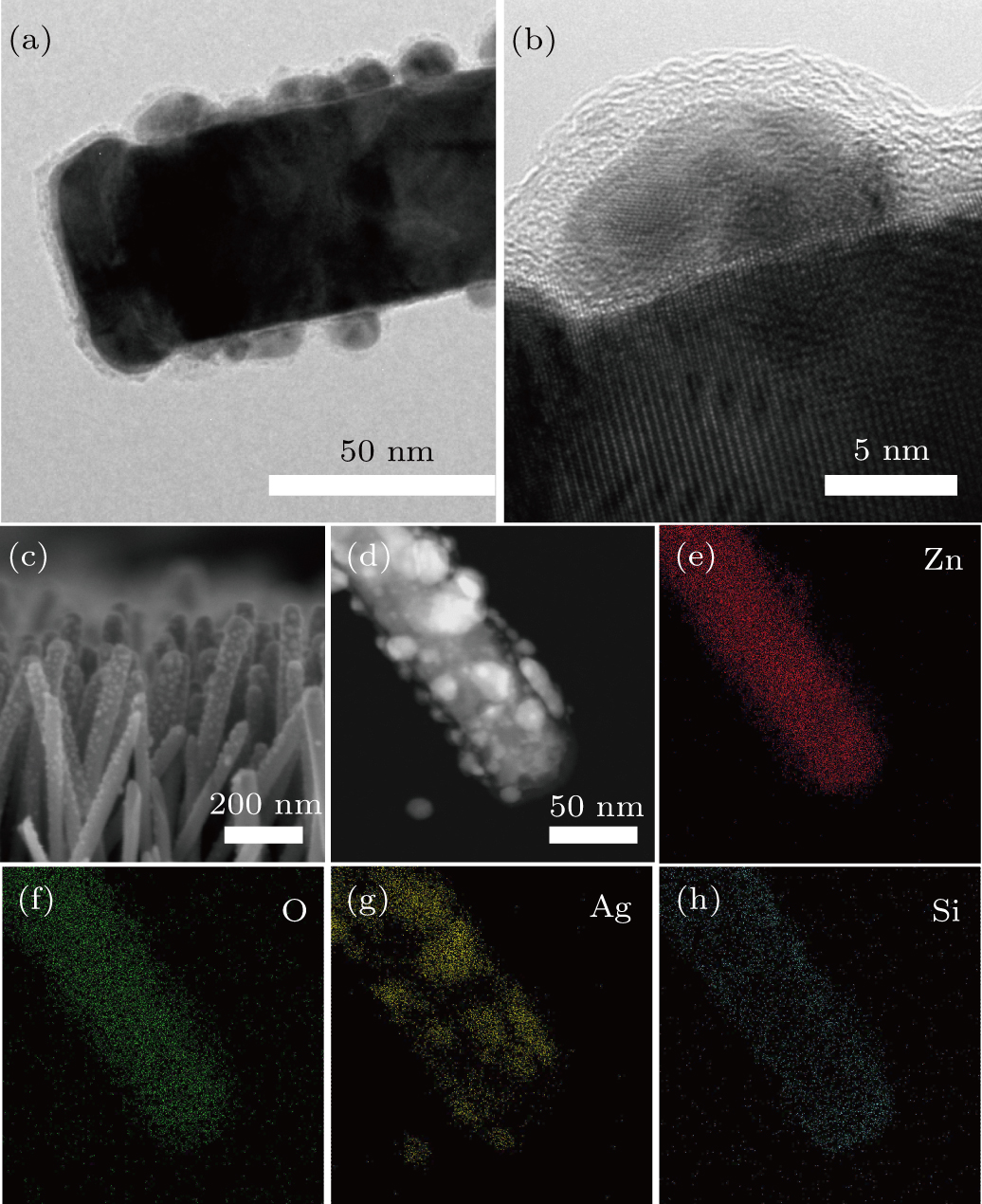
(a) TEM image of an individual ZnO@Ag/SiO2 nanorod with 67-s inner layer Ag sputtering time and 8-s SiO2 PECVD growth time. (b) Magnified TEM image showing 2-nm-thick SiO2 dielectric layer. (c) The side view SEM micrograph of ZnO nanorods coated with 10-nm-thick Ag layer and 2-nm-thick SiO2 layer. (d)–(h) Dark-field scanning TEM and EDXS elemental mapping.
