† Corresponding author. E-mail:
Based on the thermal network of the two-dimensional heterojunction bipolar transistors (HBTs) array, the thermal resistance matrix is presented, including the self-heating thermal resistance and thermal coupling resistance to describe the self-heating and thermal coupling effects, respectively. For HBT cells along the emitter length direction, the thermal coupling resistance is far smaller than the self-heating thermal resistance, and the peak junction temperature is mainly determined by the self-heating thermal resistance. However, the thermal coupling resistance is in the same order with the self-heating thermal resistance for HBT cells along the emitter width direction. Furthermore, the dependence of the thermal resistance matrix on cell spacing along the emitter length direction and cell spacing along the emitter width direction is also investigated, respectively. It is shown that the moderate increase of cell spacings along the emitter length direction and the emitter width direction could effectively lower the self-heating thermal resistance and thermal coupling resistance, and hence the peak junction temperature is decreased, which sheds light on adopting a two-dimensional non-uniform cell spacing layout to improve the uneven temperature distribution. By taking a 2 × 6 HBTs array for example, a two-dimensional non-uniform cell spacing layout is designed, which can effectively lower the peak junction temperature and reduce the non-uniformity of the dissipated power. For the HBTs array with optimized layout, the high power-handling capability and thermal dissipation capability are kept when the bias voltage increases.
In recent years, heterojunction bipolar transistors (HBTs) array with parallel HBT cells layout has been used widely for microwave power applications[1–4] due to its high current handling capability.[5–7] However, the self-heating effect caused by the power dissipation of each HBT cell and the thermal coupling effect among the adjacent HBT cells result in an uneven temperature profile in the HBTs array. Because of the positive temperature coefficient of the emitter current, the central HBT cells with higher temperature will conduct more current and consequently generate more heat, which aggravates the thermal effects and leads to thermal breakdown or thermal runaway.[8,9]
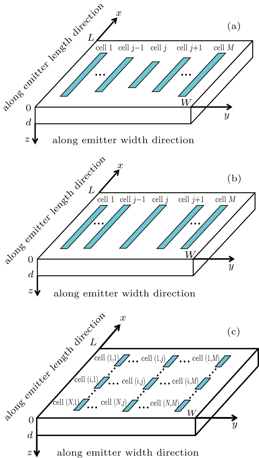
In order to obtain more uniform temperature distribution and tackle these thermal issues, one-dimensional (along emitter width direction) layout design technologies including variation of emitter length in HBT cells[10,11] (in Fig.
It is known that the thermal resistance matrix ([Rij]) could be used to represent the thermal effects of a one-dimensional HBT array,[18,19] which is helpful to design the layout of the device. However, the prior [Rij] representation is not applicable for the 2-D HBTs array.
In this paper, with the aid of the thermal network of a 2-D HBTs array, a new thermal resistance matrix ([Rijkl]) is proposed, including self-heating thermal resistance (Rijij) in the (i, j) HBT cell and thermal coupling resistance (

To account for the self-heating and the thermal coupling effects, a thermal network of 2-D HBTs array (N × M HBT cells) with a ground-referenced thermal voltage is shown in Fig.
 | Fig. 2. Thermal network of a two-dimensional HBTs array with N × M HBT cells by taking into account the self-heating and thermal coupling effects. |
For the (i, j) HBT cell in the thermal network, the self-heating effect can be represented as a parallel combination of Rijij and dissipated power (Pij). The self-heating temperature rise of the (i, j) HBT cell (


 |


Therefore, the peak junction temperature of the (i, j) HBT cell (Tij) including the self-heating temperature rise and the total thermal coupling temperature rise is obtained as
 |
 |


 |
 |


As a result, the thermal-electrical model is established based on the iterative solution between ANSYS and MATLAB, and the temperature of the HBTs array (with N × M HBT cells) is first calculated under the same power level. By increasing the power of the (k, l) HBT cell (


 |
Take a 2 × 1 HBTs array for example, [Rijkl] is calculated, and the impact of cell spacing along the emitter length direction (Sx) on the thermal characteristics of the HBTs array is studied. The layout of the 2 × 1 HBTs array is shown in Fig. 


The impact of Sx on Rijij and 


 | Fig. 4. The self-heating thermal resistance versus cell spacing along emitter length direction in the 2 × 1 HBTs array. |
 | Fig. 5. The thermal coupling resistance versus cell spacing along emitter length direction in the 2 × 1 HBTs array. |
The impact of Sx on the peak junction temperature (Tij) at IC of 0.4 mA and VCE of 5 V is shown in Fig. 
Take a 1 × 2 HBTs array for example, [Rijkl] is calculated, and the impact of cell spacing along the emitter width direction (Sy) on the thermal characteristics of the HBTs array is studied. The layout of the 1 × 2 HBTs array is shown in Fig.
The impact of Sy on Rijij and 


 | Fig. 8. The self-heating thermal resistance versus cell spacing along emitter width direction in the 1 × 2 HBTs array. |
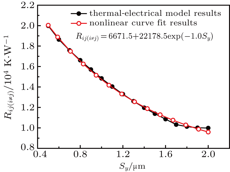 | Fig. 9. The thermal coupling resistance versus cell spacing along emitter width direction in the 1 × 2 HBTs array. |
Figure 


 | Fig. 10. The peak junction temperature versus cell spacing along emitter width direction in the 1 × 2 HBTs array. |
From this analysis, it can be concluded that both Sx and Sy should be designed carefully to effectively decrease Rijij and 

Take a HBTs array with 1 × 20 HBT cells for example, both the simulated temperature profile along the central line across the HBT cells and the measured temperature profile reported in Ref. [15] are shown in Fig.
With the aid of the thermal-electrical model, [Rijkl] of a 2 × 6 HBTs array (array-1) with uniform cell spacings of 

 |
The detail profile of [Rijkl] in array-1 is shown in Fig.
 | Fig. 12. Profile of thermal resistance matrix [Rijkl] (K/W) in the 2 × 6 HBTs array with uniform cell spacing (array-1) at IC of 2.4 mA and VCE of 5 V. |
At the same time, iterations are used to calculate Tij and Pkl of array-1. First, it is assumed that there is an even collector current distribution across all HBT cells. Due to the thermal effects, the temperature of each HBT cell can be calculated with a temperature rise different from the others’. Because of the positive temperature coefficient of 

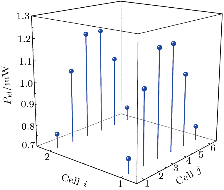 | Fig. 13. The distribution of the dissipated power (Pkl) in the 2 × 6 HBTs array with uniform cell spacing (array-1) at IC of 2.4 mA and VCE of 5 V. |
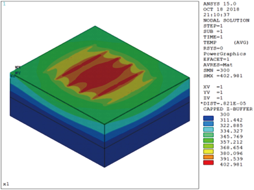 | Fig. 14. Temperature profile of the 2 × 6 HBTs array with uniform cell spacing (array-1) at IC of 2.4 mA and VCE of 5 V. |
In order to improve the uniformity of the Pkl distribution and lower the temperature of the central HBT cells, both of cell spacing along the emitter length direction (Sx) and cell spacing along the emitter width direction (Sy) are designed carefully. For Sx, the spacings between the central cells should be increased significantly to lower Rijij, because 


 |
 |

 | Fig. 15. Layouts of 2 × 6 HBTs arrays (a) with uniform Sx and uniform Sy (array-1), (b) with non-uniform Sx and non-uniform Sy (array-2). |
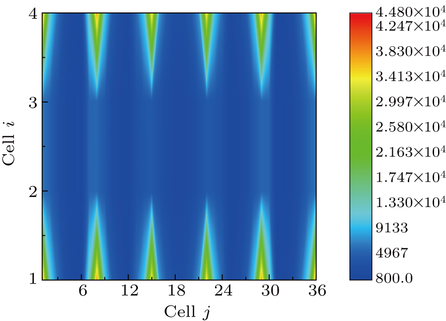 | Fig. 16. Profile of thermal resistance matrix [Rijkl] (K/W) in the 2 × 6 HBTs array with non-uniform Sx and non-uniform Sy (array-2) at IC of 2.4 mA and VCE of 5 V. |
| Table 1.
Cell spacing along emitter length direction of the two types of HBTs arrays. . |
| Table 2.
Cell spacing along emitter width direction of the two types of HBTs arrays. . |
The correlated Pkl and the temperature profile of array-2 are shown in Figs.
 | Fig. 17. The distribution of the dissipated power (Pkl) in the 2 × 6 HBTs array with non-uniform cell spacing (array-2) at IC of 2.4 mA and VCE of 5 V. |
 | Fig. 18. Temperature profile of the 2 × 6 HBTs array with non-uniform cell spacing (array-2) at IC of 2.4 mA and VCE of 5 V. |
As the collector–emitter voltage VCE is increased to 7 V, the calculated correlated Pkl and Tij of the HBT cells in the two arrays are shown in Figs.
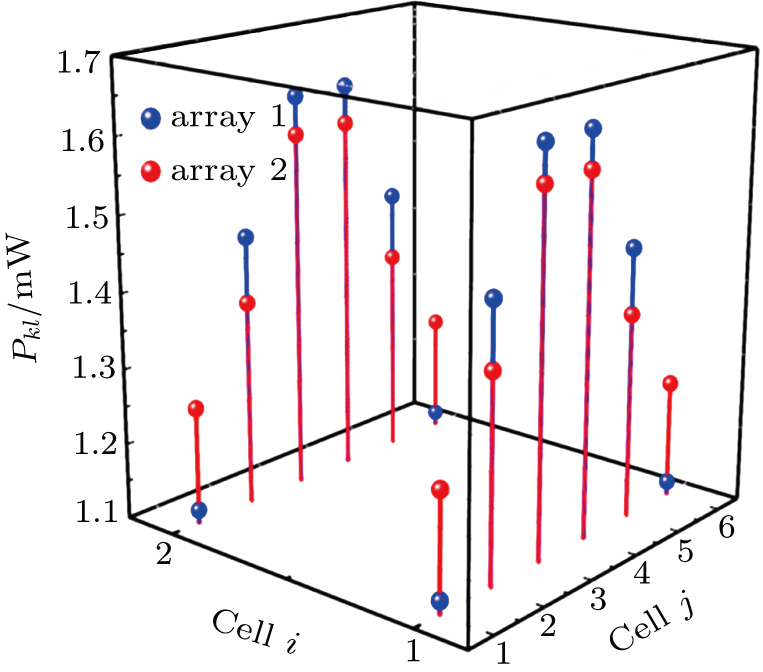 | Fig. 19. Power levels at 
|
To represent the self-heating effect and thermal coupling effect of the HBTs array with N × M HBT cells, [Rijkl] including Rijij and 


| [1] | |
| [2] | |
| [3] | |
| [4] | |
| [5] | |
| [6] | |
| [7] | |
| [8] | |
| [9] | |
| [10] | |
| [11] | |
| [12] | |
| [13] | |
| [14] | |
| [15] | |
| [16] | |
| [17] | |
| [18] | |
| [19] |


