† Corresponding author. E-mail:
Interdigitated back contact silicon hetero-junction (IBC-SHJ) solar cells exhibit excellent performance owing to the IBC and SHJ structures. The front surface field (FSF) layer composed of electric field passivation and chemical passivation has been proved to play an important role in IBC-SHJ solar cells. The electric field passivated layer n+-a-Si: H, an n-type Si alloy with carbon or oxygen in amorphous phase, is simulated in this study to investigate its effect on IBC-SHJ. It is indicated that the n+-a-Si: H layer with wider band gap can reduce the light absorption on the front side efficaciously, which hinders the surface recombination of photo-generated carriers and thus contributes to the improvement of the short circuit current density Jsc. The highly doped n+-a-Si: H can result in the remakable energy band bending, which makes it outstanding in the field passivation, while it makes little contribution to the chemical passivation. It is noteworthy that when the electric field intensity exceeds 1.3 × 10⁵ V/cm, the efficiency decrease caused by the inferior chemical passivation is only 0.16%. In this study, the IBC-SHJ solar cell with a front n+-a-Si: H field passivation layer is simulated, which shows the high efficiency of 26% in spite of the inferior chemical passivation on the front surface.
The interdigitated back contact (IBC) solar cell was first proposed by Lammert and Schwartz in 1975.[1] With the emitter placed at the back, the interdigitated structure is formed, which eliminates the electrode shading and thus can improve the short circuit current density Jsc. Sun Power demonstrated that the efficiency of IBC solar cells reached 25.2% in 2016.[2] Silicon hetero-junction (SHJ) solar cells were pioneered in the early 1990s by Sanyo. Panasonic and Kaneka further increased the conversion efficiency up to 24.7% and 25.1%, respectively.[3,4] The SHJ structure, with a hydrogenated amorphous silicon (i-a-Si: H) layer embedded in the hetero-junction, is adopted to chemically passivate the hetero-interface and can therefore significantly enhance the open circuit voltage Voc.
The IBC-SHJ solar cells, can not only avoid the front optical loss but also take advantage of hetero-junctions, leading to the high efficiency due to the improvement of Jsc and Voc.[5] These properties were sufficiently utilized by Panasonic and Kaneka and they achieved conversion efficiencies up to 25.6% and 26.6%, respectively,[6,7] which get close to the theoretical limit.[8]
The front surface field (FSF) structure, a stack of i-a-Si: H and P heavily doped a-Si (n+-a-Si: H) layers, passivates the surface dangling bonds, and separates the photo-generated electron–hole pairs. As a consequence, the surface recombination can be effectively suppressed. The current density and voltage decrease dramatically since the surface passivation deteriorates.[9,10] In order to achieve the favorable chemical passivation, the i-a-Si: H layer is required to be deposited between c-Si and a-Si: H.[11–13] However, because of the higher absorption coefficient of a-Si: H than that of Si, a-Si: H will significantly reduce the spectrum response, therefore leading to the decrease of Jsc directly.[14,15] Besides, it is reported that each thickness increase by 10 nm can lead to the Jsc decrease by 1.5 mA/cm2.[15] More importantly, the induced widen band gap n+-a-Si: H, as a field passivated layer, is requisite to mitigate the loss of spectrum. Many researches about the front surface light enhance and surface passivation have been carried out.[16–20] The existing researches have been mainly focused on the i-a-Si: H deposition technology and its effects on the interface passivation of IBC-SHJ solar cells,[21] without fully considering the influence of the n+-a-Si: H layer. To overcome this deficiency, the present study attempts to investigate the mechanism by integrating the optical loss and passivation of solar cells. Consequently, in this study, the n+-a-Si: H properties of wider band gap on optical absorption, the effect of the doping concentration on the field passivation, and its combined action with chemical passivation are scrutinized by a two-dimensional simulation tool Sentaurus TCAD. All the parameters used in the modeling are consistent with those in experiments and measurements.
In this work, the solar-grade n-type c-Si wafers with (100) orientation are used in the experiment. The resistivity is 

The n+-a-Si: H(O/C) thin films are deposited on quartz substrates using a gas mixture comprising silane (SiH4), hydrogen (H2), phosphorane (PH3), and methane (CH4) or nitrogen dioxide (NO2) under the pressure of 70 Pa. The plasma power is 10 W, and the substrate temperature is 250 °C.
The effective minority carrier lifetime (τeff) measurements are performed on the samples with i-a-Si:H layers on the front and the back sides of the silicon wafers, respectively, which are realized by using the quasi-steady-state photoconductance (QSSPC) method (WCT-120, Sinton Instruments, USA). The optical properties are tested by a UV-3600 Plus UV–VIS–NIR spectrophotometer. The doping profiles of the doped a-Si thin films are measured by electrochemical capacitance–voltage (ECV) profiling (CVP21, WEP, Germany).
As shown in Fig.
In IBC-SHJ, Jsc and Voc increase dramatically when the front surface chemical passivation ameliorates,[9] which means that the thicker i-a-Si: H is beneficial for the chemical passivation. But thicker i-a-Si: H layer would induce optical loss in the front surface. The 5 nm thick i-a-Si: H is chosen to provide chemical passivation in the simulation.
As shown in Fig. 


The transmission and reflectance spectra of different P doped Si-based alloy materials are tested by the UV-3600 Plus UV–VIS–NIR spectrophotometer. The band gap width of different n+-a-Si: H materials is in effect modulated by altering the a-Si morphology or impurity compound.
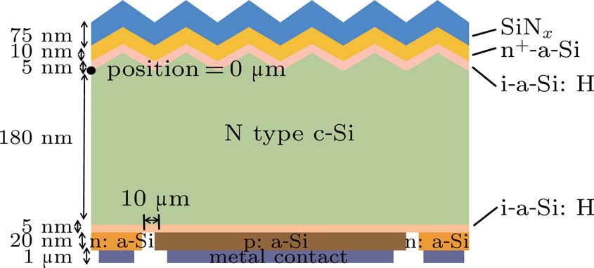
The simulator Sentaurus TCAD is extensively used for modeling solar cells based on the calculation of Possion equation and carrier continuity equation. The unit cell of the IBC-SHJ solar cells studied in this case is shown in Fig. 


| Table 1.
Default parameters used in the simulation. . |
The substrate doping is set to be 2 × 1015 cm−3 to match the wafer’s resistivity. The effective doping concentrations of n+-a-Si: H and p+-a-Si: H are imported according to the ECV measurement results, as shown in Fig.
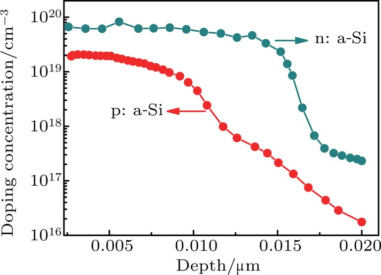 | Fig. 4. Doping concentrations of n+-a-Si: H and p+-a-Si: H thin films on the back of IBC-SHJ solar cells. |
The energy band model is based on the following equation:[24]
The energy band diagram of n+-a-Si: H/i-a-Si: H/c-Si/i-a-Si: H/p+-a-Si: H in thermal equilibrium is shown in Fig.
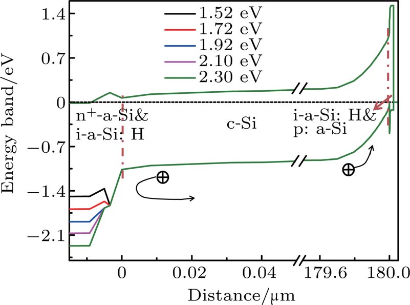 | Fig. 5. Energy band diagram of n+-a-Si: H/i-a-Si: H/c-Si/i-a-Si: H/p+-a-Si: H with different band gaps in thermal equilibrium. |
The reason is that the constant doping concentration of n+-a-Si: H defines the position of the Fermi level. And the bending does not vary with the constant Fermi level position. Thus, the bending at the i-a-Si: H/c-Si interface is not influenced by the band gap of n+-a-Si: H. Although the interface band bending does not change, the band structure on the front surface is still different. Figure
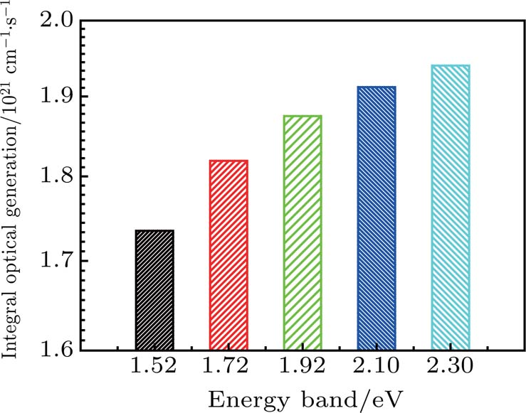 | Fig. 6. Integral photo-generated carriers in the entire substrate section with different band gaps under AM1.5 illumination. |
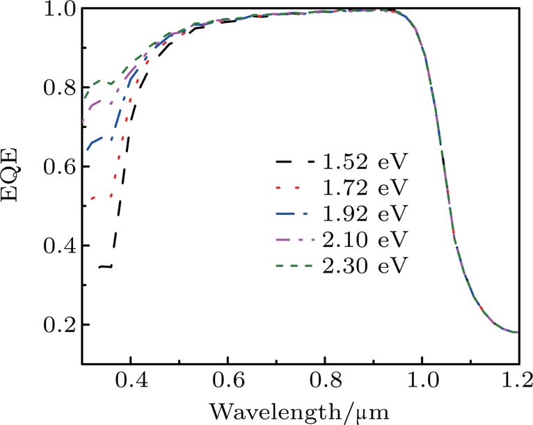
It can be seen from the external quantum efficiency (EQE) curve of the IBC-SHJ solar cells in Fig.
The energy band diagram of n+-a-Si: H/i-a-Si: H/c-Si/i-a-Si: H/p+-a-Si: H with different doping concentration under thermal equilibrium is shown in Fig.
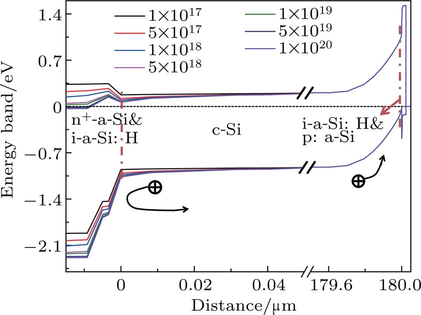 | Fig. 8. Energy band diagram of n+-a-Si: H/i-a-Si: H/c-Si/i-a-Si: H/p+-a-Si: H with different doping concentration (in cm−3) in thermal equilibrium. |
The band bending at the interface can also be attributed to the change of the Fermi level. The higher the doping concentration is, the closer the Fermi level is to the conduction band, as shown by the following equation:

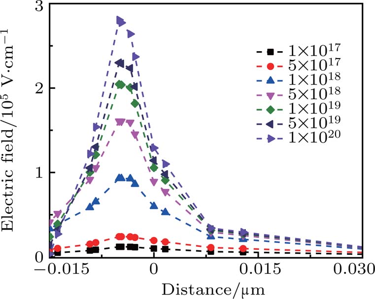
The separation of electron–hole pairs on the front surface is due to the selection of the electric field. As shown in Fig.
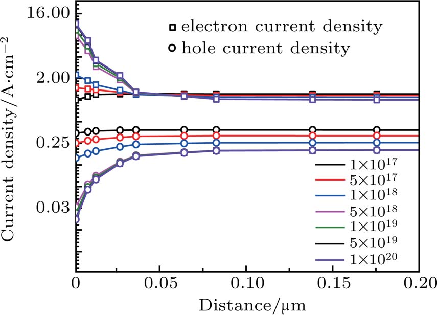 | Fig. 10. Electron and hole current densities near IBC-SHJ front surface with different doping concentrations (in cm−3). |
Figure
The mutual action between chemical and field passivations on the front surface is also considered. As shown in Fig. 
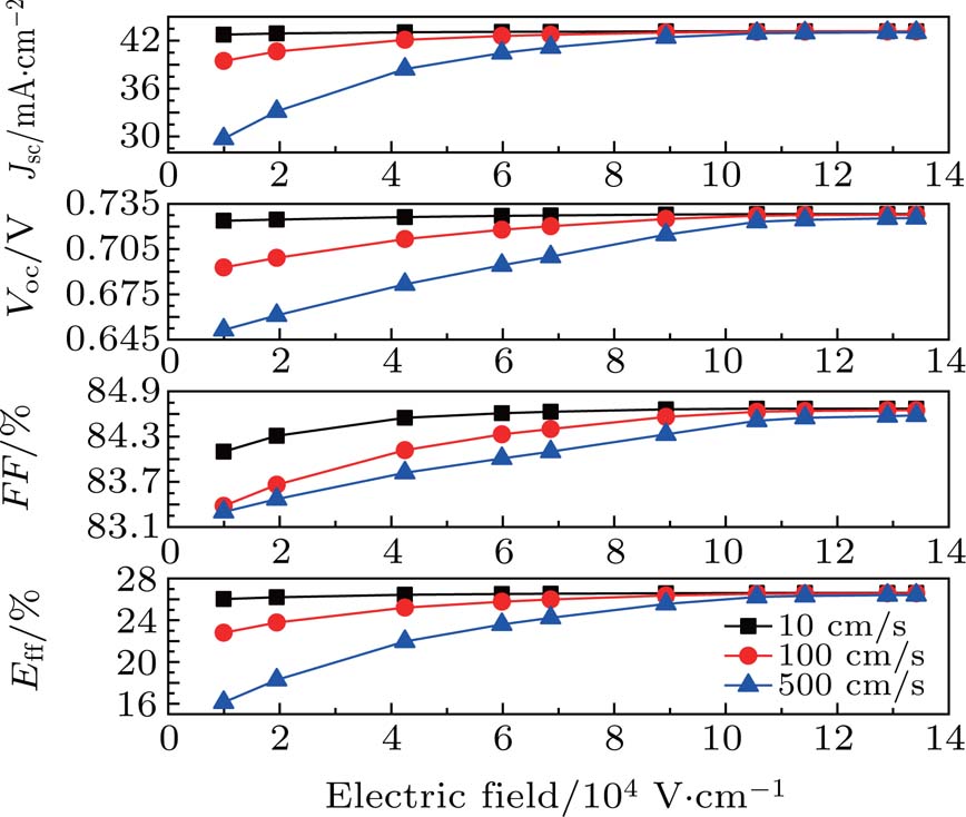 | Fig. 11. The Jsc, Voc, FF, and Eff due to the total effect of chemical passivation and electric field passivation. |
It can be seen that with the same chemical passivation, the Jsc, Voc, FF, and Eff increase with the increasing electric field on the front surface. Eff decreases from 26.57% to 22.81% when the electric field reduces from 1.3 × 10⁵ V/cm to 1 × 10⁴ V/cm when S is 100 cm/s. And Eff decreases from 26.41% to 16.13% when the electric field reduces from 1.3 × 10⁵ V/cm to 1 × 10⁴ V/cm with S of 500 cm/s. Under the condition of the same electric field passivation, the Jsc, Voc, FF, and Eff decay with the worsening chemical passivation. When the electric field passivation is strong (
The S of 100 cm/s represents the poor chemical passivation condition (5 nm i-a-Si: H layer). The optical and electrical properties of n+-a-Si thin films are compared comprehensively. Figure
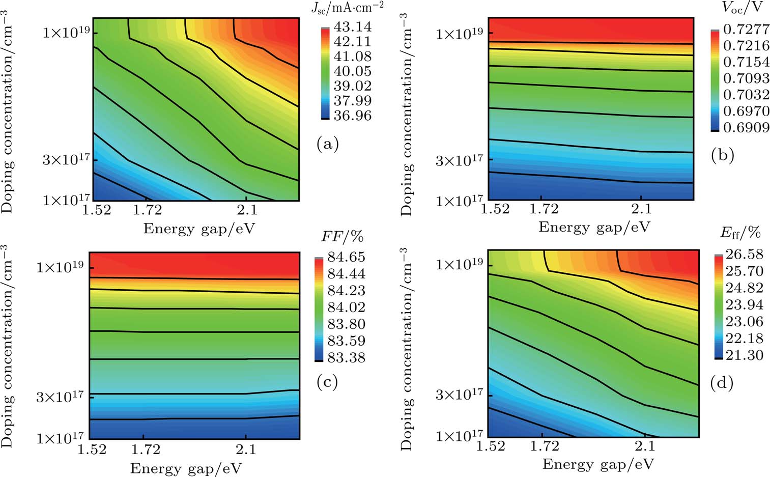 | Fig. 12. The (a) Jsc, (b) Voc, (c) FF, and (d) Eff of IBC-SHJ solar cells with different doping concentrations and band gaps. |
It is manifested that Jsc enhances with the increasing band gap width and doping concentration. The broadening of the band gap can reduce the light absorption by amorphous silicon and increase the absorption in the substrate. The high doping concentration can enhance the field passivation of the cell, and thus significantly improve the Voc. The FF increases with the increase of the doping concentration as the recombination is suppressed. The combined effect of these two factors enables the IBC-SHJ to achieve a conversion efficiency of over 26% in spite of the poor chemical passivation.
In the present study, the n+-a-Si: H materials with different band gaps and doping concentrations are applied to the FSF of IBC-SHJ solar cells, and investigated by Sentaurus TCAD tools. The results show that the light absorption of the stack of amorphous silicon films decreases with the widening band gap, which generates more photo-generated carriers and improves the external quantum efficiency of the solar cells. However, the wide band gaps do not contribute to the band bending at the i-a-Si: H/c-Si interface, and thus have no effect on the front field passivation. And the bending is mainly affected by the doping concentration. With the increasing doping concentration, the energy band is more seriously bending, which means a higher potential barrier for holes.
According to the distribution of the electric field and carrier current density on the front surface, it is shown that the electric field becomes stronger, and enhances the selectivity of electrons while restrains the transportation of minority carriers, and the recombination of two carriers is reduced. In addition, the relationship between the field passivation and the chemical passivation is also investigated. When the chemical passivation is constant, Jsc, Voc, FF, and Eff of IBC-SHJ increase with the enhancement of the field passivation. When the field passivation is strong enough (
| [1] | |
| [2] | |
| [3] | |
| [4] | |
| [5] | |
| [6] | |
| [7] | |
| [8] | |
| [9] | |
| [10] | |
| [11] | |
| [12] | |
| [13] | |
| [14] | |
| [15] | |
| [16] | |
| [17] | |
| [18] | |
| [19] | |
| [20] | |
| [21] | |
| [22] | |
| [23] | |
| [24] |


