Improving robustness of GGNMOS with P-base layer for electrostatic discharge protection in 0.5- μ m BCD process
Hou Fei1, Chen Ruibo2, Du Feibo1, Liu Jizhi1, Liu Zhiwei1, †, J Liou Juin2
State Key Laboratory of Electronic Thin Films and Integrated Devices, University of Electronic Science and Technology of China, Chengdu 610054, China
School of Information Engineering, Zhengzhou University, Zhengzhou 450001, China


† Corresponding author. E-mail: ziv_liu@hotmail.com

Abstract

Gate-grounded N-channel MOSFET (GGNMOS) has been extensively used for on-chip electrostatic discharge (ESD) protection. However, the ESD performance of the conventional GGNMOS is significantly degraded by the current crowding effect. In this paper, an enhanced GGNMOS with P-base layer (PB-NMOS) are proposed to improve the ESD robustness in BCD process without the increase in layout area or additional layer. TCAD simulations are carried out to explain the underlying mechanisms of that utilizing the P-base layer can effectively restrain the current crowing effect in proposed devices. All devices are fabricated in a 0.5- BCD process and measured using the transmission line pulsing (TLP) tester. Compared with the conventional GGNMOS, the proposed PB-NMOS devices offer a higher failure current than its conventional counterpart, which can be increased by 15.38%. Furthermore, the PB-NMOS_type3 possesses a considerably lower trigger voltage than the conventional GGNMOS to protect core circuit effectively.

PACS: 85.30.De
1. Introduction

Gate-grounded N-channel MOS (GGNMOS) is widely used in electrostatic discharge (ESD) protection because of its active discharge mechanism and compatibility of bipolar-CMOS–DMOS (BCD) technologies.[1] However, as the technology advances, design of area efficient and robustness GGNMOS becomes extremely challenging, due to the lightly doped drain (LDD) existing in deep-submicron BCD technology aimed at overcoming the hot-carrier effect, which leads to significant current crowding and consequently degradation of GGNMOS device’s ESD robustness.[2] Several studies have been reported to improve the ESD robustness of GGNMOS, including the incorporation of substrate-triggering,[3] gate-coupled technologies,[4] drain/source silicide blocking,[5,6] and P-ESD implantation.[79] Among them, the approaches of substrate-triggering and gate-coupled technologies are realized by introducing additional resistors for triggering-assist, which will consume more layout area and cost. Likewise, the approach of drain/source silicide blocking will increase drain contact-to-gate space (DCGS) and source contact-to-gate space (SCGS), which will also consume more layout area and cost. Unlike, the approach of adding the P-ESD implantation layer in the GGNMOS is attractive as it can introduce an extra vertical current path during the ESD event,[79] without increasing layout area. Nevertheless, this method will induce a sharp increase in leakage current.[10] Furthermore, ESD implantation is not a standard step in BCD process, thus resulting in an increase in fabrication cost and complexity.

To improve the ESD characteristics without increase in layout area and fabrication cost, an enhanced GGNMOS by using P-base layer (PB-NMOS) are proposed in this work. As the base region of bipolar transistor, P-base layer is an inherent layer in BCD process.[11] And thus, no extra step and/or cost will incur in proposed PB-NMOS. Three types of PB-NMOS will be designed and fabricated in 0.5- BCD process.

2. Proposed device structures and simulations

The cross-sectional view of conventional GGNMOS is shown in Fig. 1(a). The cross-sectional views of proposed three types of PB-NMOS are shown in Figs. 1(b), 1(c), and 1(d), respectively. PB-NMOS_type1 introduces P-base layer underneath the drain of NMOS and the length of P-base (LPB) is smaller than the length of drain (LD). Unlike the PB-NMOS_type1, LPB of PB-NMOS_type2 is equal to LD. PB-NMOS_type3 incorporates P-base layer surrounding the entire active area.
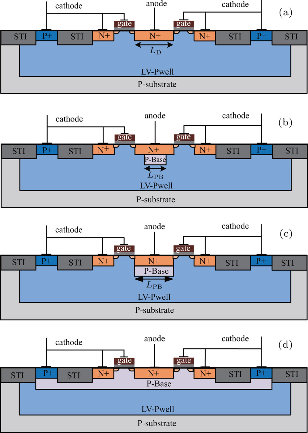
Fig. 1. Cross-sectional views of (a) conventional GGNMOS, (b) proposed PB-NMOS_type1, (c) proposed PB-NMOS_type2, and (d) proposed PB-NMOS_type3.

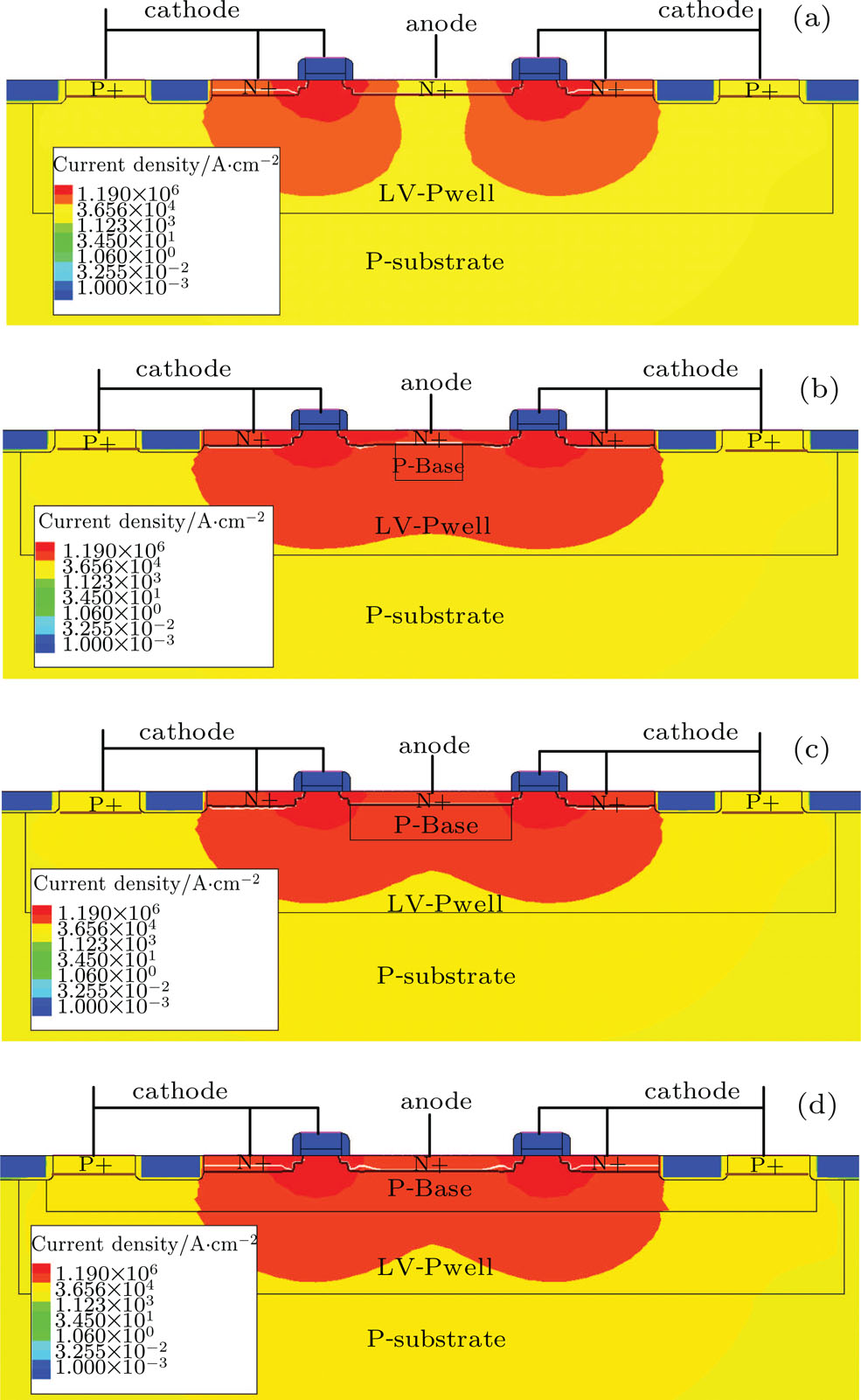
In order to further explore the physics mechanisms of the GGNMOS and proposed PB-NMOS, two-dimensional (2D) Technology Computer-Aided Design (TCAD) simulation has been carried out by Sentaurus tool,and all the layers and dimensions are set according to the design rules of a real 0.5- BCD process. Figure 2 shows the simulation results of three devices under the post-trigger mode at a current of 1 mA/ m. The current density distribution of the conventional GGNMOS is shown in Fig. 2(a). It is clear that ESD current is discharged mainly through the shallow LDD region of the NMOS device, making it valuable to ESD-induced self-heating effect.

Fig. 2. TCAD simulation results of the current density distributions in (a) conventional GGNMOS, (b) proposed PB-NMOS_type1, (c) proposed PB-NMOS_type2, and (d) proposed PB-NMOS_type3.

However, the current crowding effect is effectively alleviated in proposed PB-NMOS_type1 due to the imbedded P-base layer which induces an additional vertical NPN current path, as shown in Fig. 2(b). Figure 2(c) illustrates that the current density distribution of proposed PB-NMOS_type2 is more uniform than that of proposed PB-NMOS_type1, which will enhance the ESD robustness of proposed PB-NMOS_type2. Similar to the PB-NMOS_type1 and PB-NMOS_type2, the ESD current in proposed PB-NMOS_type3 also branches out to the additional vertical NPN path, as shown in Fig. 2(d), which leads to an increased failure current.

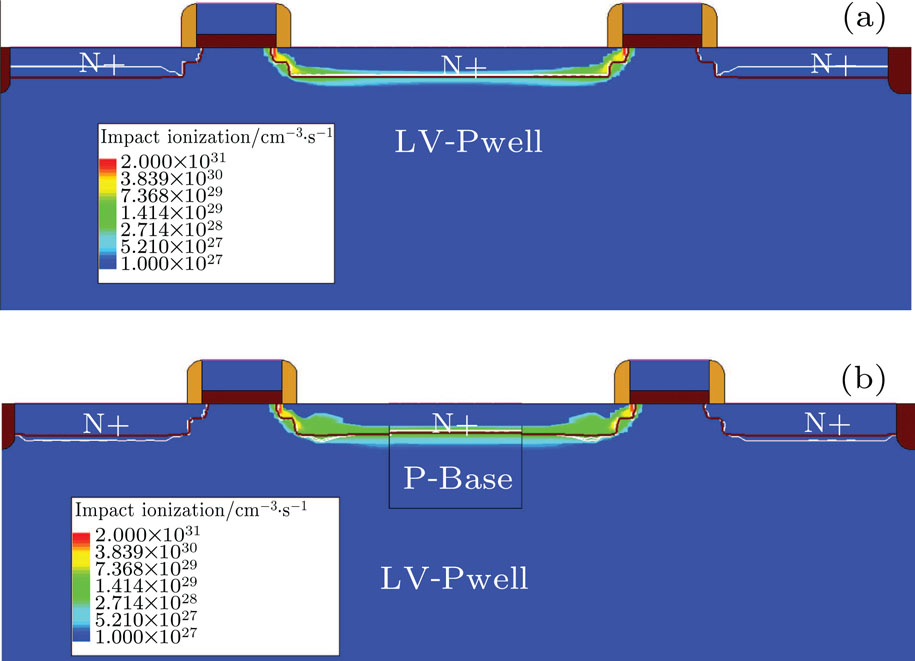
Furthermore, in order to prove the benefits of additional vertical current path in proposed PB-NMOS devices, the impact ionization distributions of conventional GGNMOS and proposed PB-NMOS_type1 are simulated and shown in Figs. 3(a) and 3(b), respectively. Obviously, the impact ionization rate of the reverse biased N+/P-base junction is much higher than that of the N+/LV-Pwell junction, because the N+/P-base junction holds a higher build-up electric field. As a result, a larger proportion of ESD current flows through the vertical NPN path in proposed PB-NMOS_type1, which enhances the robustness of proposed PB-NMOS devices.

Fig. 3. TCAD simulation results of the impact ionization distributions in (a) conventional GGNMOS and (b) proposed PB-NMOS_type1.
3. TLP measurements and discussion

All the conventional GGNMOS and proposed PB-NMOS devices are fabricated in a 0.5- BCD process, with 20 parallel fingers for each device and a device width of 20 for each finger. In addition, all the devices have a fixed drain length of m. Accordingly, all these devices have same layout area. To evaluate the ESD robustness of all these devices, the quasi-static current–voltage (IV) characteristics are measured using the transmission line pulsing (TLP) tester, with a rise time of 10 ns and pulse width of 100 ns. The leakage currents are evaluated at a direct current (DC) voltage of 5 V, which is the operating voltage of protected core circuit.

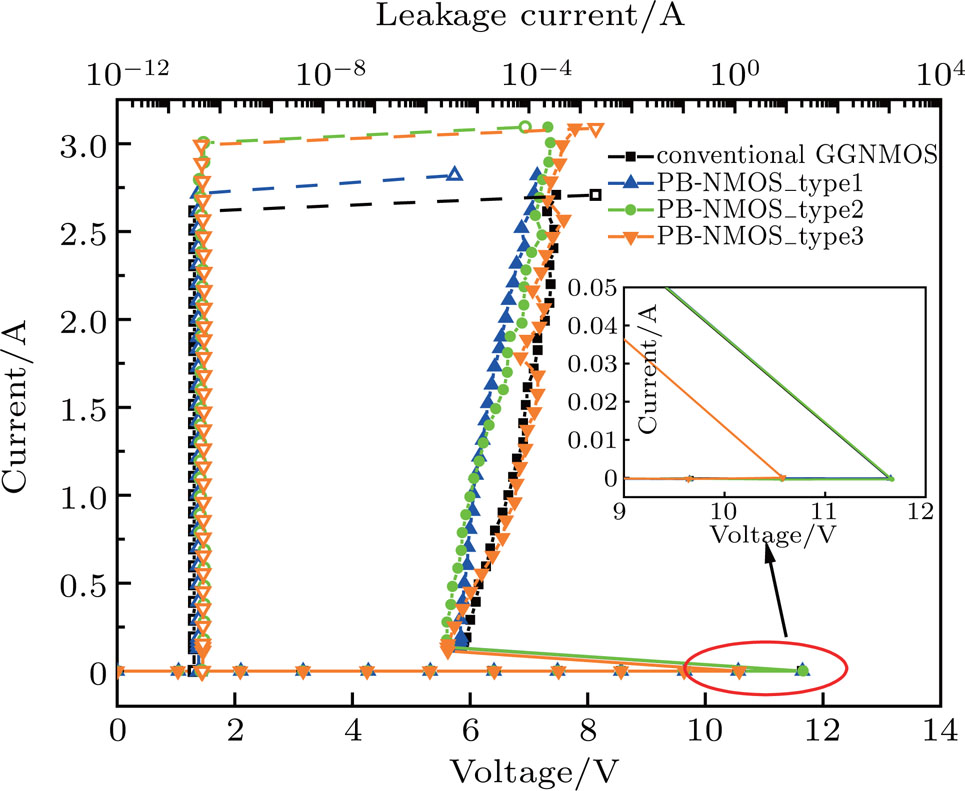
The measured TLP IV curves of the conventional GGNMOS and proposed PB-NMOS devices are illustrated in Fig. 4, and the key ESD parameters are also extracted and listed in Table 1. It can be observed that all the proposed PB-NMOS devices possess higher failure currents (It2) and corresponding enhanced ESD robustness than that of the conventional GGNMOS, thanks to the additional vertical NPN path. In particular, the failure currents of proposed PB-NMOS_type2 and PB-NMOS_type3 can be enhanced by 15.38%, comparing to that of the conventional GGNMOS. It can also be observed that the ESD robustness becomes more prominent as the P-base length increases from PB-NMOS_type1 to PB-NMOS_type2. But the failure current of PB-NMOS_type3 is almost the same as the PB-NMOS_type2, implying that using a larger P-base region beyond the drain region provides no benefit to the ESD robustness.

Fig. 4. TLP IV curves of conventional GGNMOS and proposed three types of PB-NMOS.
Table 1.

Electrical characteristics of the proposed structures and the conventional GGNMOS according to design variable.

.

However, such a surrounding P-base region in PB-NMOS_type3 can reduce the trigger voltage (Vt1) of proposed PB-NMOS_type3, as listed in Table 1. This is attributed to that the P-base layer embedded into the channel region has a heavier doping concentration than that of the LV-Pwell under the gate, which leads to a lower reverse breakdown voltage of N+/P-base junction and a smaller trigger voltage correspondingly. Therefore, the PB-NMOS_type3 is more suitable for ESD protection in 0.5- BCD process, which meets a relatively narrow design window from 5.5 V to about 11 V. It should be noted that the PB-NMOS_type1 and PB-NMOS_type2 have the same trigger voltages as the conventional GGNMOS, which implies that the breakdown voltage of LDD/LV-Pwell junction is smaller than that of the N+/P-base junction.[1]

Leakage current is another critical design metric for the ESD devices. It can be seen that all proposed PB-NMOS devices have approximately the same leakage currents as the conventional GGNMOS, which is an effective improvement of leakage current compared to the GGNMOS with P-ESD implantation.[10] As shown in Fig. 4, all the leakage currents of conventional GGNMOS and proposed PB-NMOS devices are less than 1 nA, which is small enough compared with the operating current of protected core circuit.

From the above discussion, all the proposed PB-NMOS devices are superior to the conventional GGNMOS in ESD robustness. Particularly, PB-NMOS_type3 has the best ESD robustness due to the enhanced ESD characteristics on relatively higher failure current, smaller trigger voltage, and smaller snapback region.

4. Conclusion and perspectives

An enhanced GGNMOS by using the P-base layer called PB-NMOS, has been developed and verified in a 0.5- BCD process in this work. The PB-NMOS is constructed by using the fully process compatible P-base layer to improve the ESD robustness. And it is found that the proposed PB-NMOS devices possess higher ESD robustness than the conventional GGNMOS, without increased layout area, additional process layer, and more cost. In addition, the PB-NMOS device with P-base layer surrounding the entire active area has a reduced trigger voltage, making it more attractive for ESD protection with a smaller design window.

Reference
[1] Wang A 2002 On-Chip ESD Protection For Integrated Circuits Boston Springer pp. 51–59
[2] Leroux C Buj C Chnate J P 1995 Proceedings of the 25th European Solid State Device Research Conference, September 25–27, 1995, Hague, Netherlands p. 321
[3] Song B Han Y Li M Dong S Guo W Huang D Ma F Miao M 2010 Electron. Lett. 46 518 https://doi.org/10.1049/el.2010.0205
[4] Zhou Z Jin X Wang Y 2016 Proceedings of the 13th IEEE International Conference on Solid-state & Integrated Circuit Technology, October 25–28, 2016, Hangzhou, China p. 1
[5] Kim C Park H Kim Y Kang D Lee M Lee S Jeon C Kim H Yoo Y Yoon H 2000 Proceedings of the IEEE Electrical Overstress/Electrostatic Discharge Symposium, September 26–28, 2000, Anaheim, USA p. 26
[6] Li J Alvarez D Chatty K Abou-khalil M J Gauthier R Russ C Seguin C Halbach R 2006 Proceedings of the 13th International Symposium on the Physical and Failure Analysis of Integrated Circuits, July 3–7, 2006, Singapore, Singapore p. 276
[7] Chaing C Chang P Tseng P Lai P Tang T Su K 2016 Proceedings of the IEEE International Reliability Physics Symposium, April 17–21, 2016, Pasadena, USA p. EL.3.1
[8] Chatty K Chatty K Alvarez D Gauthier R Russ C Abou-Khalil M Kwon B J 2007 Proceedings of the 29th Electrical Overstress/Electrostatic Discharge Symposium, September 16–21, 2007, Anaheim, USA p. 7A.2-1
[9] Wang C Chen Y Tang T Su K 2013 Proceedings of the IEEE International Reliability Physics Symposium, April 14–18, 2013, Anaheim, USA p. EL.3.1
[10] Alvarez D Abou-Khalil M J Russ C Chatty K Gauthier R Kontos D Li J Seguin C Halbach R 2006 Microelectron. Rel. 46 1597 https://doi.org/10.1016/j.microrel.2006.07.041
[11] Haken R A Havemann R H Eklund R H Hutter L N 1990 BiCMOS Technology and Applications Boston Springer pp. 63–64