
† Corresponding author. E-mail:
Project supported by the National Key Technology Research and Development Program of China (Grant No. 2018YFA0306101), the National Natural Science Foundation of China (Grant No. 61505196), the Scientific Instrument Developing Project of the Chinese Academy of Sciences (Grant No. YJKYYQ20170032), and the Guangdong Science and Technology Project, China (Grant No. 20180329).
Systematic investigation of InAs quantum dot (QD) growth using molecular beam epitaxy has been carried out, focusing mainly on the InAs growth rate and its effects on the quality of the InAs/GaAs quantum dots. By optimizing the growth rate, high quality InAs/GaAs quantum dots have been achieved. The areal quantum dot density is 5.9 × 1010 cm−2, almost double the conventional density (3.0 × 1010 cm−2). Meanwhile, the linewidth is reduced to 29 meV at room temperature without changing the areal dot density. These improved QDs are of great significance for fabricating high performance quantum dot lasers on various substrates.
In recent years, 1.3-
The growth of InAs on GaAs has a tendency to form islands due to the large lattice mismatch, almost 7.16%, which results in the epitaxial growth transitions from two-dimensional layered growth to three-dimensional island growth. This is the Stranski–Krastanow (S–K) growth mode, which is suitable here for the proposed heterojunction material system with a mismatch in lattice constants but a low interfacial energy.[15] The growth quality of the QDs (dot density and size uniformity) has significant influence on the performance of the final device, as well as affecting the intermediately fabrication processes, thus it is very important to ensure the high quality of QDs in the growth stage.[16,17]
Various investigations of optimizing the parameters have been reported to obtain high quality QDs. Metal–organic chemical vapor deposition (MOCVD) is one of the typical deposition techniques employed.[18,19] However, it is difficult to fabricate arsenic based high performance QD lasers using MOCVD.[20,21] Molecular beam epitaxy (MBE) is a more suitable method, where the interruption growth mode of QDs,[22] growth temperature,[23] and multistacking QD layers[24,25] are methods proposed to enhance the surface dot density. While these do improve the dot density, (4–5) × 1010 cm−2, introduction of singular large QDs is also seen, which then degrades the QD uniformity.[22,23] For further enhancement of the QD quality, this introduction of singular large QDs needs to be suppressed. Various methods such as increasing the surface adatom mobility,[26] introducing a strain reducing layer (SRL),[27] and optimizing the growth rate[14,16,28,29] have been investigated for improving the QD size uniformity. By introducing the strain reducing layer, the linewidth was reduced to 21 meV while the density only achieved 1.0 × 1010 cm−2.[27] A recent study by Liuʼs group systematically improved the dot-height uniformity of QD, obtaining the linewidth of 30 meV with the density of 4.5 × 1010 cm−2 and 42 meV with the density of 5.8 × 10¹⁰ċm−2.[29] Thus far, few comprehensive investigations for improving both dot density and size uniformity have been done. We aim to optimize the growth parameters to obtain high dot density and high size uniformity.
The growth rate of QDs is shown to affect not only the density and uniformity of materials, but also their photoluminescence (PL): if the density of QDs is too high, singular large QDs are formed, resulting in decreased PL intensity and broadened linewidth. In this paper, the influence that the growth rate has on the quality of InAs QDs (on GaAs substrates) via MBE is systematically investigated, with the optimized growth rate determined. Atomic force microscope (AFM) and PL measurements are conducted on the bare QD demonstrating the significant influence that the growth rate has on the QD density, size uniformity, and the optical properties.
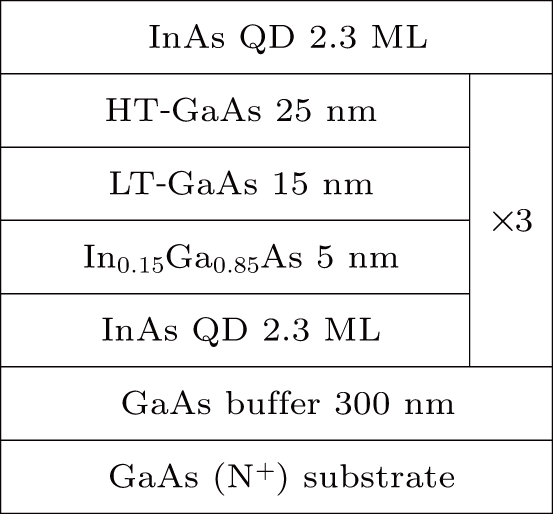
Figure
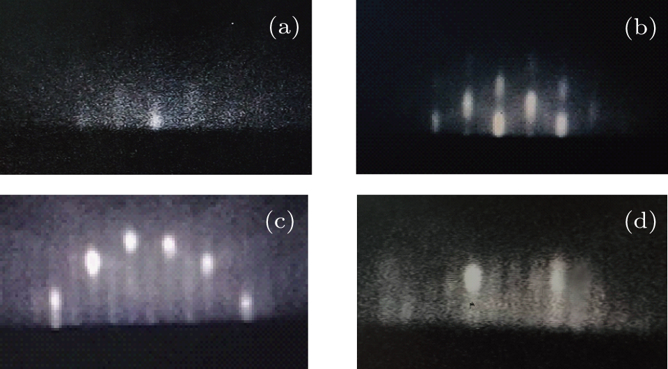
All samples were grown on GaAs (001) n-type substrates using the Gen 930 MBE system from Veeco Instruments equipped with reflective high-energy electron diffractometer (RHEED). The sample was loaded into the MBE chamber with molybdenum adapting plates and in the introduction chamber/buffer chamber, moisture, carbon dioxide, and other impurity on the surface were removed by degassing at a temperature of 200 °C/420 °C. It was then transferred to the growth chamber for oxide desorption at 650 °C under As2-overpressure. Real-time reciprocal space image of the substrate surface was shown through RHEED (Figs.
Finally, other layers of the active region (as shown in Fig.
| Table 1.
The growth parameters of the sample. . |
The AFM images of the uncapped surface QDs in different growth rates are shown in Fig.
| Table 2.
Properties of QDs with different growth rates. . |
The nucleation sites for InAs remain mostly the same regardless of the growth rate. However, under lower growth rates, the relative distance between nucleates is larger (nucleates are smaller), whereas the relative distance between nucleates grown with higher rates is shorter (nucleates are larger). Starting at a low growth rate, the density/uniformity of the QD array is low due to some nucleates growing to islands while others remain very small. As the growth rate increases, the QD array quality increases: each QD is well grown thus the density and uniformity are improved. However, as the growth rate is further increased, the QD array quality decreases again as the islands cluster and fuse to become large QDs. Therefore, there is an optimized growth rate producing high uniformity and dense QD array.
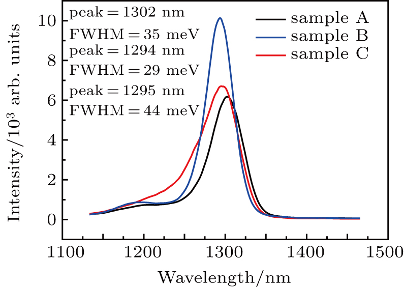
PL measurements under room temperature (RT) were also conducted for the samples, as shown in Fig. 
A series of samples grown at varying InAs QDs growth rates were studied systematically. The growth rate of the QDs significantly influenced the quality of the InAs QDs. The optimized growth rate of 0.06 ML/s produced the best QDs in terms of dot density, size uniformity, and PL spectrum. By optimizing the growth rate, an InAs quantum dot density of 5.9 × 1010 cm−2, almost double the conventional density (3.0 × 1010 cm−2), has been achieved. At the same time, sample B, grown at the rate of 0.06 ML/s, exhibited the strongest PL intensity (1.64 times higher than that of sample A and 1.51 times higher than that of sample C) and narrowest linewidth, 29 meV. This process of optimizing the growth rate for producing high quality InAs QDs (high dot density and size uniformity) will serve as a basis for optimizing the growth of high performance 
The authors appreciate Professor Ying-Qiang Xu for his assistance in MBE maintenance. We also sincerely thank Yi-Feng Song for polishing the manuscript.
| [1] | |
| [2] | |
| [3] | |
| [4] | |
| [5] | |
| [6] | |
| [7] | |
| [8] | |
| [9] | |
| [10] | |
| [11] | |
| [12] | |
| [13] | |
| [14] | |
| [15] | |
| [16] | |
| [17] | |
| [18] | |
| [19] | |
| [20] | |
| [21] | |
| [22] | |
| [23] | |
| [24] | |
| [25] | |
| [26] | |
| [27] | |
| [28] | |
| [29] | |
| [30] | |
| [31] | |
| [32] | |
| [33] | |
| [34] |


