High performance lateral Schottky diodes based on quasi-degenerated Ga2O3
Xu Yang1, Chen Xuanhu1, Cheng Liang1, Ren Fang-Fang1, 2, 3, Zhou Jianjun4, Bai Song4, Lu Hai1, Gu Shulin1, 2, Zhang Rong1, 2, Zheng Youdou1, 2, Ye Jiandong1, 2, 3, †
School of Electronic Science and Engineering, Nanjing University, Nanjing 210093, China
Collaborative Innovation Center of Solid-State Lighting and Energy-Saving Electronics, Nanjing University, Nanjing 210093, China
Research Institute of Shenzhen, Nanjing University, Shenzhen 518057, China
State Key Laboratory of Wide-Bandgap Semiconductor Power Electric Devices, The 55th Research Institute of China Electronics Technology Group Corporation, Nanjing 210016, China


† Corresponding author. E-mail: yejd@nju.edu.cn

Project supported by the National Key R&D Program of China (Grant No. 2017YFB0403003), the National Natural Science Foundation of China (Grant Nos. 61774081, 61322403, and 91850112), the State Key R&D Project of Jiangsu, China (Grant No. BE2018115), Shenzhen Fundamental Research Project, China (Grant Nos. 201773239 and 201888588), State Key Laboratory ofWide-Bandgap Semiconductor Power Electric Devices, China (Grant No. 2017KF001), and the Fundamental Research Funds for the Central Universities, China (Grant Nos. 021014380093 and 021014380085).

Abstract

Ni/β-Ga2O3 lateral Schottky barrier diodes (SBDs) were fabricated on a Sn-doped quasi-degenerate n+-Ga2O3 bulk substrate. The resultant diodes with an area of 7.85×10⁻⁵ cm2 exhibited excellent rectifying characteristics with an ideality factor of 1.21, a forward current density (J) of 127.4 A/cm2 at 1.4 V, a specific on-state resistance (Ron,sp) of 1.54 mΩ.cm2, and an ultra-high on/off ratio of 2.1×10¹¹ at ±1 V. Due to a small depletion region in the highly-doped substrate, a breakdown feature was observed at −23 V, which corresponded to a breakdown field of 2.1 MV/cm and a power figure-of-merit of 3.4×10⁵ W/cm2. Forward current–voltage characteristics were described well by the thermionic emission theory while thermionic field emission and trap-assisted tunneling were the dominant transport mechanisms at low and high reverse biases, respectively, which was a result of the contribution of deep–level traps at the metal–semiconductor interface. The presence of interfacial traps also caused the difference in Schottky barrier heights of 1.31 eV and 1.64 eV respectively determined by current–voltage and capacitance–voltage characteristics. With reduced trapping effect and incorporation of drift layers, the β-Ga2O3 SBDs could further provide promising materials for delivering both high current output and high breakdown voltage.

1. Introduction

Ultra-wide bandgap (UWBG) semiconductors are promising for the delivery of power electronic devices and deep-ultraviolet solar-blind photodetectors with high energy conversion efficiency which have versatile applications in electric power, industrial control, consumer electronics, automotive electronics industries, flame detection, missile guidance, biochemical detection, and space communication.[17] Among these UWBG materials, β-Ga2O3 is attracting significant interest owing to its highly projected Baliga’s figure-of-merit (FOM) as a result of its wide-bandgap of 4.9 eV and large theoretical breakdown field of 8 MV/cm.[811] This is well in excess of the values of SiC and GaN, both of which are now established with commercial availability for high power devices. As β-Ga2O3 is one of the intrinsic solar-blind materials, state-of-the-art solar-blind photodetectors based on β-Ga2O3 Schottky diodes have been reported.[1214] Compared to other UWBG materials including diamond and AlN, the availability of melt-growth methods to mass-produce single crystal β-Ga2O3 bulk substrates and the easy control of n-type doping provide important benefits towards low cost as well as the rapid development of epitaxial growth and device technologies. In recent years, rapid progress on the performance of field-effect transistors (FETs) and Schottky barrier diodes (SBDs) has been made.[1522] With a low-doped drift layer grown by hydride vapor phase epitaxy (HVPE) and the integration of the field plates, vertical Schottky rectifiers with a breakdown voltage (VB) of over 1 kV have been demonstrated.[15] Very recently, with the employment of a trench structure, SBDs without optimized field management techniques showed a 1230 V breakdown voltage and a decent on-resistance (Ron,sp = 15 mΩ·cm2).[16] There are also recent advances in the edge termination method that suppress the electric field and enhance the reverse breakdown voltages.[1722]

One of the merits of UWBG semiconductor-based SBDs is the improvement of their efficiency for applications in invertor circuits which need high current output. To date, most of the reported β-Ga2O3 SBDs are based on an unintentionally doped single crystal or thick epitaxial drift layer with a low carrier concentration. As a result, while the diode sustains extremely high critical electric fields, leading to large blocking voltages, high current output is limited. A trade-off between high breakdown voltage and high forward current output remains an unsolved issue. Further improvement in the efficiency and functionality of invertors relies on high current output and speed, which can be realized by low on-state resistances using highly-doped wide-bandgap semiconductors. However, SBDs directly fabricated on highly-doped quasi-degenerated Ga2O3 materials are still challenging. Recently, only Oishi et al. reported on the fabrication of vertical SBDs directly on β-Ga2O3 single crystals with a high electron concentration of 3.9×1018 cm−3.[23] Despite the fact that the diodes exhibit clear rectification characteristics with a current density of 96.8 A/cm2 at the forward voltage of 1.6 V, there is still much room for improvement in the device performance, and also the conduction mechanism of devices on quasi-degenerated β-Ga2O3 is not fully understood. In this work, we demonstrated improved performance of SBDs in lateral configurations on a weakly-degenerated β-Ga2O3 ( ) single crystal substrate with a high carrier concentration of 2×1018 cm−3. The resultant lateral diodes showed excellent rectifying characteristics with an ultra-high rectification ratio of 2.1×10¹¹ at ±1 V, an ideality factor of 1.21, a forward current density of 127.4 A/cm2 at 1.4 V, and a specific on-state resistance Ron,sp of 1.54 mΩ·cm2. Furthermore, the associated transport mechanisms have been investigated in detail by means of current–voltage and capacitance–voltage characterizations.

2. Experimental details

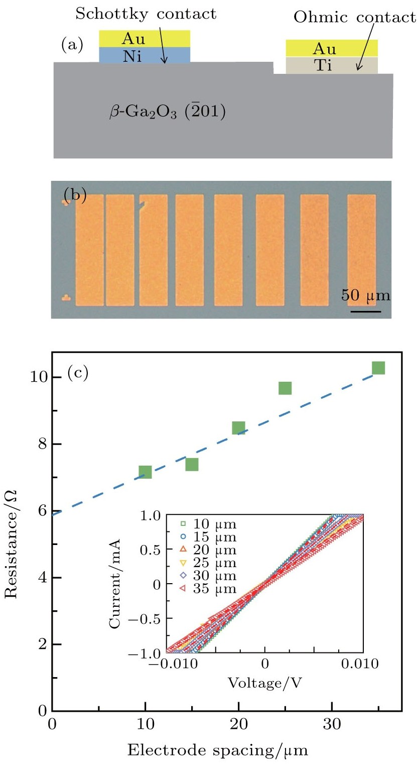
All bulk substrates used in this work were square-shaped pieces cut from commercial 2-inch diameter, 500 μm-thick Sn-doped n-type 9 β-Ga2O3 wafers with a carrier concentration of 2 × 1018 cm−3 grown by the edge-defined film-fed growth (EFG) method. After chemically cleaning the β-Ga2O3 substrates with acetone, ethanol, and deionized water and subsequent lithography processing, the surface was selectively etched by an inductively coupled plasma (ICP) technique using a BCl3 gas with a flow of 20 sccm for 80 s under a plasma/bias power of 400 W/30 W. The etch rate was measured at 15 nm/min using a profilometer. Then, Ti/Au metal stacks (100 nm/100 nm) were deposited by electron beam evaporation and annealed in nitrogen ambient at 650 °C for 60 s to ensure good Ohmic contacts. Subsequently, Ni/Au metal stacks (100 nm/100 nm) were selectively deposited as Schottky electrodes using an e-beam evaporator on the same side of the substrate by following a standard lithography procedure. Finally, through liftoff processes, circular Schottky contacts with diameters of 100 μm were formed. Figure 1(a) is a schematic of the planar β-Ga2O3 SBDs. The current–voltage (IV) characteristics were measured using a Keithley source meter (model 2636A) and the capacitance–voltage (CV) measurements were performed using a Keithley source meter model 4980A at the high frequency of 100 kHz. All measurements were performed at room temperature.

Fig. 1. (a)The geometry of the fabricated Schottky diodes. (b) Optical microscopy image of the TLM structures. (c) Total resistance between Ti/Au electrode spacing for ND=2×1018 cm−3. The inset shows the IV characteristics with different electrode spacings.
3. Results and discussion

Transmission line measurement (TLM) methods were employed to characterize the specific contact resistivity of the Ohmic electrodes. The electrodes for TLM tests are Ti/Au metal stacks (100 nm/100 nm) which were fabricated and annealed under the same conditions as the Ohmic contacts described above. The rapid thermal annealing process has been optimized with the condition of 650 °C for 60 s to reduce the contact resistance. It was found that surface pre-treatment by ICP processing increased the surface roughness and generated large-density donor-like surface defects, which is helpful for enhancing the Ohmic features and decreasing the contact resistance.[24] After ICP treatment, TLM structures with channel lengths varying from 10 μm to 35 μm were fabricated, as shown in Fig. 1(b). Figure 1(c) and its inset show the total resistance as a function of the channel length and the current–voltage behavior of the Ti/Au contacts with different channel lengths, respectively. Linear IV features with different channel lengths are observed, indicating the nature of Ohmic contact to β-Ga2O3 by Ti/Au metal stacks. The total resistance between the electrodes is almost a linear function of the channel spacing. From Fig. 1(c), the sheet resistance (Rs) and specific contact resistance (Rc) were extracted to be 24.3 Ω/▭ and 1.42 ×10⁻⁴ Ω·cm2, respectively.

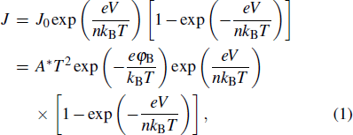
Figure 2 and its inset show the linear plot and semi-logarithmic plot of the JV characteristics of the β-Ga2O3-based planar Schottky diodes with a diameter of 100 μm measured at room temperature (RT). In this work, the clamp current, which was set at 10 mA, was achieved at 1.4 V. Given the density of states (DOS) of the conduction band minimum (CBM) (NC=3.8×1018 cm−3) for the β-Ga2O3 and a carrier concentration of 2×1018 cm−3, the energy difference between the CBM and the Fermi level is about 23.7 meV, which is less than kBT and indicative of weak degeneration of the β-Ga2O3 substrate. As a result, the large forward current density of 127.4 A/cm2 was achieved at a rather small applied voltage of 1.4 V, which is much higher than other reported current densities. In particular, the main challenge of Schottky contact to a weak degenerated substrate is to maintain excellent rectifying features with low leakage currents due to a small depletion region and a high possibility of quantum tunneling transport across the barrier. A low leakage current density of 6×10⁻¹⁰ A/cm2 at −1 V, reaching the measurement limitation of the source meter, was measured. It resulted in a high on/off current ratio up to 2.1×10¹¹, which is, to the best of our knowledge, one of the highest reported rectification ratios in β-Ga2O3-based Schottky devices. As shown in the inset of Fig. 2, the ideal thermionic emission (TE) theory could be used to fit well the relationship between the forward current density and voltage[23]

where e, n, kB, h, T, J0, A∗, m, and φB are the elementary charge, the ideality factor, the Boltzmann constant, the Plank constant, the temperature, the saturation current density, the effective Richardson constant, the electron effective mass, and the Schottky barrier height at equilibrium, respectively. The electron effective mass used of β-Ga2O3 is m = 0.34 m0, with m0 being the free electron mass, and the value of A is 40.8 A/cm2·K2.[23] When V >3kBT/e (∼ 0.078 V at room temperature), equation (1) can be simplified as
Determined from Eq. (3), the ideality factor n is inversely proportional to the slope of the ln(J)–V curve and fitting to the linear zone in the inset of Fig. 2 gives rise to the ideality factor n = 1.21. The causes of the n value being larger than 1 (unity) could be thermionic field emission tunneling, edge leakage, trap-assisted tunneling, and so forth, which tend to degrade the electron device performance characteristics. The saturation current density of 4.04 ×10⁻¹⁶ A/cm2 and a Schottky barrier height of 1.31 eV can also be calculated, consistent with other reported values. Extracted by extrapolation from the linear zone in Fig. 2, the values of threshold voltage and on-resistance were obtained as 1.22 V and 1.54 mΩ·cm2, respectively. Therefore, a low on-resistance and a small ideality factor prove the high conduction performance of the Schottky barrier diodes with Ni contacts upon forward bias. Reverse JV characteristics of the Schottky barrier diode are shown in Fig. 3(a). The leakage current began to increase rapidly at −11 V and the results are repeatable. In the linear plot shown in Fig. 2, the current density increases sharply at −23 V with a length of depletion layer of 116 nm, a corresponding electric field of 2.10 MV/cm and a power figure-of-merit ( ) of 3.4×10⁵ W/cm2.

Linear plot of JV characteristics of the β-Ga2O3-based Schottky diodes with a diameter of 100 μm measured at room temperature. The inset is the semi-logarithmic plot of forward JV.

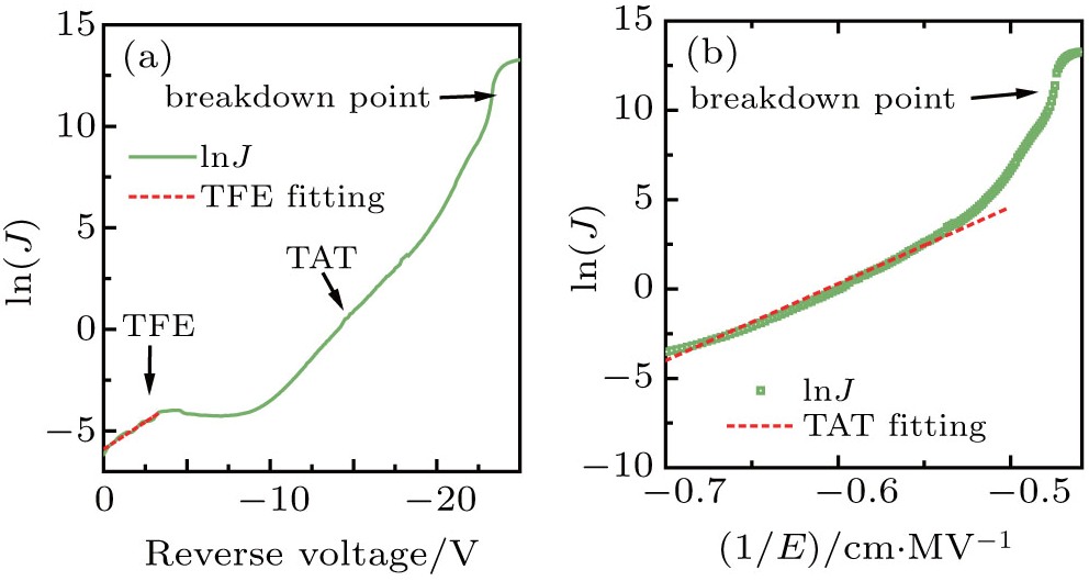
To evaluate the plausibility of various conduction mechanisms responsible for the observed leakage current, analytical modeling of electrical transport properties in reverse bias is necessary. For highly-doped weak-degenerated β-Ga2O3, the tunneling probability increases as electrons see a thinner barrier. It has been widely reported that the tunneling through thermionic field emission (TFE) becomes the favored transport phenomenon at reverse biases especially for high doping and intermediate temperatures.[25] Thermionic field emission takes place between field emission and thermionic emission.[25] When kBTE00, the tunneling electrons have energy between the Fermi level of the metal and the conduction band edge of the dielectric. In this work, the current density at reverse bias below −4 V could be fitted well by the TFE model, which is given by[26]

where J00, V, ε, E00, , ND, m, and εs ε0 are the saturation current density, the applied reverse bias, a temperature-dependent energy parameter that depends on the semiconductor doping, the Planck constant, the donor density, the electron effective mass, and the dielectric constant of the semiconductor, respectively. As shown in Fig. 3(a), the ln(J)–V plot can be fitted well by the TFE model at biases lower than 4 V and the slope of the linear variation of ln(J)–V allows the determination of the E00 parameters. The evaluated E00 value is 5.4 meV at room temperature, which is comparable to the thermal energy of kBT = 26 meV at RT. Therefore, the observed exponential increase of the reverse leakage currents in the low reverse bias regime is governed by the tunneling transport mechanism through the TFE process as would be expected in most wide bandgap semiconductor-based Schottky diodes.

Furthermore, the evolution of reverse current at the high bias exhibits rather weak dependence on the applied voltages, which has also been observed in AlGaN-based Schottky diodes and is possibly contributed to by various field-enhanced tunneling mechanisms, such as the Pool–Frenkel (PF) emission, Fowler–Nordheim (FN) tunneling, or trap assisted tunneling (TAT) mechanisms.[25] When the reverse voltage is higher than −11 V, the length of the depletion layer is calculated to be larger than 80 nm and increases with the elevated bias. It was reported that the FN tunneling model becomes the dominant transport mechanism when the barrier is thin enough (< 100 Å).[27] Thus, the FN mechanism can be excluded and the PF emission model was also found to fail to describe the leakage current at high reverse bias.[2830] As a matter of fact, the current transport can be understood well by the TAT mechanism as expressed by[3132]

where ATATmE, and φr are a constant, the electron effective mass, the electric field, and the energy of the electron traps with respect to the conduction band edge of the dielectric, respectively. It indicates that ln J varies linearly with φr3/2, which can be observed in the JV characteristics of the device as shown in Fig. 3(b). The plot of ln J versus 1/E shows a good linear feature, and thus φr is extracted to be 1.05 V at high field values. The above analysis suggests that the interface traps are present at the metal–semiconductor interface, which reduce the Schottky barrier height or narrow the depletion region, leading to the carrier tunneling and large leakages. When the electric field approaches the breakdown point, the tunneling breakdown would possibly occur, leading to the remarkable increase in reverse leakage current, as shown in the part that does not follow the TAT model in Fig. 3(b).

Fig. 3. (a) Linear fitting of ln(J)–V at low field by TFE and (b) linear fitting of ln(J)–1/E at relatively high field by TAT.

Figure 4(a) shows the CV and 1/C2V plots of the Schottky barrier diodes measured at room temperature with 100 kHz sampling frequency. The capacitance decreases from 2.9 ×10⁻⁷ F/cm2 to 1.44 ×10⁻⁷ F/cm2 when the reverse bias is changed from 0 to −5 V due to the expanded depletion layer. The relationship between 1/C2 and the applied voltage can be expressed as[24]

where ѱbi, qA, and ND are the built-in voltage of the diode, the elementary charge, the contact area, and the electron concentration, respectively. Therefore, ѱbiND can be calculated from the intercept and the slope of a plot of 1/C2V, respectively. The value of ND extracted from the slope is about 1.96×1018 cm−3, which is consistent with the Hall measurement results of the substrate given by Tamura Corporation, Japan. The Schottky barrier height is related to the built-in voltage and carrier concentration as given by[24]
where ECEF, and NC are the conduction band minimum, the Fermi level, and the effective density of the states in the conduction band, respectively. The Schottky barrier height calculated from the CV curve is 1.64 eV, which is higher than the one obtained from the forward JV characteristics. The schematic energy band diagram of the Schottky contact between Ni and β-Ga2O3 is shown in Fig. 4(b). One cause of the difference in the barrier heights obtained from the IVCV curves is the image force lowering effect, which normally affects the JV characteristics with a negative effect on the barrier height while the CV measurement at high frequency remains unaffected. However, the reduction in barrier height due to the image force lowering effect in this work is calculated to be only 0.125 eV, much smaller than the barrier difference of about 0.33 eV. Thus, image force lowering is not the main cause. It has been reported that the existence of interface traps could be the dominant cause of the difference.[3334] As a result, the corresponding breakdown field is still lower than the expected theoretical value of 8 MV/cm. It is thus necessary to

(a) The CV characteristics and 1/C2V plots of the Schottky barrier diodes at room temperature with 100 kHz sampling frequency. (b) Schematic energy band diagrams of the Schottky contact between Ni and β-Ga2O3.

improve the interface quality of the metal–semiconductor contact to decrease the interface traps.

4. Conclusions

Planar geometry Schottky diodes were fabricated based on highly-doped β-Ga2O3 ( ) substrates with an ultra-high rectification ratio of 2.1 × 10¹¹, a high current density of 127.4 A/cm2 at 1.4 V, a low leakage of 6 × 10⁻¹⁰ A/cm2, an ideality factor of 1.21, a low specific on-resistance of 1.54 mΩ·cm2, and a power figure-of-meri( ) of 3.4×10⁵ W/cm2. The Schottky barrier height was calculated to be 1.31 eV and 1.64 eV from the IV and CV curves, respectively, and the difference mainly resulted from the existence of interface traps. Forward IV characteristics were described well by the thermionic emission theory while thermionic field emission and trap-assisted tunneling are the dominant transport mechanisms at low and high reverse biases, respectively, which is a result of the contribution of deep-level traps at the metal–semiconductor interface. With reduced trapping effect, the performance of β-Ga2O3 SBDs could be further improved to deliver both high current output and high breakdown voltage.

Reference
[1] Yang C Liang H Zhang Z Xia X Tao P Chen Y Zhang H Shen R Luo Y Du G 2018 RSC Adv. 8 6341
[2] Jang S Jung S Kim J Ren F Pearton S J Baik K H 2018 ECS J. Solid State Sc 7 Q3180
[3] Oshima T Hashiguchi A Moribayashi T Koshi K Sasaki K Kuramata A Ueda O Oishi T Kasu M 2017 Jpn. J. Appl. Phys. 56 086501
[4] Oh S Yang G Kim J 2017 ECS J. Solid State Sc 6 Q3022
[5] Oishi T Koga Y Harada K Kasu M 2015 Appl. Phys. Express 8 031101
[6] Higashiwaki M Konishi K Sasaki K Goto K Nomura K Thieu Q T Togashi R Murakami H Kumagai Y Monemar B 2016 Appl. Phys. Lett. 108 133503
[7] Liu Z Li P G Zhi Y S Wang X L Chu X L Tang W H 2019 Chin. Phys. 28 017105
[8] Hu Z Zhou H Feng Q Zhang J Zhang C Dang K Cai Y Feng Z Gao Y Kang X 2018 IEEE Electron Device Lett. 39 1564
[9] Yang J C Ahn S Ren F Pearton S J Jang S Kim J Kuramata A 2017 Appl. Phys. Lett. 110 192101
[10] Farzana E Zhang Z Paul P K Arehart A R Ringel S A 2017 Appl. Phys. Lett. 110 202102
[11] Ahn S Ren F Yuan L Pearton S Kuramata A 2017 ECS J. Solid State Sc 6 P68
[12] Oshima T Okuno T Arai N Suzuki N Hino H Fujita S 2009 Jpn. J. Appl. Phys. 48 011605
[13] Suzuki R Nakagomi S Kokubun Y Arai N Ohira S 2009 Appl. Phys. Lett. 94 222102
[14] Pratiyush A S Xia Z Kumar S Zhang Y Joishi C Muralidharan R Rajan S Nath D N 2018 IEEE Photon. Technol. Lett. 30 2025
[15] Konishi K Goto K Murakami H Kumagai Y Kuramata A Yamakoshi S Higashiwaki M 2017 Appl. Phys. Lett. 110 103506
[16] Li W Hu Z Nomoto K Zhang Z Hsu J Y Thieu Q T Sasaki K Kuramata A Jena D Xing H G 2018 Appl. Phys. Lett. 113 202101
[17] Yang J Ahn S Ren F Pearton S Jang S Kuramata A 2017 IEEE Electron Device Lett. 38 906
[18] Yang J C Ren F Tadjer M Pearton S J Kuramata A 2018 AIP Adv. 8 055026
[19] Joishi C Rafique S Xia Z Han L Krishnamoorthy S Zhang Y Lodha S Zhao H Rajan S 2018 Appl. Phys. Express 11 031101
[20] Sasaki K Wakimoto D Thieu Q T Koishikawa Y Kuramata A Higashiwaki M Yamakoshi S 2017 IEEE Electron Device Lett. 38 783
[21] Kasu M Oshima T Hanada K Moribayashi T Hashiguchi A Oishi T Koshi K Sasaki K Kuramata A Ueda O 2017 Jpn. J. Appl. Phys. 56 091101
[22] Kasu M Hanada K Moribayashi T Hashiguchi A Oshima T Oishi T Koshi K Sasaki K Kuramata A Ueda O 2016 Jpn. J. Appl. Phys. 55 1202BB
[23] Oishi T Harada K Koga Y Kasu M 2016 Jpn. J. Appl. Phys. 55 030305
[24] He Q Mu W Dong H Long S Jia Z Lv H Liu Q Tang M Tao X Liu M 2017 Appl. Phys. Lett. 110 093503
[25] Rathkanthiwar S Kalra A Solanke S V Mohta N Muralidharan R Raghavan S Nath D N 2017 J. Appl. Phys. 121 164502
[26] Hudait M Krupanidhi S 2001 Phys. B: Condens. Matter 307 125
[27] Chiu F C 2014 Adv. Mater. Sci. Eng. 7 1
[28] Arslan E Bütün S Ozbay E 2009 Appl. Phys. Lett. 94 142106
[29] Zhang H Miller E J Yu E T 2006 J. Appl. Phys. 99 023703
[30] Sun X Li D Jiang H Li Z Song H Chen Y Miao G 2011 Appl. Phys. Lett. 98 121117
[31] Sang L W Ren B Sumiya M Liao M Y Koide Y Tanaka A Cho Y J Harada Y Nabatame T Sekiguchi T Usami S Honda Y Amano H 2017 Appl. Phys. Lett. 111 122102
[32] Sang L Liao M Koide Y Sumiya M 2011 Appl. Phys. Lett. 98 103502
[33] Freeouf J L Jackson T N Laux S E Woodall J M 1982 J. Vac. Sci. Technol. 21 570
[34] Ohdomari I Tu K N 1980 J. Appl. Phys. 51 3735