Negative differential resistance and quantum oscillations in FeSb2 with embedded antimony
Tang Fangdong1, 2, Du Qianheng3, 4, Petrovic Cedomir3, 4, Zhang Wei1, He Mingquan5, Zhang Liyuan2, †
Department of Physics and Beijing Key Laboratory of Optoelectronic Functional Materials & Micro-nano Devices, Renmin University of China, Beijing 100872, China
Department of Physics, Southern University of Science and Technology, and Shenzhen Institute for Quantum Science and Engineering, Shenzhen 518055, China
Condensed Matter Physics and Materials Science Department, Brookhaven National Laboratory, Upton, New York 11973, USA
Department of Materials Science and Chemical Engineering, Stony Brook University, Stony Brook, New York 11790, USA
Chongqing Key Laboratory of Soft Condensed Matter Physics and Smart Materials, College of Physics, Chongqing University, Chongqing 401331, China


† Corresponding author. E-mail: zhangly@sustc.edu.cn

Project supported by Guangdong Innovative and Entrepreneurial Research Team Program, China (Grant No. 2016ZT06D348), the National Natural Science Foundation of China (Grant No. 11874193), and the Shenzhen Fundamental Subject Research Program, China (Grant Nos. JCYJ20170817110751776 and JCYJ20170307105434022). The work at Brookhaven is supported by the US Department of Energy, Office of Basic Energy Sciences as part of the Computational Material Science Program (material synthesis).

Abstract

We present a systematical study on single crystalline FeSb2 using electrical transport and magnetic torque measurements at low temperatures. Nonlinear magnetic field dependence of Hall resistivity demonstrates a multi-carrier transport instinct of the electronic transport. Current-controlled negative differential resistance (CC-NDR) observed in current–voltage characteristics below ∼ 7 K is closely associated with the intrinsic transition ∼ 5 K of FeSb2, which is, however, mediated by extrinsic current-induced Joule heating effect. The antimony crystallized in a preferred orientation within the FeSb2 lattice in the high-temperature synthesis process leaves its fingerprint in the de Haas-Van Alphen (dHvA) oscillations, and results in the regular angular dependence of the oscillating frequencies. Nevertheless, possible existence of intrinsic non-trivial states cannot be completely ruled out. Our findings call for further theoretical and experimental studies to explore novel physics on flux-free grown FeSb2 crystals.

1. Introduction

FeSb2 exhibits a colossal Seebeck coefficient at low temperatures.[1,2] Electronic transport and magnetic measurements closely resemble rare-earth Kondo insulator, such as SmB6, YbB12, Ce3Bi4Pt3, and so on.[36] In a Kondo insulator, the hybridization of localized 4f states and d conduction bands drives the formation of a small insulating gap causing a metal-to-insulator transition (MIT) at low temperature, as in SmB6.[7] Besides the 4f electron system, iron-based Kondo insulator description is proposed for materials with localized 3d electron and noncubic lattice structure, such as FeSi and Fe2VAl.[810] FeSb2 features similar structure and physical properties with FeSi, and thus attracts considerable attention.[1114]

Electrical transport measurements performed by several groups show a multi-carrier nature in FeSb2, accompanied by at least two main energy gaps of ∼ 30 meV and ∼ 5 meV.[1517] From magnetic measurement, the thermally induced paramagnetic moment has been observed, as expected in Kondo insulator.[11,12] The colossal Seebeck coefficient of ∼ −45 mV/K near 10 K and high thermoelectric power factor (TPF) of ∼ 2300 μW/(K2 · cm), are the highest recorded in any material.[1,2] Nonetheless, these properties are highly sample- and impurity-dependent.[18,19] To date, the physical mechanism causing such high value of S is unresolved and could include electronic diffusion with strong correlations,[1,19,20] or phonon-drag effect.[2,21]

In this paper, we have investigated the electrical transport and magnetization properties on FeSb2 single crystals. Arrhenius plot and two-carrier model analyses are performed to obtain the band gaps and carrier information. Observation of current-controlled negative differential resistance (CC-NDR) may suggest some nonlinear dynamic characteristic at first glance. However, by careful experiments, an origin of thermal heating effect is identified. The de Haas-Van Alphen (dHvA) oscillations are observed in the magnetic torque measurements, which correspond to antimony crystallized in preferred orientation within the FeSb2 crystal during the crystal growth process.

2. Experimental methods

FeSb2 single crystals were prepared by the method described in Refs. [11] and [12], then the as-grown crystals were oriented using a Laue camera and cut into small pieces with typical size of 0.8 mm × 0.4 mm × 0.1 mm. Electrical transport measurements were performed using standard four-probe method in an Oxford TeslatronPT cryostat with variable temperatures from 1.5 K to 300 K and a magnetic field up to 14 T. The current–voltage (IV) characteristics were performed using the combination of Keithley 6221 current source and 2182A nanovoltmeter. The commercial Cernox thermometers were used to measure the temperature of the sample during the current–voltage measurements. Magnetic torque measurement was carried out using a homemade capacitance torque magnetometer similar as Ref. [35] [see Figs. 4(a) and 4(b)]. The sample was glued onto the tip of a thin brass cantilever, and by tracking the capacitance between the cantilever and a gold film underneath, the magnetic torque can be measured in high accuracy. Choosing proper thickness and length of the thin brass can optimize the sensitivity of the torque magnetometer. The capacitance was measured using an AH 2700A ultra-precision 50 Hz–20 kHz capacitance bridge at a frequency from 1 kHz to 5 kHz. Finally, the sample components were checked using energy dispersive x-ray spectroscopy (EDS) measurement in an FEI nova nanoSEM 450.

3. Results and discussion
3.1. Magnetotransport properties

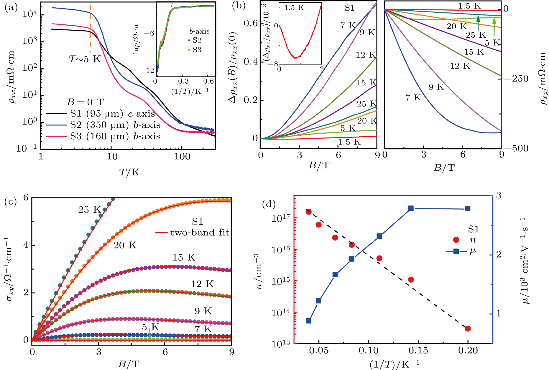
Figure 1(a) displays the temperature dependence of the resistivity of three typical samples. The resistivity of sample 1 (S1) was measured along c axis whereas for sample 2 (S2) and sample 3 (S3), the b axis resistivity is presented. Similar trend is seen, i.e., the resistivity shows semiconducting behavior in the whole temperature range, although anisotropies exist between different samples and different crystal axes. The resistivity saturates below 5 K, indicating the existence of a conductive state, which may be induced by impurity states located in band gap.[15,17] By applying the Arrhenius plot of the temperature-dependent resistivity (lnρ(T) ∝ (Δ/2kB)T−1),[15,17] the thermal activation energy gap can be determined. As shown in the inset of Fig. 1(a), two gaps show up by applying the scaling within two different temperature intervals. The gap around ∼ 28 meV fitted in the range of 40 K ∼ 100 K is the intrinsic energy gap between the valence and conduction band. The gap of ∼ 6 meV for 5 K ∼ 12 K corresponds to the gap between the extinct impurity level and the conduction band.[15,17,21]

Fig. 1. Magnetotransport properties of FeSb2 single crystals. (a) The temperature dependence of the resistivity of three FeSb2 samples (S1, S2, and S3). Inset: Arrhenius plot lnρ(T)∝ T−1 of the temperature regimes where ρ(T) is dominated by thermally activated transport, yields gap one ∼ 28 meV for 40 K–100 K and gap two ∼ 6 meV for 5 K–12 K regime. (b) The magnetoresistivity Δρ/ρ and Hall resistivity as a function of magnetic field at various temperatures. Left inset: zoom in of the 1.5 K curve shows weak localization effect. (c) Two-carrier model analysis of the magnetic field dependence of the conductivity tensor σxy from 5 K to 25 K for S1. (d) 1/T dependence of the carrier density and mobility for the dominating band 1 with higher mobility evaluated from panel (c). The dashed black line describes a thermal activation formulation n ∝ exp(−Δ/2kBT), with Δ ∼ 8.6 meV.

Magnetoresistivity (MR) ρxx and Hall resistivity ρxy measured at low temperatures for S1 are illustrated in Fig. 1(b), from which the basic carrier information of our crystals can be extracted. Multi-carrier transport behavior at temperature higher than 5 K is clearly demonstrated by the nonlinear Hall resistivity and quasi B2 law of MR. In order to track the carrier information of the two energy bands, we employ the standard two-carrier model as[22,23]

Each band has two parameters, resistivity ρi = 1/niqiμi and Hall coefficient Ri = 1/niqi, where qi = ±e(i = 1, 2) is the charge of the carrier, ni is the carrier density and μi is the mobility. This model describes both λxx and λxy very well within a wide temperature range, and in Fig. 1(c) we plot the fitting results of λxy. Both bands are electron type in which band 1 has higher mobility μ1 ∼ 103 cm2 · V−1 · s−1 while lower mobility μ2 ∼10 cm2·V−1·s−1 is found for band 2 around 5 K. Large uncertainties appear for band 2 below 9 K due to the increasingly large mobility difference between the two bands. Band 1 becomes dominant at sufficiently low temperature. Herein we only focus on the high-mobility band 1, and the obtained carrier density and mobility are summarized in Fig. 1(d) as a function of inverse temperature. These results agree well with earlier reports.[15,17] We note that the carrier density and mobility are rather sample-dependent caused by the various impurity concentrations. The carrier density falls onto a single line [dashed line in Fig. 1(d)] when plotted as log(n) versus T−1, from which one can evaluate the thermal activation energy according to n ∝ exp(−Δ / 2kBT), yielding a gap value of ∼ 8.6 meV. This is in well consistent with previous ρ(T) analysis at low temperatures (5 K∼ 12 K).[15,17]

However, below 5 K, the two-carrier model is not applicable since the quantum coherence effect dominates the transport. Low-field negative MR appears in this temperature regime [see the inset of Fig. 1(b)], which is probably caused by weak localization effect of phase-coherence transport of the remaining electrons.[15,17,24] However, the origin of the remaining conducting carriers is still unknown, they may come from the impurity level,[15] or potential topological surface states.[3] Weak localization effect happens when the carriers are weakly localized by random potential, which also exists in three-dimensional systems, such as doped semiconductors.[25,26] Further detailed experimental and theoretical studies are desired to clarify the underlying mechanism of weak localization effect as well as the origin of the remaining carriers in FeSb2 system.

3.2. Negative differential resistance

After obtaining the basic carrier information of the energy bands, we perform further current–voltage measurements to study the nonlinear characteristic of this material. Current-controlled negative differential resistance (CC-NDR) is clearly observed in our measurements. This exotic phenomenon has been reported experimentally in multiple material systems since the early 1960s, such as the oxides of V, Ti, Fe, and many other transition metals.[2730] And theoretically, various mechanisms have also been proposed.[2730] Most of these materials undergo a sharp metal-to-insulator transition (MIT) upon cooling and the observed CC-NDR in these systems naturally suggests the current-induced self-heating effect.[28,30,31] When a large current is applied, the sample is locally warmed up until the critical MIT temperature, above which the resistivity drops abruptly. This has an unstable positive feedback effect on the current and results in the formation of new conductive channels in bulk material.

Figure 2(a) displays the current–voltage (IV) curves recorded at various temperatures from 3.5 K to 15 K of sample 4 using four-terminal geometry. By sweeping up the bias current, the voltage climbs up rapidly in ohmic regime until a critical maximum is reached. It then drops gradually and enters a negative differential resistance regime (NDR). The voltage increases again at higher bias current and the ohmic regime is recovered eventually [see Fig. 2(c)]. The corresponding differential resistance is obtained by numerical differentiation of the IV curves, as shown in Fig. 2(b). When the current is switched on, the differential resistance decreases dramatically in the positive ohmic regime and continues to cross zero until a negative differential resistance regime is observed. The magnitude of the NDR rises and reaches a maximum at some certain bias current. Further ramping up the current, the strength of the NDR drops back smoothly and the positive ohmic regime is recovered at large bias. The effect is weaker when the sample is warmed up and disappears above 7 K eventually. It is closely related to the ρ(T) characteristics where the resistivity drops rapidly above ∼ 5 K as we discuss later. Figure 2(c) displays the comparison between the IV curves captured by sweeping bias current and bias voltage in a two-terminal geometry. The result is essentially the same as that measured using four-probe method [see Fig. 2(a)]. It is because that the contact resistance between electrodes and FeSb2 crystal is proportional to the temperature-dependent sample resistance, like other transition metal oxides and SmB6 undergoing an MIT.[31] The “S”-type feature of sweeping current mode is in good consistent with the hysteresis region of sweeping voltage mode, which is usually caused by Joule-heating induced MIT.[28] Similar effects have also been observed in Kondo insulator SmB6[31] and some semiconductor systems.[32,33]

Fig. 2. (a) Current–voltage (IV) characteristics measured at various temperatures from 3.5 K to 15 K using four-terminal geometry. (b) Differential resistance obtained by numerical differentiating the IV curves in panel (a), which shows a wide NDR. (c) Comparison between IV curves captured by sweeping current bias and sweeping voltage bias using two-terminal geometry. The “S”-type region of sweeping current mode corresponds to the hysteresis of sweeping voltage mode.

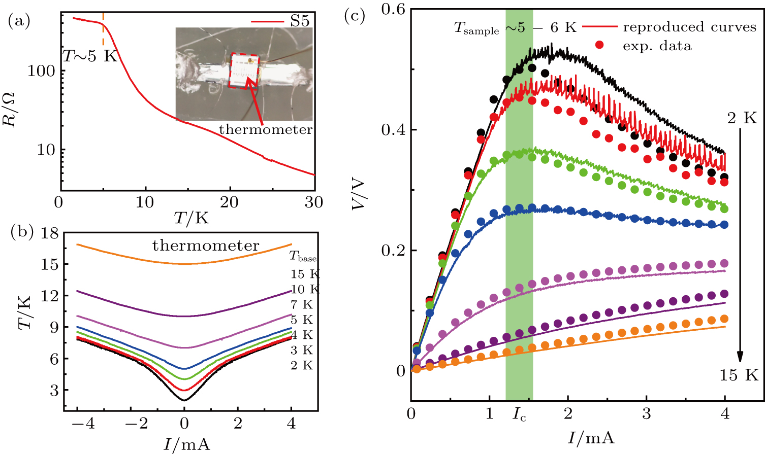
To clarify the underlying physical mechanism of this CC-NDR effect, contributions from Joule-heating effect were studied in detail. A Cernox thermometer was mounted directly on top of the sample using GE-varnish to ensure thermal anchoring and electrical insulation, as the cryostat base temperature cannot represent the real sample temperature when applying large current.[31] Each IV curve was swept slow enough to maximize the thermalization between the sample and the thermometer. By this means, the readings of the thermometer closely represent the sample temperature. In the following, we adopt the thermometer temperature as sample temperature. Figure 3(a) displays the temperature-dependent resistance R(T) of sample 5 and a photograph of the experimental setup is also presented. Both sample 4 and sample 5 show similar behaviors, so here we focus on the sample 5, as it has larger surface and better thermal contact with the thermometer. As shown in Fig. 3(b), the sample temperature measured at various base temperatures T(I) increases monotonically with ramping up bias current. Using the sample R(T) shown in Fig. 3(a) and V = IR relation, these T(I) data can be transferred into corresponding V(I) curves. As shown in Fig. 3(c), the reproduced V(I) results (solid lines) match the direct IV measurements (points) very well. We note that at low temperatures, the calculated V(I) values at large bias current are slightly higher than the measured ones. It is very likely that we underestimated the sample temperature, which overestimates the sample resistance as well as the corresponding voltage. This is due to the existence of certain temperature gradient between the crystal and thermometer, which becomes less significant at higher temperatures. Nevertheless, the reproduced V(I) curves capture the negative differential resistance feature nicely. Moreover, at the critical region where the NDR starts to appear [light green area in Fig. 3(c)], the sample temperature consistently reads out to be 5 K∼ 6 K. It locates exactly at the temperature region above which the sample resistance drops rapidly [see Fig. 3(a)]. These findings strongly indicates that the observed NDR effect in our measurements is closely associated with the intrinsic transition ∼ 5 K of FeSb2, which is, however, mediated by extrinsic current-induced Joule heating effect. Similar NDR effects have also been reported in other systems, which is caused by Joule-heating induced metal-to-insulator transition (MIT).[28,30,31]

Fig. 3. (a) Temperature dependence of the resistance R(T) for sample 5 using the temperature readings recorded by a thermometer attached onto sample surface. Inset: a photograph of the experimental setup. (b) The temperatures recorded on the thermometer as a function of bias current T(I) at various base temperatures. (c) Comparison between the recreated IV curves (lines) using R(T), T(I) shown in panels (a) and (b) and the IV results obtained from direct measurements (points). See the main text for details.
3.3. Magnetic torque measurement of FeSb2 with embedded antimony

As discussed in previous section, saturation of resistivity at low temperature suggests the existence of a conductive state whose origin is unclear yet. These non-trivial transport properties remind us of the well-studied SmB6, in which a topological surface state is possibly realized.[31,34,35] Experimentally, dHvA oscillations have been probed in SmB6 by high precision magnetic torque measurements by Li et al.[35] and Tan et al.[36] The consensus on physical interpretation is, however, not accomplished. Li et al.[35] argued that a two-dimensional metallic surface state with light cyclotron mass (∼ 0.1 me) is responsible for the observed dHvA. In contrast, Tan et al.[36] found that the Fermi surface is three-dimensional and originates from the insulating bulk. Similar quantum oscillations arising from bulk insulating states were also observed both in magneto resistivity and magnetic torque measurements in another Kondo insulator YB12.[37]

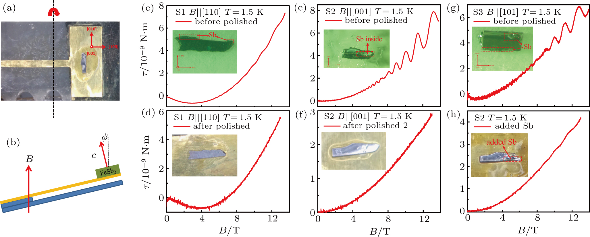
In Fig. 4, we present the magnetic torque measurements on samples where residual antimony flux has not been removed. Details of the experiment setup can be found in Section 2. At a first glance, perfect quantum oscillations are observed in various samples along different crystal orientations as shown in Figs. 4(c), 4(e), and 4(g). The embedded antimony residual is easily detected by EDS inspection [see the insets of Figs. 4(c), 4(e), and 4(g)]. After minimizing antimony contaminations by proper polishing, the aforementioned oscillations are no longer visible at our experimental resolutions [see Figs. 4(d) and 4(f)]. The oscillations are recovered when small amount of antimony is manually added onto the polished crystal (see Fig. 4(h)). Note that the magnitude of the quantum oscillations is rather small (∼ 10−9 N·m), which is comparable to paramagnetic signal of FeSb2. Therefore, the observed dHvA signals in Sb-embedded FeSb2 crystals stem from the crystalline antimony. Recent magnetic torque study on flux-grown SmB6 with embedded aluminum also found a similar quantum oscillations.[38] However, possible existence of non-trivial states cannot be completely ruled out for FeSb2.

Fig. 4. (a) and (b) Optical photograph and a schematic setup of our magnetic torque measurement. (c)–(g) Torque measurements for three as-grown FeSb2 samples (S1–S3) with field applied along different crystal axes, in which nice dHvA oscillations can be seen. Insets: Photographs of crystals clearly show some remaining antimony flux on sample surface. (d) and (f) The same measurements as panels (c) and (e) for S1 and S2 after removing antimony flux by proper polishing, which cannot resolve any oscillations at our experimental resolutions. (h) Recovery of dHvA oscillations by adding some antimony manually onto the polished S2 sample surface. Note: S2 has been polished for two times — After the first polishing, the antimony is seen and checked by EDS, and the dHvA oscillations are observed. After the second polishing, there are no remaining antimony and dHvA oscillations.

We performed quantitative analysis on the observed quantum oscillations using temperature and angular-dependent torque measurements. In Fig. 5(a), the temperature-dependent amplitudes of the dHvA oscillations of S2 (polished 1) are obtained after subtracting a polynomial back ground. It follows the Lifshitz–Kosevich formula,[39,40]

where A = 2π2kBme/e ∼ 14.69 T/K with kB and me being the Boltzmann constant and free electron mass, and is the cyclotron mass. Using fast Fourier transform (FFT) of the quantum oscillations, two or three major frequencies marked as α, α′, and β located between 60 T and 120 T appear clearly [Fig. 5(d) upper slot and inset]. Indeed, these frequencies are quite similar to those found in antimony.[41] As shown in Fig. 5(d), a typical FFT result of FeSb2 (α = 68.9 T and α′ = 82.0 T, upper graph), is quite close to the FFT result of antimony (α = 63.5 T, α′ = 95.7 T, bottom graph). Using Eq. (2), effective cyclotron masses are evaluated for α pocket along B ∥ [001] and B ∥ [100] directions as 0.133 me and 0.094 me, respectively. The estimated effective masses agree well with those of antimony 0.069 me ∼ 0.18 me,[41] depending on different field orientations.

Fig. 5. (a) Amplitudes of the dHvA oscillations at different temperatures after subtracting a polynomial background. (b) Theoretical analysis according to Lifshitz–Kosevich formulation of the dHvA amplitudes for α pocket with field applied along two different directions, which gives a cyclotron mass ∼ 0.1me. (c) Angular dependences [schematic diagram seen in Fig. 4(a) and 4(b)] of the three main frequencies in FFT analysis. The solid lines are the data of the rotation from trigonal axis to bisectrix axis taken from Ref. [41]. The dashed line is a guiding line of the inverse cosine function. (d) The comparison of the scaled frequency spectra between S2 polished 1 (containing embedded Sb) and S2 polished 2 (no Sb) with added Sb.

In Fig. 5(c), we directly compare the angular dependencies of the FFT frequencies of our sample (points) to those of single crystalline Sb (solid lines) reported in Ref. [41]. Nice agreement between α branches is clearly seen although large discrepancies exist between β branches as the remaining Sb flux is poorly crystalized in our sample. Nonetheless, such a qualitative comparison implies that the trapped antimony impurities are somehow crystalized locally and provides strong evidence that the oscillations observed in our FeSb2 system are caused by the remaining antimony. Guiding lines of cosine function, F0/cos(θϕ0), are also shown for comparison, offering description of the angular dependence roughly and suggesting the elongated ellipsoidal Fermi pocket of embedded antimony as the long/short axis ratio is larger than six.[41] We have also carefully compared the electrical transport data before and after polishing, and significant differences are not found. It is reasonable as the portion of the antimony flux is negligible compared to FeSb2 bulk crystal. But our sensitive torque measurements are able to pick up their contributions.

4. Conclusions

In conclusion, we have systematically investigated the electrical transport and magnetization properties on FeSb2 single crystals. Band gaps and carrier information were obtained using the Arrhenius plot and two-carrier model analysis. Current-induced negative differential resistance (CC-NDR) observed at low temperatures is associated with the non-trivial transition ∼ 5 K, which is triggered by current-induced Joule heating effect. The switching effect could play an important role in technological applications and provide a platform for the phase-space analysis in chaotic system. We found clear dHvA oscillations in torque experiments for our FeSb2 but may arise from antimony contaminations. More detailed theoretical and experimental studies are desired to investigate possible non-trivial states in this interesting system. We also anticipate this work of providing a new platform for physical studies and potential applications of Kondo insulator.

Reference
[1] Bentien A Johnsen S Madsen G K H Iversen B B Steglich F 2007 Europhys. Lett. 80 17008
[2] Takahashi H Okazaki R Ishiwata S Taniguchi H Okutani A Hagiwara M Terasaki I 2016 Nat. Commun. 7 12732
[3] Dzero M Sun K Galitski V Coleman P 2010 Phys. Rev. Lett. 104 106408
[4] Fisk Z Sarrao J L Thompson J D Mandrus D Hundley M F Miglori A Bucher B Schlesinger Z Aeppli G Bucher E DiTusa J F Oglesby C S Ott H R Canfield P C Brown S E 1995 Physica B: Condens. Matter 206�?07 798
[5] Kasaya M Iga F Takigawa M Kasuya T 1985 J. Magn. Magn. Mater. 47�?8 429
[6] Hundley M F Canfield P C Thompson J D Fisk Z Lawrence J M 1990 Phys. Rev. 42 6842
[7] Appli G Fisk Z 1992 Comments Condens. Matter Phys. 16 155
[8] Schlesinger Z Fisk Z Zhang H T Maple M B DiTusa J Aeppli G 1993 Phys. Rev. Lett. 71 1748
[9] Fang Y Ran S Xie W Wang S Meng Y S Maple M B 2018 Proc. Natl. Acad. Sci. 115 8558
[10] Nishino Y Kato M Asano S Soda K Hayasaki M Mizutani U 1997 Phys. Rev. Lett. 79 1909
[11] Petrovic C Kim J W Bud’ko S L Goldman A I Canfield P C Choe W Miller G J 2003 Phys. Rev. 67 155205
[12] Petrovic C Lee Y Vogt T Lazarov N Bud’ko S Canfield P 2005 Phys. Rev. 72 045103
[13] Perucchi A Degiorgi L Hu R Petrovic C Mitrović V F 2006 Eur. Phys. J. 54 175
[14] Lukoyanov A V Mazurenko V V Anisimov V I Sigrist M Rice T M 2006 Eur. Phys. J. 53 205
[15] Takahashi H Okazaki R Yasui Y Terasaki I 2011 Phys. Rev. 84 205215
[16] Duong A T Rhim S H Shin Y Nguyen V Q Cho S 2015 Appl. Phys. Lett. 106 032106
[17] Jie Q Hu R Bozin E Llobet A Zaliznyak I Petrovic C Li Q 2012 Phys. Rev. 86 115121
[18] Hu R Thomas K J Lee Y Vogt T Choi E S Mitrović V F Hermann R P Grandjean F Canfield P C Kim J W Goldman A I Petrovic C 2008 Phys. Rev. 77 085212
[19] Bentien A Madsen G K H Johnsen S Iversen B B 2006 Phys. Rev. 74 205105
[20] Tomczak J M Haule K Miyake T Georges A Kotliar G 2010 Phys. Rev. 82 085104
[21] Battiato M Tomczak J M Zhong Z Held K 2015 Phys. Rev. Lett. 114 236603
[22] Du X Tsai S W Maslov D L Hebard A F 2005 Phys. Rev. Lett. 94 166601
[23] Li C Z Li J G Wang L X Zhang L Zhang J M Yu D Liao Z M 2016 ACS Nano 10 6020
[24] Mani A Janaki J Satya A T Geetha Kumary T Bharathi A 2012 J. Phys. Condens. Matter 24 075601
[25] Kawabata A 1980 Solid State Commun. 34 431
[26] Mani R G Ghenim L Choi J B 1991 Solid State Commun. 79 693
[27] Morris R C Christopher J E Coleman R V 1969 Phys. Rev. 184 565
[28] Kim J Ko C Frenzel A Ramanathan S Hoffman J E 2010 Appl. Phys. Lett. 96 213106
[29] Pickett M D Borghetti J Yang J J Medeiros-Ribeiro G Williams R S 2011 Adv. Mater. 23 1730
[30] Chudnovskii F A Odynets L L Pergament A L Stefanovich G B 1996 J. Solid State Chem. 122 95
[31] Kim D J Grant T Fisk Z 2012 Phys. Rev. Lett. 109 096601
[32] Hanias M Anagnostopoulos A N Kambas K Spyridelis J 1991 Phys. Rev. 43 4135
[33] Hanias M P Anagnostopoulos A N 1993 Phys. Rev. 47 4261
[34] Wolgast S Kurdak Ç Sun K Allen J W Kim D J Fisk Z 2013 Phys. Rev. 88 180405
[35] Li G Xiang Z Yu F Asaba T Lawson B Cai P Tinsman C Berkley A Wolgast S Eo Y S Kim D J Kurdak C Allen J W Sun K Chen X H Wang Y Y Fisk Z Li L 2014 Science 346 1208
[36] Tan B S Hsu Y T Zeng B Hatnean M C Harrison N Zhu Z Hartstein M Kiourlappou M Srivastava A Johannes M D Murphy T P Park J H Balicas L Lonzarich G G Balakrishnan G Sebastian S E 2015 Science 349 287
[37] Xiang Z Kasahara Y Asaba T Lawson B Tinsman C Chen L Sugimoto K Kawaguchi S Sato Y Li G Yao S Chen Y L Iga F Singleton J Matsuda Y Li L 2018 Science 362 65
[38] Thomas S M Ding X Ronning F Zapf V Thompson J D Fisk Z Xia J Rosa P F S 2018 arXiv: 1806.00117
[39] Murakawa H Bahramy M S Tokunaga M Kohama Y Bell C Kaneko Y Nagaosa N Hwang H Y Tokura Y 2013 Science 342 1490
[40] Liu Y Yuan X Zhang C Jin Z Narayan A Luo C Chen Z Yang L Zou J Wu X Sanvito S Xia Z Li L Wang Z Xiu F 2016 Nat. Commun. 7 12516
[41] Windmiller L R 1966 Phys. Rev. 149 472