Project supported by the Science Funds from the Ministry of Science and Technology of China (Grant Nos. 2015CB921104 and 2016YFA0300601), the National Natural Science Foundation of China (Grant Nos. 11674380 and 11874063), the Strategic Priority Research Program of the Chinese Academy of Sciences (Grant Nos. XDB07010300 and XDB28000000), and the Key Research and Development Program of Guangdong Province, China (Grant No. 2018B030326001).
Project supported by the Science Funds from the Ministry of Science and Technology of China (Grant Nos. 2015CB921104 and 2016YFA0300601), the National Natural Science Foundation of China (Grant Nos. 11674380 and 11874063), the Strategic Priority Research Program of the Chinese Academy of Sciences (Grant Nos. XDB07010300 and XDB28000000), and the Key Research and Development Program of Guangdong Province, China (Grant No. 2018B030326001).
† Corresponding author. E-mail:
Project supported by the Science Funds from the Ministry of Science and Technology of China (Grant Nos. 2015CB921104 and 2016YFA0300601), the National Natural Science Foundation of China (Grant Nos. 11674380 and 11874063), the Strategic Priority Research Program of the Chinese Academy of Sciences (Grant Nos. XDB07010300 and XDB28000000), and the Key Research and Development Program of Guangdong Province, China (Grant No. 2018B030326001).
We report a fabrication process and characterization of the Josephson parametric amplifier (JPA) for the single-shot quantum state measurement of superconducting multiqubit system. The device is prepared using Nb film as its base layer, which is convenient in the sample patterning process like e-beam lithography and film etching. Our results show that the JPA has a bandwidth up to 600 MHz with gain above 15 dB and noise temperature approaching the quantum limit. The qubit state differentiation measurements demonstrate the signal-to-noise ratio around 3 and the readout fidelity above 97% and 91% for the ground and first-excited states, respectively.
The past years have witnessed a continuous and stimulating progress in the study of superconducting quantum computing and quantum simulation in which the number of quantum bit (qubit) on a chip is increasing.[1,2] In the multiqubit architecture, an amplifier with wide bandwidth is necessary to enable simultaneous readout of the quantum states of multiple qubits with single-shot sensitivity in the low-power dispersive measurement via superconducting microwave resonators coupled to the qubits.[3,4] Josephson parametric amplifiers (JPAs)[5] are often used as such device before the high electron mobility transistor (HEMT) amplifiers, which usually have noise temperature of 2 K–5 K in qubit working range, more than 10–40 times of single photon energy in the readout transmission line.[6] Single-shot readout of the superconducting qubit states has been realized using JPAs of both the narrowband and broadband versions having bandwidths of a few tens[7–9] and a few hundreds[9–11] of MHz, respectively.
The operation of a JPA is based on the principle that the incoming signal photons are mixed with an applied pump tone via intrinsic nonlinearity of Josephson junctions, by which energy from the pump is converted into signal photons, thus providing an effective gain. To increase the amplification bandwidth of the JPA from narrowband to broadband, a common practice is to insert an impedance transformer between the narrowband JPA and the circulator (50-Ω environment) via which the signal to be measured comes to the JPA, and is amplified and reflected out to the HEMT for further amplification. There are two versions of the impedance transformer: One is the combined λ/4 and λ/2 transformer,[10] the other is to use a tapered impedance transformer formed by a long co-planar waveguide (CPW) covered by density-varied crossovers.[11] The latter, which is usually called impedance-transformed parametric amplifier (IMPA), has been used and reported in many studies.[12–16]
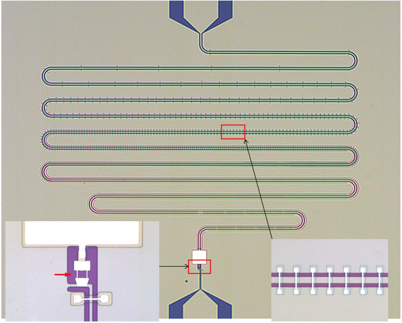
In this work, we present a study of IMPA and develop a fabrication process that is convenient and efficient for the device preparation. We use the Nb film for the bottom layer which contains the CPW and part of lumped-element style superconducting quantum interference device (SQUID) loop and shunt capacitor, as well as the SQUID bias circuitry. This offers several advantages as compared to the previous works in which Al films are used for the bottom layer.[7–11] The Nb layer is patterned by direct writing by laser and reactive ion etching, followed by thermal evaporation of the CaF2 insulating film and double-angle evaporation of the Josephson junctions.[17,18] The IMPAs are then characterized systematically, which demonstrate a gain above 15 dB with a bandwidth as large as 600 MHz and the noise level approaching the quantum limit, thus the device is suitable for the applications with multiqubit purpose with the qubit number up to thirty expectedly. Finally, the IMPAs are tested with quantum state readout of an Xmon qubit. Our results show that the signal-to-noise ratio (SNR)[8,19] and the qubit state readout fidelity[12] are significantly improved by using the IMPA.
In Fig.
In the present experiment, we used thermally oxidized high resistivity silicon substrates with specific resistance greater than 5000 Ω⋅cm. The substrates had a thickness of 0.45 mm with the oxidized layer thickness around 500 nm. The substrates were cleaned sequentially in an ultrasonic bath using acetone and isopropyl alcohol. They were treated at the temperature of 100 °C for 2 hours before being sent into an ultra high vacuum system for Nb film sputtering. The sputter system had a background pressure of 2 × 10⁻⁶ Pa, and Ar gas with purity > 0.9999 and working pressure of 1.5 Pa were used for sputtering. The substrate holder was water cooled so that the sample temperature was kept below 100 °C during sputtering. The sputtering voltage and current were 260 V and 0.45 A, respectively, which gave rise to a film deposition rate of 2.7 nm/s. We used 150-nm thick Nb film for the device bottom layer. The film was then photolithographically patterned using S-1813 resist (1300 nm in thickness) and direct writing by laser (DWL), and dry etched via reactive ion etching (RIE) in SF6, which could be easily controlled compared to the Al film patterning used previously. Subsequently, the resist was removed in acetone and also in a microwave plasma system for the further cleaning of the residuals.
We used thermally evaporated CaF2 film for the insulating layer in the IMPA, which could be conveniently patterned via the lift-off technique, instead of the α-Si film prepared by plasma enhanced chemical vapor deposition.[20] For this we prepared LOR2A/S-1813 (200 nm + 1300 nm) resist double layer. A 200-nm thick LOR2A layer was first spin coated and baked up at 170 °C for 1 minute. A 1300-nm thick S-1813 layer was coated afterward and baked up at 115 °C for 1 minute. The double layer was exposed in the DWL system with the power of 60 W. It was developed at 24 °C for 75 s and fixed for 30 s. Then a 130-nm thick CaF2 film was evaporated in a thermal evaporation system and lifted off, which completed the insulating layer for the capacitor and crossover, etc. The Al layer for the top electrode of the capacitor and crossovers were fabricated subsequently using the lift-off process with single S-1813 resist layer patterned via DWL.
In the final step, shadow evaporated Josephson junctions for the SQUID were prepared in a Plassys system (Plasyss 520) to complete the fabrication of IMPA. Similar conditions to those in our previous work[18] were used for the MAA/PMMA double resist layer preparation for the lift-off process and a pre-cleaning in O2/Ar mixing gases was performed. Different from other reported works, we used the Nb film for the base layer so it was not required to prepare in a separate step the Au film position marks for the e-beam lithography,[9,18] which therefore simplified the sample fabrication process. The Nb film also had better mechanical strength which allowed for repeated bonding of the device in the sample box if required.
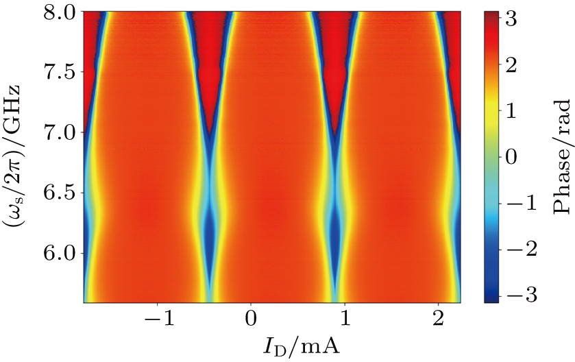
Below we present our experimental results of the fabricated IMPA, which can be roughly divided into two parts: Characterization of the device to find its optimized working parameters and test of the signal amplification with a qubit. As is shown in Fig.
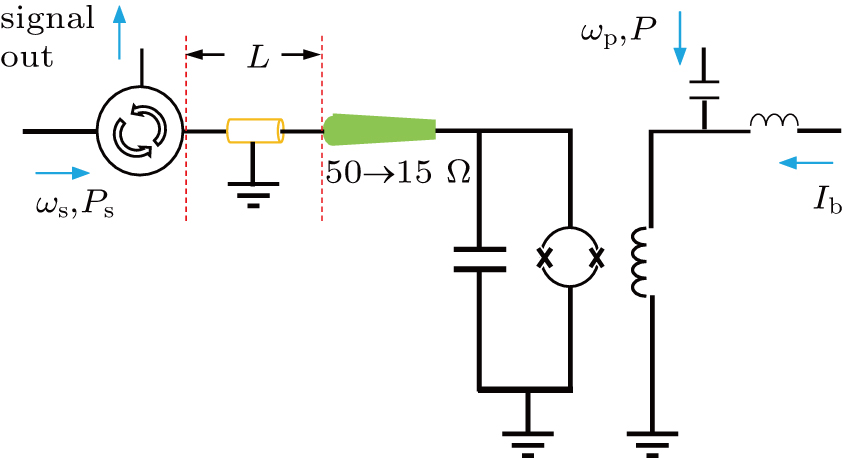
For the measurement of the IMPA, the device was bonded in a copper sample box which was mounted in a cryogen-free dilution refrigerator with standard electronic circuitry for the dispersive readout of transmon or Xmon qubits. The IMPA was connected to the qubit readout transmission line via a circulator as shown on the left side in Fig.
To optimize the working parameters of IMPA we start with the measurement of the gain when an input signal is sent to the qubit readout transmission line which is connected to the signal port on the left side in Fig.
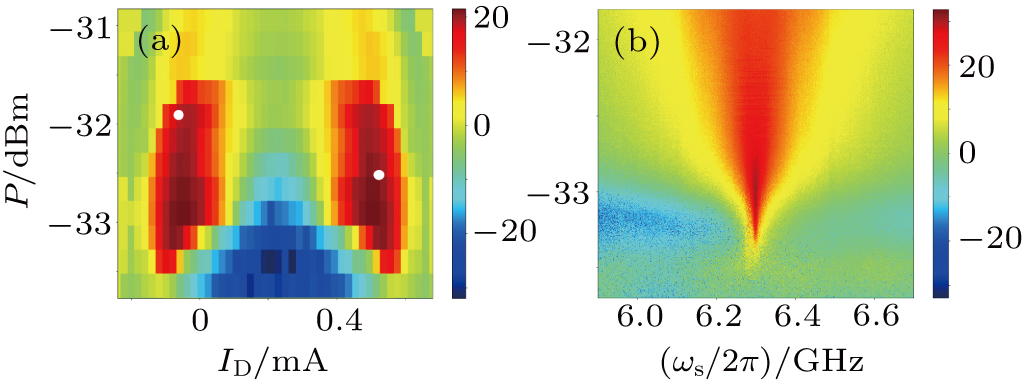
We first set Ib = −0.055 mA and measure the gain under the variations of the pumping power P and the signal frequency ωs/2π with the other parameters unchanged. The result is plotted in Fig.
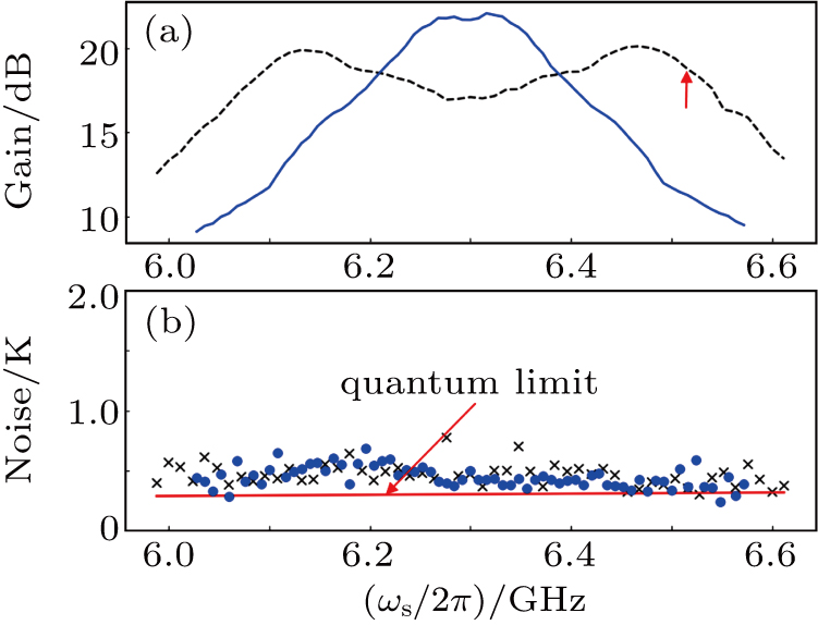
In Fig.
A wider bandwidth of nearly 600 MHz over which the gain is above 15 dB is also achieved, as shown in Fig.
So far the measurements are performed with a fixed signal power of Ps = −116 dBm. By changing Ps and using the parameters in the above experiment, we measure the gain and noise temperature against Ps from −95 dBm down to −135 dBm. It is found that for the gain around 18 dB it basically remains unchanged from −135 dBm up to −115 dBm and starts decreasing noticeably at about −110 dBm. If we define the saturation power as the 1-dB compression point in gain versus the signal power,[7] our results indicate that the saturation power of the present IMPA is around −110 dBm, hence there exists a wide signal power range of the IMPA for the qubit quantum state measurement.
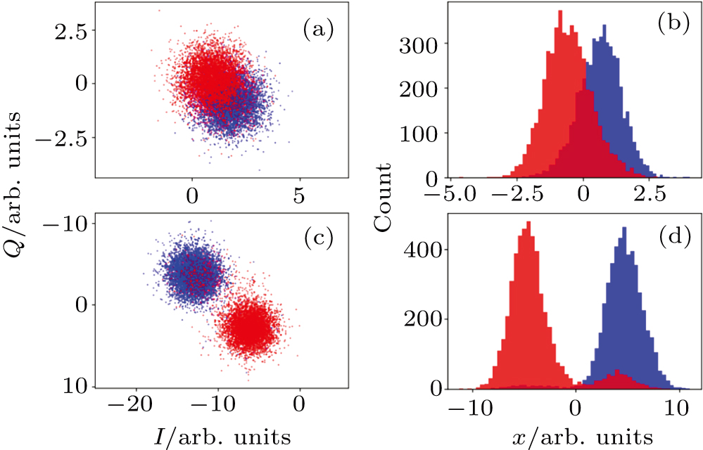
To test the performance of the IMPA, we use an Xmon qubit in an array of 10 coupled qubits with the |0〉 and |1〉 states level spacing of ω10/2π = 4.701 GHz. The qubit has a T1 ranging from 15 μs to 20 μs and a Tφ around 2 μs from the Ramsey interference measurement. The readout resonator has a frequency ωr/2π = 6.515 GHz, a photon decay rate κ/2π = 628 kHz, and the frequency shift parameter χ/2π = 500 kHz that leads to a coupling strength of g/2π = 30 MHz with the qubit. The working parameters for the IMPA are those used in obtaining the result represented by the dashed line in Fig.
In Fig.
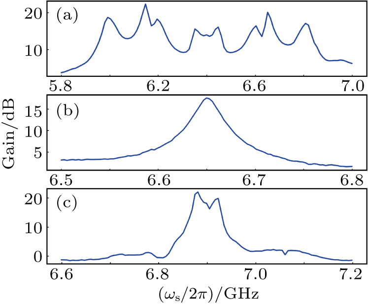
Finally we mention that the above measurements are performed with sample box containing the IMPA connected directly onto the circulator, namely we have L = 0 (see Fig.
We have developed a fabrication process of the IMPA for the quantum state measurement in superconducting multiqubit applications. The process employed Nb film as the base layer, which proved convenient in sample patterning using e-beam lithography and dry etching. The Nb film also had good mechanical strength which allowed for repeated bonding of the device in the sample box. We then presented a systematic characterization of the IMPA. We showed that the JPA had a bandwidth up to 600 MHz with gain above 15 dB and noise temperature approaching the quantum limit. The qubit state differentiation measurements demonstrated an SNR increase by a factor of four and above when pumping of the IMPA was off and on, and the readout fidelity was found to rise to above 97% and 91% for the ground and first-excited states, respectively. The present IMPA can be used for the single-shot quantum state measurement of the multiqubit system with the qubit number up to around thirty.
| [1] | |
| [2] | |
| [3] | |
| [4] | |
| [5] | |
| [6] | |
| [7] | |
| [8] | |
| [9] | |
| [10] | |
| [11] | |
| [12] | |
| [13] | |
| [14] | |
| [15] | |
| [16] | |
| [17] | |
| [18] | |
| [19] | |
| [20] |


