Photovoltaic effects in reconfigurable heterostructured black phosphorus transistors
Hu Siqi1, Tian Ruijuan1, Luo Xiaoguang2, Yin Rui1, Cheng Yingchun2, Zhao Jianlin1, Wang Xiaomu3, Gan Xuetao1, †
MOE Key Laboratory of Material Physics and Chemistry under Extraordinary Conditions, and Shaanxi Key Laboratory of Optical Information Technology, School of Science, Northwestern Polytechnical Univeristy, Xi’an 710072, China
Shannxi Institute of Flexible Electronics, Northwestern Polytechnical University, Xi’an 710072, China
School of Electronic Science and Engineering, Nanjing University, Nanjing 210023, China


† Corresponding author. E-mail: xuetaogan@nwpu.edu.cn

Project supported by the National Key Research and Development Program of China (Grant Nos. 2018YFA0307200 and 2017YFA0303800), the National Natural Science Foundations of China (Grant Nos. 61522507 and 61775183), the Key Research and Development Program in Shaanxi Province of China (Grant No. 2017KJXX-12), and the Fundamental Research Funds for the Central Universities (Grant Nos. 3102017jc01001 and 3102018jcc034).

Abstract

We demonstrate a reconfigurable black phosphorus electrical field transistor, which is van der Waals heterostructured with few-layer graphene and hexagonal boron nitride flakes. Varied homojunctions could be realized by controlling both source–drain and top-gate voltages. With the spatially resolved scanning photocurrent microscopy technique, photovoltaic photocurrents originated from the band-bending regions are observed, confirming nine different configurations for each set of fixed voltages. In addition, as a phototransistor, high responsivity (∼ 800 mA/W) and fast response speed (∼ 230 μs) are obtained from the device. The reconfigurable van der Waals heterostructured transistors may offer a promising structure towards electrically tunable black phosphorus-based optoelectronic devices.

1. Introduction

Two-dimensional (2D) materials rose sharply after the exfoliation of graphene in 2004.[13] A large number of 2D materials ranging from semimetal to semiconductor and to insulator have been investigated,[46] and some of them are considered as promising next-generation constituents in optoelectronic circuitry.[79] Graphene was once a good choice for optoelectronic applications due to the broad band absorption and high carrier mobility (in the order of 104 cm2·V–1·s-1). However, the absence of bandgap makes graphene only a good 2D electrode due to the low absorbance and bad current on/off ratio. For a single device such as a field-effect transistor (FET), the high mobility channel materials with moderate bandgap are desired.

Black phosphorus (BP) with a monolayer thickness of ∼ 0.53 nm recently emerges as a good candidate for 2D material-based optoelectronics.[10] Its direct bandgap could be varied from 0.3 eV to 1.3 eV by reducing the layer number to monolayer gradually.[11] This bandgap leads to a very good current on/off ratios (up to 105) in the FET, which is superior to the gapless graphene. The carrier mobility of few-layer BP, in the order of 102 cm2·V–1·s–1 at room temperature,[12] is higher than those in most of the 2D semiconductors, such as transition-metal dichalcogenides. In addition, BP’s ambipolarity promises it to be a good channel material for constructing electrostatically tuned optoelectronic devices.[1117] The limitation for BP devices is mainly the bad air-stability, which fortunately could be overcome from encapsulation by other transparent insulators.[18] Hexagonal boron nitride (h-BN) is such a 2D insulator with a large bandgap (> 5 eV), which is also suitable as a gate dielectric material.[4,6,19] Combining 2D materials with different electronic properties ranging from semimetal e.g., graphene) to semiconducting e.g., BP) and to insulating e.g., h-BN), one could fabricate various electronic and optoelectronic devices by simple van der Waals contact with flat surfaces and disorder-free interfaces.

Here, we present the achievement of a reconfigurable BP FET, which is van der Waals heterostructured with graphene and h-BN. A few-layer BP channel is in contact with source-drain graphene electrodes and covered by a top h-BN dielectric layer. Another graphene sheet on the top of h-BN acts as the top-gate electrode. Nine different configurations of the homojunction over the BP channel are achieved by controlling both the drain-source voltages and gate voltages. The applied voltages are less than 2 V. All configurations can be spatially visualized and confirmed by scanning photocurrent microscopy (SPCM). Meanwhile, the phototransistor has a high responsivity (up to 800 mA/W) and a fast response speed (∼ 230 μs), offering potential applications towards photodetection and energy harvesting based on few-layer BP.

2. Fabrication and characterization of BP devices

Figure 1(a) shows the cross-section schematics of a BP-based top-gate FET on an SiO2/Si substrate. Two prepatterned graphene sheets underneath the BP flake act as source and drain electrodes, sandwiched by two transferred h-BN flakes which perform as a substrate and a top-gate dielectric, respectively. The double-deck h-BN flakes also encapsulate BP flake to refrain it from degeneration. Another prepatterned graphene sheet was finally stamped above the BP channel region as the top-gate. To fabricate the device, graphene, BP and h-BN layers are mechanically cleaved from their bulk materials onto polydimethylsiloxane (PDMS) stamps,[20] which facilitates the precise alignment and transfer of the 2D flakes into the proposed heterostructures. An optical microscopic image of the finished device is shown in Fig. 1(b). To confirm the quality of the BP layer, Raman spectra are acquired from the device with the excitation of 532-nm laser. As shown in Fig. 1(c), characteristic , B2g, and peaks are clearly observed at the wave-number of 363.3 cm–1, 440.4 cm–1, and 469.2 cm–1. Atomic force microscopy (AFM) technique is employed to examine the thicknesses of the 2D flakes. Figure 1(d) shows the AFM image of the area denoted by the black dashed box of Fig. 1(b), indicating thicknesses of BP and top h-BN are about 8 nm (15 layers) and 12 nm, respectively.

Fig. 1. (color online) BP FET based on van der Waals heterojunctions. (a) Cross-section schematics of a BP FET with all 2D constituents on SiO2/Si substrate. The three-terminal measurement scheme is also shown. (b) Optical image of the device. The scale bar is 20 μm. (c) Raman spectra of BP flakes. (d) Atomic force microscopy image of the BP FET inside the dotted black box shown in panel (b). BP thickness is 8 nm and h-BNT thickness is 12 nm. The scale bar is 5 μm.
3. Results and discussion
3.1. Reconfigurable operation of BP devices

A typical electrical transfer characteristic of the fabricated BP top-gate transistor is shown in Fig. 2(a), where the source-drain voltage is Vds = 10 mV. A transport gap of ΔVg ∼ 0.38 V is observed around Vg = 0 V, which is extracted from the linear extrapolation of Ids. Subsequently, the band gap of BP can be estimated by the change of Fermi level (or chemical potential) EF upon the transport gap,[21] where Δ ϕ = e2n/CG counts the variation in the electrostatic potential with the electron charge e, the carrier density n and the geometrical capacitance CG. The carrier density in BP film can be estimated as n = (Δ VgCG)/e and the geometrical capacitance of top h-BN is CG = (εh–BN)/hh–BN, with εh–BN = 4.2ε (vacuum permittivity ε ) the relative dielectric constant[4] of top h-BN and the thickness hh–BN = 12 nm, respectively. We then estimate that CG = 309.8 nF/cm–2 and the band gap of the 15 layers BP film is ΔEF = 0.32 eV, which is close to the bulk band gap of ∼ 0.3 eV.[22] It is known that the values of the electron affinity and the ionization potential relative to the vacuum of few-layer BP film are about 4.1 eV and 4.4 eV,[23] respectively, and thus the graphene Fermi energy (4.5 eV) is 0.1 eV lower than the top of the valence band of BP film from the band alignment. As a result, the band in BP film bends downward to the bottom graphene layer with a build-in field, and the device is intrinsic with slight p-type carriers. This is confirmed from the asymmetric transfer IdsVg curve around Vg= 0 V, as shown in Fig. 2(a).

Fig. 2. (color online) Characteristics of the BP FET. (a) Electrical transfer characteristic (IdsVg curve) at Vds = 10 mV. (b) Semi-log plots of output characteristics (|Ids|–Vds curves) at various Vg values from –2 V to 2 V with a 1-V step. Inset: the corresponding linear plots. (c) and (d) Semi-log plots of electrical transfer characteristics for (c) negative and (d) positive Vds.

Figure 2(b) shows the output characteristics in semi-log and linear (inset) scales for Vg from –2 V to 2 V in the step of 1 V. The diode-like current rectifications were observed for all Vg’s except that around 0 V. The Vg-dependent rectification behaviors could be modulated from the rectification directionalities, the polarities, and their degrees. For example, a positive forward current flows at positive Vds when Vg = –1 V, while the direction of current is reversed when Vg = 1 V. From the electrical transfer characteristics (|Ids|–Vg curves) versus different Vds shown in Figs. 2(c) and 2(d), the ambipolarity at low Vds is modulated to electron- or hole-dominant polarity as Vds increases from –2 V to 2 V. Minimum subthreshold swing S = dVg/(d ln Ids) ∼ 340 mV/dec is observed at low source-drain voltage |Vds| = 0.1 V. Besides, the measured Schottky barrier height between gold electrode and graphene (not shown here) is much smaller than that in the graphene-BP junction in our devices, thus we eliminate the influence of the Schottky junction. So far, tunable diode characteristics or polarities have been achieved in our device by adjusting Vds and Vg, which are in the same voltage scale. In other words, our device can be reconfigured by a specified set of Vds and Vg values.

The asymmetric property of Fig. 2(a) also implies the slight band bending at Vg = 0 V and Vds = 0 V, where the Fermi energy is estimated to be a little lower than the mid-gap of BP film. Considering the weak photoresponse at low applied voltages from our following experimental results, we still regard this slight p-type as i (intrinsic) type. Figure 3 shows the band diagram configurations for each set of Vds and Vg, corresponding to those arrows in the device characteristics of Figs. 2(b), 2(c), and 2(d). The equilibrium state when Vg = 0 V and Vds = 0 V is shown in Fig. 3(a), which is regarded as an overall i type due to the nearly flat band configuration. To distinguish the reconfigurations of the device, the sign and magnitude of Vg,eff(x) = VgV(x) are adopted to determine the carrier type (n type, i type, or p type) and carrier density, which is the effective gate field along the channel and V(x) is the channel voltage. For the green curve of Fig. 2(b), when Vds varies from –2 V to 1 V and to 2 V at the fixed Vg= 1 V, the corresponding channel voltage along the channel (from left to right) can be expressed as [–2 V, 0 V], [1 V, 0 V], and [2 V, 0 V] respectively after assuming a constant voltage drop along the channel for simplicity. Then one can find the corresponding effective gate field as [3 V, 1 V], [0 V, 1 V], and [–1 V, 1 V], leading to n type, i–n type, and p–i–n type configurations, as shown in turn in Figs. 3(b)3(d). The energy barriers formed at the contacts are asymmetric in these reconfigurations, resulting in asymmetric injection of dominant carriers, and finally realizing channel conductance. In the same way, when Vg varies from –2 V to –1 V, 0 V, and 2 V at the fixed Vds = –2 V (i.e., the arrows in the black curve of Fig. 2(c)), the corresponding band structures can be assigned to i–p, n–i–p, n–i, and n, respectively, as shown in turn in Figs. 3(e)3(h). At the fixed Vds = 2 V, Vg varies from –2 V to 0 V, 1 V, and 2 V (i.e., the arrows in the black curve of Fig. 2(d)) corresponds to p, p–i, p–i–n, and i–n, respectively, as shown in turn in Figs. 3(i)3(l). Therefore, nine different configurations (Fig. 3) from a single device can be achieved for each set of Vds and Vg, which will be confirmed by the spatially resolved SPCM technique in the following.

Fig. 3. (color online) Band diagrams for reconfigurable device operations. (a) Schematic band diagram of a BP FET with all 2D components at equilibrium (Vds = Vg = 0 V). (b)–(d) Band configurations for the |Ids|–Vds characteristic, following the arrows in the green curve shown in Fig. 2(b). (e)–(h) Band configurations for the |Ids|–Vg characteristics following the arrows in the black curve shown in Fig. 2(c). (i)–(l) Band configurations for the |Ids|–Vg characteristics following the arrows in the black curve shown in Fig. 2(d).
3.2. Photovoltaic effect in reconfigurable heterostructured BP devices

In the fabricated heterostructued BP device, photocurrent would generate at the band bending region via the photovoltaic effect. The spatially resolved SPCM technique is therefore a good way to visualize the device configuration. Figure 4(a) shows scanning photocurrent maps of the BP FET at different set of (Vds, Vg), where the black dashed lines indicate the underlying graphene source and drain electrodes, the black full line denotes the graphene top-gate electrode, and the white dashed line represents the BP film. We chose the 532-nm laser for photoelectric measurements, because the 532-nm laser is visible in both microscope and visible-light CCD, which is convenient to determine the measuring location of the devices. During the scanning, a laser with the spot diameter of ∼ 3 μm is focused on the device, whose wavelength and power are 532 nm and 25 μW, respectively. The current flowing from left to right are defined as positive. Then we observe nine different visual maps with photocurrent in the color scale, as shown in Fig. 4(a). It is noted that the photocurrent mainly comes from the contact regions between BP and the graphene, which implies that band bending happens at the contacts. Nine photocurrent maps are distinguished from each other by the different photocurrent distribution of the contacts.

Fig. 4. (color online) Reconfigurable SPCM with band diagrams. (a) SPCM maps of the BP FET with color scale for nine different configurations. The sets of (Vds, Vg) for each configuration in turn are: (–2 V, –2 V), (–2 V, –1 V), (–2 V, 0 V), (0 V, –2 V), (0 V, 0 V), (0 V, 2 V), (2 V, 0 V), (2 V, 1 V), and (2 V, 2 V), respectively. (b) The corresponding schematic band diagrams of SPCM maps.

To explain the photocurrent maps, we draw the simplified band diagram according to the analysis in Fig. 3, as displayed in Fig. 4(b). In equilibrium state, i.e., (0 V, 0 V), few nanoamperes of the photocurrent is observed, which is almost 2 orders less than the current of other nonequilibrium configurations. The reason for this weak photoresponse is because the band bending in this slight p-type configuration is not strong enough to boost the electron–hole separation and finally leads to negligible photocurrent. Generally, the sign of the photocurrent is determined by the slope of the band bending. Taking the case of (–2 V, –1 V) as an example, as shown at the top middle map in Fig. 4(a), negative photocurrents at both contacts are measured, consistent with the n–i–p configuration at the top middle diagram shown in Fig. 4(b). For the one junction case such as the p–i configuration (2 V, 0 V), only a positive photocurrent at the left contact is observed, as shown at the bottom left map in Fig. 4(a), corresponding to a flat-band configuration near the right contact. For the overall p- or n-dominant configurations in the middle left or right diagram shown in Fig. 4(b), we measure the photocurrents with opposite directions at each contact shown in Fig. 4(a). In a word, all nine configurations with the band diagram shown in Fig. 4(b) match the SPCM images shown in Fig. 4(a) very well.

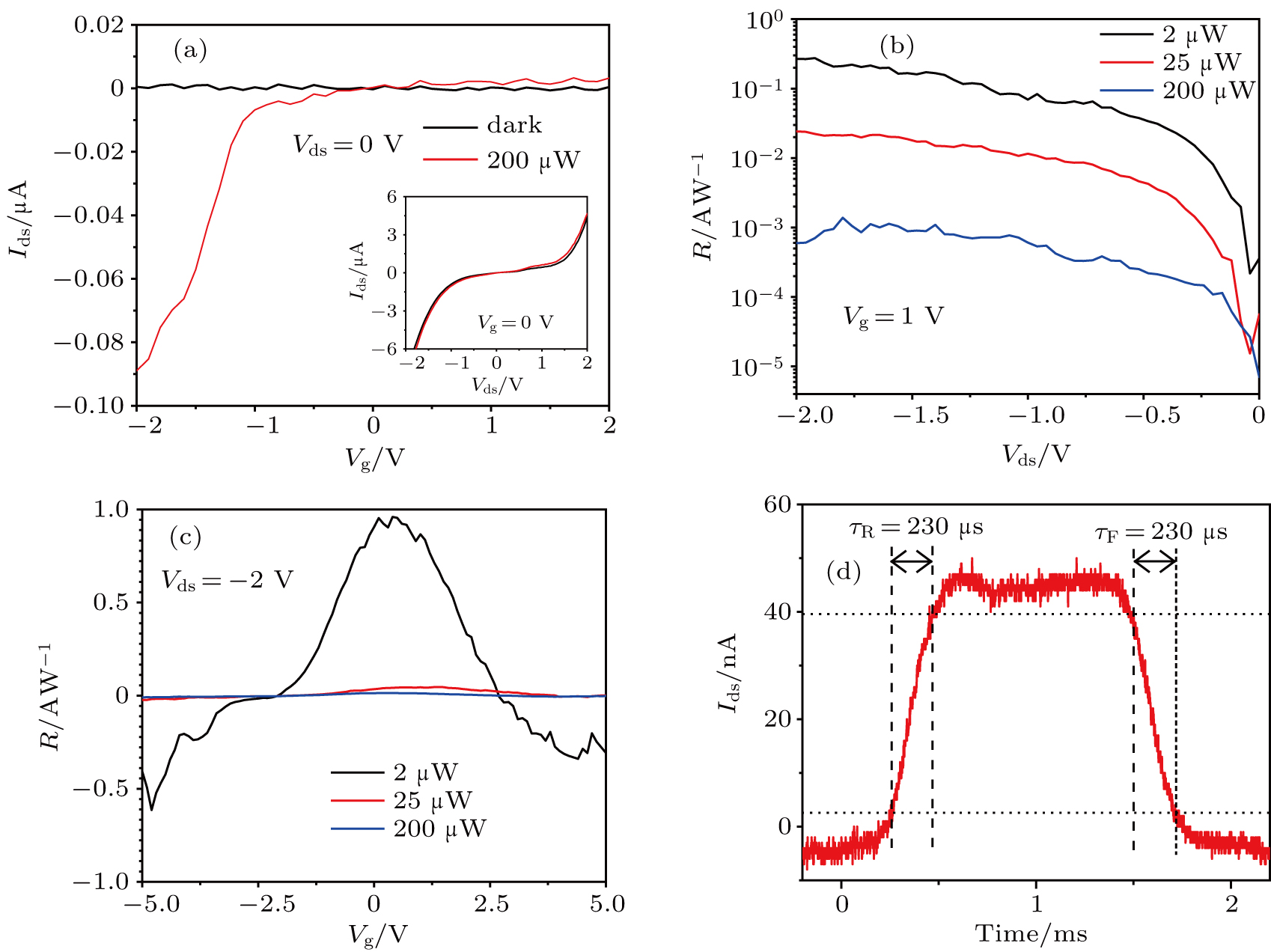
To investigate the photoresponse of our BP-based transistor, photocurrent measurements are carried out at a BP-graphene contact. Figure 5(a) shows Ids versus Vg curves at Vds = 0 V (inset: Ids versus Vds curves at Vg = 0 V) in dark (black line) and under 200- μW laser illumination (red line). An obvious photoresponse is observed except Vg = Vds = 0 V. The negligible photoresponse at Vg = Vds = 0 V directly proves the i-type assumption presented in Fig. 3(a). The responsivity (R) is defined as the photocurrent generated per unit power of incident light,[9] where the photocurrent Iph = IillumIdark and the light intensity P is the laser power due to the small laser spot. From the results of Figs. 5(b)5(c), it is found higher responsivity can be obtained for weaker laser, and a high R up to 800 mA/W is measured at the low power of 2 μW when Vds = –2 V and Vg = 1 V, which dramatically decreases to 0.6 mA/W at 200 μW. The presence of the trap states either in BP or at the interface between BP and other 2D material layers may be responsible for such a reduction in photoresponsivity.[24] This nonlinear response of R is also reported in many 2D or heterostructure devices.[2530] Hence, the poor linear dynamic range needs to be improved for further photodetector application. The external quantum efficiency EQE is estimated as (Iph/P)/(hc/eλ ) = 37.7% at the high value of R, where h and c are Planck’s constant and the speed of light, respectively. In addition, the time response of photocurrent with a chopper is recorded for the p–i configuration (Vds = 2 V, Vg = 0 V), as shown in Fig. 5(d), from which one can find the rise time τR and the fall time τF are both evaluated as 230 μs.

Fig. 5. (color online) Photocurrent measurements of the phototransistor with a 532-nm laser illuminated at one BP-graphene contact region. (a) Ids with respect to Vg at Vds = 0 V in dark (black line) and illumination (red line) at the contact region. The laser power is 200 μW. Inset: Ids versus Vds curves at Vg = 0 V. (b) The responsivity R versus Vds curves when Vg = 1 V and (c) R versus Vg curves when Vds = –2 V with three different laser powers (black: 2 μW, red: 25 μW, blue: 200 μW). (d) Time response measurement of Ids by using a chopper.
4. Summary

In summary, we have fabricated a van der Waals heterostructured top-gate transistor with all 2D constituents (including BP, graphene, and h-BN layers). By applying less than 2 V of both top-gate and source–drain voltages, this device has been reconfigured successfully by utilizing the ambipolar tunable characteristics of BP channel, where nine different configurations have been realized. By spatially resolved scanning photocurrent microscopy technique, all configurations were directly visualized, and the photocurrent was only detected at the contact regions where band bending occurred. In addition, high responsivity and fast photoresponse speed have been observed in the devices, assuring the potential ability in photodetection. Consequently, our reconfigurable heterostructured BP transistors may offer a potential useful structure towards electrically tunable photovoltaic devices.

Reference
[1]Novoselov K S Geim A K Morozov S V Jiang D Katsnelson M I Grigorieva I V Dubonos S V Firsov A A 2005 Nature 438 197
[2]Zhang Y Tan Y W Stormer H L Kim P 2005 Nature 438 201
[3]Novoselov K S Jiang D Schedin F Booth T J Khotkevich V V Morozov S V Geim A K 2005 Proc. Natl. Acad. Sci. USA 102 10451
[4]Dean C R Young A Meric I Lee C Wang L Sorgenfrei S Watanabe K Taniguchi T Kim P Shepard K L Hone J 2010 Nat. Nanotechnol. 5 722
[5]Radisavljevic B Radenovic A Brivio J Giacometti V Kis A 2011 Nat. Nanotechnol. 6 147
[6]Ross J Klement P Jones A M Ghimire N Yan J Mandrus D Taniguchi T Watanable K Kitamura K Yao W Cobden D Xu X 2014 Nat. Nanotechnol. 9 268
[7]Kim K Choi J Kim T Cho S Chung H 2011 Nature 479 338
[8]Novoselov K S Fai Ko V I Colombo L Gellert P R Schwab M G Kim K 2012 Nature 490 192
[9]Koppens F H L Mueller T Avouris Ph Ferrari A C Vitiello M S Polini M 2014 Nat. Nanotechnol. 9 780
[10]Xia F Wang H Jia Y 2014 Nat. Commun. 5 4458
[11]Liu H Neal A T Zhu Z Luo Z Xu X Tomanek D Ye P D 2014 ACS Nano 8 4033
[12]Li L Yu Y Ye G J Ge Q Q Ou X Wu H Feng D L Chen X Zhang Y 2014 Nat. Nanotechnol. 9 372
[13]Qiao J Kong X Hu Z Yang F Ji W 2014 Nat. Commun. 5 4475
[14]Koenig S P Doganov R A Schmidt H Castro Neto A H Özyilmaz B 2014 Appl. Phys. Lett. 104 103106
[15]Buscema M Groenendijk D J Blanter S I Steele G A Van Der Zant H S J Castellanosgomez A 2014 Nano Lett. 14 3347
[16]Dai J Zeng X C 2014 J. Phys. Chem. Lett. 5 1289
[17]Tran V Soklaski R Liang Y Yang L 2014 Phys. Rev. 89 235319
[18]Chen X Wu Y Wu Z Han Y Xu S Wang L Ye W Han T He Y Cai Y Wang N 2015 Nat. Commun. 6 7315
[19]Wang L Meric I Huang P Y Gao Q Gao Y Tran H Taniguchi T Watanabe K Campos L M Muller D A Guo J Kim P Hone J Shep-ard K L Dean C 2013 Science 342 614
[20]Castellanosgomez A Buscema M Molenaar R Singh V Janssen L Van Der Zant H S J Steele G A 2014 2D Mater. 1 011002
[21]Saito Y Iwasa Y 2015 ACS Nano 9 3192
[22]Warschauer D M 1963 J. Appl. Phys. 34 1853
[23]Li D Wang X Zhang Q Zou L Xu X Zhang Z 2015 Adv. Funct. Mater. 25 7360
[24]Kind H Yan H Messer B Law M Yang P 2002 Adv. Mater. 14 158
[25]Lopezsanchez O Lembke D Kayci M Radenovic A Kis A 2013 Nat. Nanotechnol. 8 497
[26]Chen Y Wang X Wu G Wang Z Fang H Lin T Sun S Shen H Hu W Wang J Sun J Meng X Chu J 2018 Small 14 1703293
[27]Liu F Shimotani H Shang H Kanagasekaran T Zolyomi V Drum-mond N Fal Ko V I Tanigaki K 2013 ACS Nano 8 752
[28]Zhang E Jin Y Yuan X Wang W Zhang C Tang L Lou S Zhou P Hu W Xiu F 2015 Adv. Funct. Mater. 25 4076
[29]Wang X Wang P Wang J Hu W Zhou X Guo N Huang H Sun S Shen H Lin T Tang M Liao L Jiang A Q Sun J Meng X Chen X Lu W Chu J 2015 Adv. Mater. 27 6575
[30]Mudd G W Svatek S A Hague L Makarovsky O Kudrynskyi Z R Mellor C J Beton P H Eaves L Novoselov K S Kovalyuk Z D Vdocin E E Marsden A J Wilson Neil R Patane A 2015 Adv. Mater. 27 3760