Total ionizing dose effects in pinned photodiode complementary metal-oxide-semiconductor transistor active pixel sensor
Ma Lin-Dong1, 2, 3, Li Yu-Dong1, 2, Wen Lin1, 2, Feng Jie1, 2, Zhang Xiang1, 2, 3, Wang Tian-Hui1, 2, 3, Cai Yu-Long1, 2, 3, Wang Zhi-Ming1, 2, 3, Guo Qi1, 2, †
Key Laboratory of Functional Materials and Devices for Special Environments of Chinese Academy of Sciences, Xinjiang Technical Institute of Physics & Chemistry, Urumqi 830011, China
Xinjiang Key Laboratory of Electronic Information Material and Device, Urumqi 830011, China
University of Chinese Academy of Sciences, Beijing 100049, China


† Corresponding author. E-mail: guoqi@ms.xjb.ac.cn

Project supported by the National Natural Science Foundation of China (Grant No. 11675259) and the West Light Foundation of the Chinese Academy of Sciences (Grant Nos. 2016-QNXZ-B-8 and 2016-QNXZ-B-2).

Abstract

A pinned photodiode complementary metal–oxide–semiconductor transistor (CMOS) active pixel sensor is exposed to 60Co to evaluate the performance for space applications. The sample is irradiated with a dose rate of 50 rad (SiO2)/s and a total dose of 100 krad (SiO2), and the photodiode is kept unbiased. The degradation of dark current, full well capacity, and quantum efficiency induced by the total ionizing dose damage effect are investigated. It is found that the dark current increases mainly from the shallow trench isolation (STI) surrounding the pinned photodiode. Further results suggests that the decreasing of full well capacity due to the increase in the density, is induced by the total ionizing dose (TID) effect, of the trap interface, which also leads to the degradation of quantum efficiency at shorter wavelengths.

1. Introduction

Complementary metal–oxide–semiconductor transistor (CMOS) active pixel sensors (APSs), due to their low power consumption, high-level integration, and low cost, have reached or even exceeded charge-coupled devices (CCDs) in the performance level.[1,2] Compared with 3 transistor (3T) CMOS APS, a p+ layer is added on the top of the n-layer of a normal photodiode in pinned photodiode (PPD, 4T) CMOS APS, which is used to solve the interline transfer lag problem and thermal noise problem, and reduce the dark current from the surface. Unlike the CCDs, the PPD CMOS APS does not suffer charge transfer degradation. Since PPD CMOS APS is the most promising sensor for high performance imaging applications at a low light level and in an extreme environment (especially for space, scientific, nuclear, medical, and military instruments applications), radiation damage is our primary concern.[3]

The effects of radiations damage on 3T CMOS image sensors have been widely studied.[46] On the contrary, the radiation effects on 4T pixels have not been very well understood yet. There are significant differences among the total dose damage mechanisms of CMOS APS with different pixel structures. The previous studies indicated that gamma irradiation leads the quantum efficiency to increase for 3T APS,[7] while the present work shows that the gamma irradiation can cause the quantum efficiency to decrease for 4T APS.

The aim of this work is to provide an overview of the degradation in 4 T CMOS APS induced by Cobalt60 irradiation. In this paper, we study the main origins of the increase in dark current in a pinned photodiode caused by the total ionizing dose effect at 100 krad (SiO2). Moreover, the degradation mechanisms of full well capacity and quantum efficiency are also analyzed.

2. Experimental details
2.1. Devices information

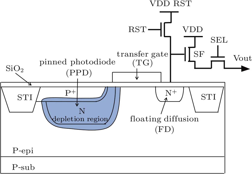
The PPD CMOS APS was a scientific image sensor with 2048 by 2040 pixels, manufactured using 0.18-μm standard CMOS technology. The sensor was operated in rolling shutter mode. Figure 1 shows the schematic of a PPD 4T pixel with the cross-section of the photo-sensing element, a charge transfer gate (TG), and floating diffusion (FD). The gate oxide thickness is 7 nm and the thickness of shallow trench isolation (STI) surrounding the PDD is around 360 nm. As can be seen, the photo-sensing element consists of two p–n junctions: the p+/n junction close to the surface and the n/p-sub junction in the silicon bulk. As shown in the figure, the photo-electrons are generated and collected in the PPD during the exposure time. After that, the FD needs to be reset first to remove any redundant charges. In the end, the TG is switched on so that the electrons stored in the PPD flow to the FD, and are subsequently read-out through a source follower (SF). VOFF is the voltage applied to the TG when the TG is switched off with a nominal 0 V. This region of pixels is considered to be the most vulnerable to the effects of radiation.

Fig. 1. (color online) Schematic diagram of PPD 4T pixel.
2.2. Irradiation conditions

Considering that a sensor has 400 million pixel unites, a sample has been exposed to 60Co gamma ray up to 100 krad (SiO2) at a dose rate of 50 rad (SiO2)/s. During the irradiation, the sensor was unbiased with all pins grounded, and gamma irradiation was performed using 60Co gamma source at the Xinjiang Technical Institute of Physics and Chemistry in Urumqi, China. All parameters were measured immediately after irradiation at room temperature (around 23 °C) in the case of annealing.

2.3. Annealing

In order to discriminate the contributions of the two kinds of defects, trapped oxide charges and interface states, after gamma irradiation, annealing tests at 100 °C and 200 °C for 168 hours were performed, respectively.

3. Results of gamma rays irradiation
3.1. Ionizing effect leading to increase of dark current

The dark signal is defined as the carriers generated in the potential wells under the pixel in fully dark conditions. Figure 2 shows the degradation of the dark current as a function of the total dose. It increases with the TID increasing as expected.

Fig. 2. Variation of dark current with total ionizing dose.

When an APS is irradiated by gamma rays and protons, several mechanisms induce the dark current to increase. Displacement damage produced by gamma rays is negligible, leading to the bulk dark current remaining unchanged. Damages can cause a build-up of traps at the interface (usually called Si/SiO2 interface traps), which induces the current to increase near the depleted region in the photodiode. As a consequence, trapped oxide charges will change the distribution of the electric field and modify the Si/SiO2 interface potential, which can cause the depletion region to extend and thus strongly affecting the generation rate of the charge in the neutral state. The distribution of the origin of dark current in PPD CMOS APS has been proposed in previous work[810] and is shown in Fig. 3. The first source of dark current is that the current comes from the transfer gate where the depletion region is close to the interface, in which the generation of interface states increases the dark current.[8] The second source is that the current comes from the STI surrounding the photodiode as presented in Ref. [9]. The last one, which was presented in Ref. [10], is that at high total dose (i.e., above 300 krad (SiO2)), the dielectric above the pinned-photodiode is involved.

Fig. 3. Dark current generation mechanism after irradiation with γ-ray.

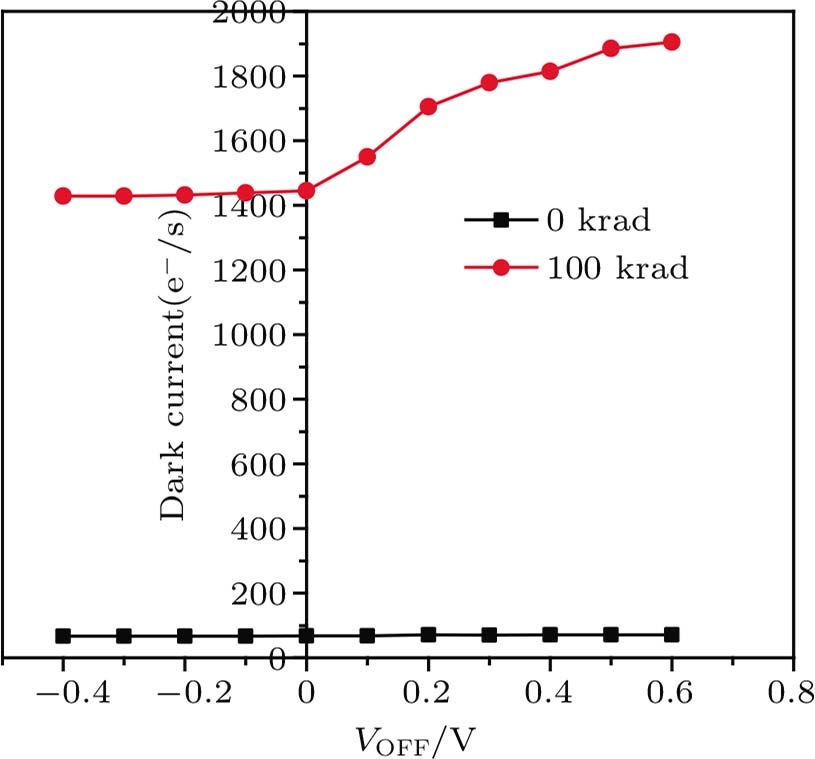
In this paper, we simply distinguish the contributions of the different origins of dark current. We believe that the dark current coming from the dielectric can be ignored after the highest TID only at 100 krad (SiO2). The main sources come from the interface states located at TG and STI, which surround the PPD. The number of dark electrons from the TG edge strongly depends on the bias. When VOFF is set to be at negative bias, the TG is accumulated with holes which recombine with dark electrons generated from interface defects and fill the traps caused by γ -irradiation around the TG.[11] If the dark current generated in the TG is suppressed by using a negative bias, the remaining dark current mainly comes from STI.

As shown in Fig. 4, the dark current shows no evident change under VOFF voltages ranging from −0.4 V to 0 V, while dark current increases sharply for a VOFF higher than 0 V. For non-irradiated sensor, the dark current slightly increases at VOFF above 0 V, indicating that the generation of the interface at the TG with 100 krad (SiO2), the current from the TG is negligible at a VOFF of 0 V, coming mainly from the STI surrounding the photodiode.

Fig. 4. (color online) Variation in dark current with VOFF voltage.
3.2. Ionizing effect leading to decrease of full well capacity

The maximum output voltage swing of an image sensor can be limited either by the saturation of the readout circuit or by the full well capacity (FWC) of the PPD.[12] Therefore, the FWC is one of the main parameters determining the dynamic range of the image sensor. The FWC in the 4T pixel structure is defined as the maximum charge that can be stored in the photodiode capacitor and can be roughly approximated by Q = (VpinVOFF) × CPPD, where Vpin and CPPD are the photodiode voltage and capacitance respectively when the photodiode is fully depleted.[13]

Figure 5 shows that the FWC decays with TID increasing. It is almost impossible to use a sensor to measure the value of the photodiode capacitance without knowing all details of process parameters. There exists an indirect way to measure the change in the photodiode voltage. It relies on the use of the change in the voltage applied to the TG when it is switched off. During the light exposure time, in normal mode, VOFF is set to be lower than Vpin in order to keep charges in the photodiode. The FWC decreases with the TG voltage VOFF increasing, and once the value of VOFF is higher than or equal to Vpin and the TG cannot produce a barrier sufficiently high to prevent charge, no charge will be stored in the photodiode. The schematic diagram of different potential states for different TG voltage situations is shown in Fig. 6.

Fig. 5. FWC decaying with TID increasing.
Fig. 6. Schematic diagram of different potential states for different TG voltages.

For the detailed measurement of FWC, VOFF is swept from 0 V to 2 V, with the integration time and light intensity fixed. The results of this measurement are shown in Fig. 7. The FWC begins to decrease linearly with TG voltage VOFF increasing gradually in part A, which corresponds to the equation above, Q = (VpinVOFF) × CPPD. In part B, the FWC does not change with VOFF increasing. The flat part B is characterized by the TG in a complete “OPEN” state, when the value of VOFF is higher than or equal to Vpin, and almost no charge in the PD is detected. The value of Vpin can be extracted from the knee-point of the measurement curve, where the PD potential is equal to the TG surface potential. Considering that the TG threshold voltage has no clear degradation, it can be seen in Fig. 7 that there is no significant change in Vpin at 100 krad (SiO2). Hence, the observed loss in FWC is due to a photodiode capacitance CPPD after γ ray irradiation. This result can be explained from two aspects. The first one is that the increase in the trap density at the interface leads to the decrease of the doping effective concentration in the pinning layer. The second one is that the radiation induced positive trapped charge could lead to an additional electric field at the interface. Both reasons jointly cause the surface depletion width to extend. Indeed, as in a classical PN-junction, the surface depletion width decreases as the depletion width increases. The PD depletion region expands after irradiation as illustrated by the TCAD simulation shown in Fig. 8.[14]
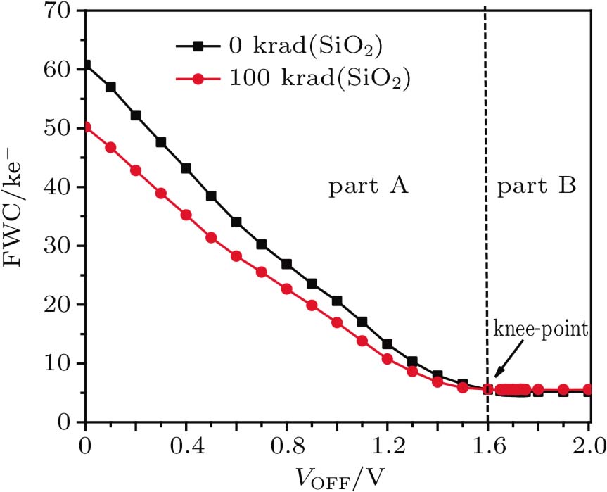
Fig. 7. (color online) Variations of FWC with VOFF for VOFF voltages ranging from 0 V to 2 V before and after irradiation.
Fig. 8. (color online) PD depletion region expanding after irradiation as illustrated by TCAD simulation.[14]
3.3. Ionizing effect leading to degradation of quantum efficiency

When the PPD is illuminated by a source of light on the top surface, the absorption of the incoming photons produces photo-electrons, for energy higher than the band gap of silicon. Quantum efficiency (QE) is an important parameter of the image sensor, characterizing the ability to convert photons of a certain wavelength into an effective electrical signal.[15]

The curve below displays the variations of QE with wavelength for visible spectrum (400 nm–1000 nm), as shown in Fig. 9, before and after γ irradiation. This measurement was performed on the monochromatic sensor without using a micro-lens. One can see that the QE has a clear drop after irradiation at shorter wavelengths, while there is no evidence of changes at longer wavelengths.

Fig. 9. (color online) Variations of QE with wavelength before and after irradiation.

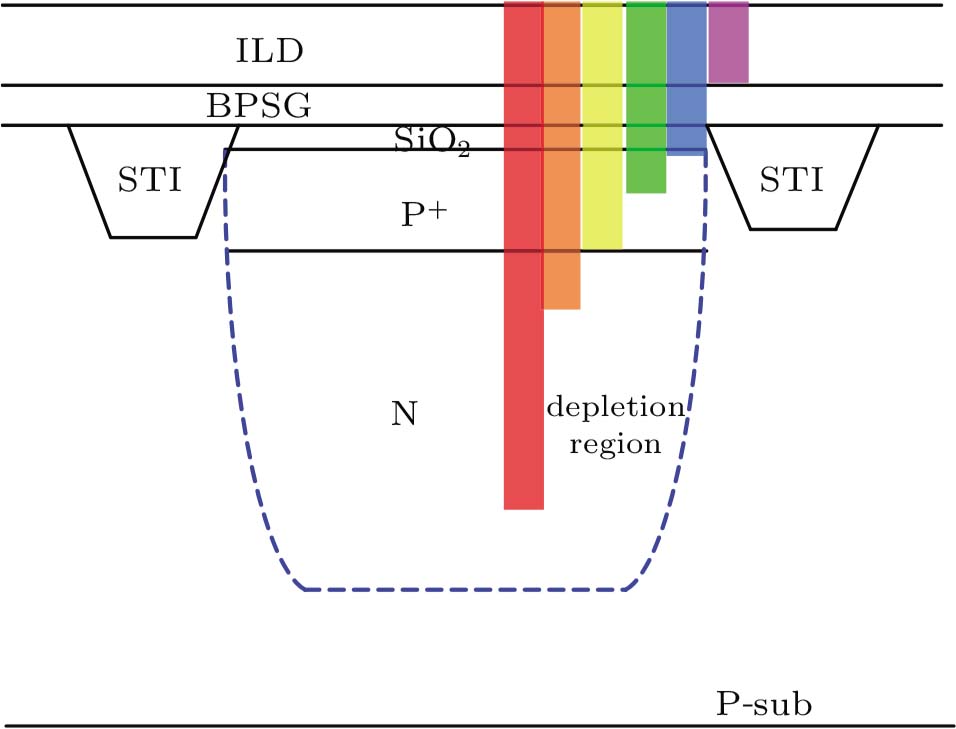
As shown in Fig. 10, the absorption depth decreases with wavelength decreasing. So, the electrons generated by shorter wavelengths are mainly located near the Si–SiO2 interface or STI and part of them diffuse into the depletion region. The diffusion length near the interface depends on the recombination lifetime, which corresponds to the Shockley–Read–Hall (SRH) mechanism, owing to the energy levels created by defects.[16] Hence, the decrease of collection efficiency at shorter wavelengths can be explained by the increase of the interface state density. All this tends to reduce the carrier recombination lifetime near the interface.

Fig. 10. (color online) Sketch of absorption depth at different wavelengths.
3.4. Analysis of annealing result

Figure 11 illustrates that the dark currents decrease with annealing time increasing at 100 °C and 200 °C. The dark current recovers about 30% of its post-irradiation value after being annealed at 100 °C for 168 h, and almost disappears during being annealed at 200 °C for 168 h. Most of the interface states encountered in the last decade of CMOS technologies are known to be annealed at high temperature (above 150) while trapped oxide charges are known to disappear after being annealed at 100 °C.[17] This corresponds to a dark current degradation mechanism where both interface states and trapped oxide charges are responsible for the growing of sensor dark current. It can be found that the annealing of traps induced by irradiation mostly take place at the beginning stage.

Fig. 11. Variations of dark current with annealing time at different temperatures.
4. Conclusions and perspectives

The radiation effects on PPD CMOS active pixel sensor caused by γ-ray are investigated. We study the degradation in the dark current, full well capacity, and quantum efficiency due to total ionizing damage effects.

After being exposed to irradiations up to 100 krad (SiO2), the device has a performance penalty. We find a considerable increase in the dark current, which is generated mainly by traps located at the STI interface and induced by damage at the same time, and the dark current from TG at a nominal VOFF of 0 V is negligible. The pinning voltage of the photodiode shows no changes with TID; on the contrary, the full well capacity is observed to decrease due to photodiode capacitance decreasing. The decrease of quantum efficiency at shorter wavelengths can be explained as that the increase of surface interface trap density results in the increase of photo-generated carriers recombination rate and the decrease of effective diffusion length.

Finally, most of the previous experiments have been performed on devices grounded during irradiation, which may hide some effects that could be enhanced by the local electric field during exposure to the irradiation. In order to investigate the potential biasing effects, more PPD CMOS sensors need to be irradiated by γ-ray under different biasing conditions.

Reference
[1] Wang F Li Y D Guo Q Wang B Zhang X Y Wen L He C F 2016 Acta Phys. Sin. 65 024212 in Chinese
[2] Wu K T Hwang S J Lee H H 2017 Sensors 17 1004
[3] Xue Y Wang Z Chen W Liu M He B Yao Z 2017 Sensors 17 2781
[4] Hopkinson G R 2000 IEEE Trans. Nucl. Sci. 47 2480
[5] Cohen M David J P 2000 IEEE Trans. Nucl. Sci. 47 2485
[6] Eid E S Chan T Y Fossurn E R Tsai R H 2001 IEEE Trans. Nucl. Sci. 48 1796
[7] Goiffon V Magnan P SaintPe O Bernard F Roll G 2008 IEEE Trans. Nucl. Sci. 55 3494
[8] Coath R E Crooks J P Godbeer A Wilson M D 2009 IEEE Nucl. Sci. Symposium Conference Record 57 1310
[9] Rao P R Wang X Theuwissen A J 2008 Solid-State Electron. 52 1407
[10] Goiffon V Virmontois C Magnan P Cervantes P Place S Gaillardin M Martin G P 2012 IEEE Trans. Nucl. Sci. 59 918
[11] Mheen B Song Y J Theuwissen A J P 2008 IEEE Electron Dev. Lett. 29 347
[12] Pelamatti A Goiffon V Estribeau M Cervantes P Magnan P 2013 IEEE Electron Dev. Lett. 34 900
[13] Krymski A Konstantin F 2005 Proc. IEEE Workshop CCD Adv. Image Sensors
[14] Vincent G Magali E Olivier M 2012 IEEE Trans. Nucl. Sci. 59 2878
[15] Cao C Zhang B Wu L S Li N Wang J F 2014 Chin. Phys. 23 124215
[16] Puliyankot V Raymond J H 2012 IEEE Electron Dev. 59 26
[17] Oldham T R Mclean F B 2003 IEEE Trans. Nucl. Sci. 50 483