Project supported by the National Natural Science Foundation of China (Grant Nos. 50972129 and 50602039), the International Science Technology Cooperation Program of China (Grant No. 2014DFR51160), the National Key Research and Development Program of China (Grant No. 2016YFE0133200), European Unio’s Horizon 2020 Research and Innovation Staff Exchange (RISE) Scheme (Grant No. 734578), One Belt and One Road International Cooperation Project from the Key Research and Development Program of Zhejiang Province, China (Grant No. 2018C04021), and Xinmiao Talents Program of Zhejiang Province, China (Grant No. 2017R403078).
Project supported by the National Natural Science Foundation of China (Grant Nos. 50972129 and 50602039), the International Science Technology Cooperation Program of China (Grant No. 2014DFR51160), the National Key Research and Development Program of China (Grant No. 2016YFE0133200), European Unio’s Horizon 2020 Research and Innovation Staff Exchange (RISE) Scheme (Grant No. 734578), One Belt and One Road International Cooperation Project from the Key Research and Development Program of Zhejiang Province, China (Grant No. 2018C04021), and Xinmiao Talents Program of Zhejiang Province, China (Grant No. 2017R403078).
† Corresponding author. E-mail:
Project supported by the National Natural Science Foundation of China (Grant Nos. 50972129 and 50602039), the International Science Technology Cooperation Program of China (Grant No. 2014DFR51160), the National Key Research and Development Program of China (Grant No. 2016YFE0133200), European Unio’s Horizon 2020 Research and Innovation Staff Exchange (RISE) Scheme (Grant No. 734578), One Belt and One Road International Cooperation Project from the Key Research and Development Program of Zhejiang Province, China (Grant No. 2018C04021), and Xinmiao Talents Program of Zhejiang Province, China (Grant No. 2017R403078).
We investigate the structural and electrical properties of carbon-ion-implanted ultrananocrystalline diamond (UNCD) films. Impedance spectroscopy measurements show that the impedance of diamond grains is relatively stable, while that of grain boundaries (GBs) (Rb) significantly increases after the C+ implantation, and decreases with the increase in the annealing temperature (Ta) from 650 °C to 1000 °C. This implies that the C+ implantation has a more significant impact on the conductivity of GBs. Conductive atomic force microscopy demonstrates that the number of conductive sites increases in GB regions at Ta above 900 °C, owing to the formation of a nanographitic phase confirmed by high-resolution transmission electronic microscopy. Visible-light Raman spectra show that resistive trans-polyacetylene oligomers desorb from GBs at Ta above 900 °C, which leads to lower Rb of samples annealed at 900 and 1000 °C. With the increase in Ta to 1000 °C, diamond grains become smaller with longer GBs modified by a more ordered nanographitic phase, supplying more conductive sites and leading to a lower Rb.
Diamond films have excellent properties such as high hardness, good chemical stability, and high thermal conductivity.[1–3] Ultrananocrystalline diamond (UNCD) film is a unique form of carbon, in which diamond grains with sizes of 3–5 nm are surrounded by an amorphous carbon matrix. UNCD films have applications where high conductivities are required, including electrochemical electrodes,[4–6] field emission,[7] and heterostructures.[8,9] Extensive studies have been performed to improve the conductivities of UNCD films. It has been reported that nitrogen-doped UNCD films exhibit n-type conduction with an enhanced electrical conductivity, which is attributed to the increased number of sp2 bonds at grain boundaries (GBs).[10,11] Phosphorous and oxygen ion implantations were used to increase the conductivity of nanocrystalline diamond grains and amorphous-carbon GBs, which improved the n-type Hall mobility of the UNCD film.[12,13] A hybrid structure of UNCD and graphene nanoribbons promoted a high mobility and n-type conductivity in an oxygen-ion-implanted UNCD film.[14] Lithium ion implantation induced the formation of electron trap centers inside diamond grains, whereas post-annealing healed the defects and converted the amorphous carbon phase into nanographite, forming conduction channels for an effective transport of electrons.[7]
Amorphous carbon in GBs is a common component in UNCD films, whose electrical conductivities were reported to be not sufficiently high, thus limiting the applications of UNCD films.[15] It is believed that the conversion of amorphous carbon to a conducting graphitic phase along GBs enhances the efficiency for electron transport on the surface, thus improving the conductivity of the UNCD film.[16,17] It was also reported that copper[18] and gold[19] ion implantations and annealing promoted electrical properties of UNCD films by decreasing the amorphous carbon content and even by inducing the nanographitic phase in GBs. This suggests that the electrical properties can be effectively improved by modifying the structure and component of amorphous-carbon GBs. Carbon ions are not dopants for diamond grains, but preferentially lead to more ordered amorphous-carbon GBs to enhance the conduction mobility. A high-dose C+-ion implantation (1015 cm−2) and annealing lead to crystallization of the graphite phase that was not transformed from amorphous carbon in the UNCD film and degradation of the field-emission properties.[20] In this study, we implanted a lower dose of C+ to regulate the microstructures of the UNCD films particularly in GBs to improve their electrical properties. High-resolution transmission electronic microscopy (HRTEM) and visible-light Raman spectroscopy were used to characterize the microstructures of the films after ion implantation and annealing. Conductive atomic force microscopy (AFM) was used to acquire images of conductive capacities at different parts of the UNCD films. Impedance spectroscopy (IS) was employed to distinguish the conductivity contributions from diamond grains and GBs.
The results show that the impedance resistance of GBs significantly increases after the C+ implantation; it is effectively reduced with the increase in the annealing temperature (Ta) in the range of 650–1000 °C. The impedance of diamond grains is relatively stable. This suggests that the C+ implantation has a larger impact on the impedance of GBs than on diamond grains. When Ta is above 900 °C, the number of conductive sites significantly increases in the GB region of the UNCD film owing to the formation of a nanographitic phase, which is responsible for the reduced impedance resistance of the GBs.
UNCD films were deposited using a hot-filament chemical vapor deposition (HFCVD) system on single-crystal silicon (111) wafers. The carbon source was acetone, the volume ratio between acetone and hydrogen was 1%–2% with a total gas flow of 200 ml/min, the working pressure in the reaction chamber was 0.5–1.4 kPa, and the temperature of the substrate was approximately 850 °C. The thickness of the as-deposited UNCD films was approximately 5 μm, obtained at a growth rate of 1.5 μm/h. C+ implantation was performed on as-deposited UNCD films with an implantation energy of 90 keV and dose of 1012 cm−2. For room-temperature implantations, there is a universal critical damage density (1022 vacancies/cm3), which, when exceeded, leads to complete graphitization of heavily damaged diamond crystals upon annealing.[21] It was shown that the C+ implantation level of 1012 cm−2 at room temperature was significantly below the critical dose of (2 − 3) × 1015 cm−2.[22] The implantation profile was determined by the Stopping and Range of Ions in Matter (SRIM-2013) software. C ions were implanted into diamond with an average ion range of 121 nm, creating 1019 vacancies/cm3 in the meantime. The implanted samples were annealed at 500, 650, 725, 800, 900, and 1000 °C for 30 min at a pressure of 4000 Pa (80% N2 and 20% O2), denoted as C12500, C12650, C12725, C12800, C12900, and C121000, respectively. The annealing at 900 °C for 30 min was performed on an as-deposited UNCD film (sample 900-A) to distinguish the effects of C+ implantation and annealing on the electrical properties of the UNCD films.
HRTEM was used to characterize the microstructures of the films using a Tecnai G2 F30 S-Twin microscope, produced by Philips-FEI. Visible-light Raman spectroscopy measurements (JobinYvon, Labor Raman HR-800) of the samples were performed with an excitation wavelength of 514 nm at room temperature. Conductive AFM and scanning Kelvin microscopy (SKM) were performed in a scanning probe microscope (SPM) (Solver P47, NT-MDT, Russia) under ambient conditions.
Ti (500 nm)/Au (300 nm) contacts were fabricated using an SPC-350 magnetron sputtering system with a metal mask covering on the UNCD films set before the deposition. The metal mask was fixed by a high-temperature tape with the UNCD film to ensure its stability during the deposition. The contacts were then annealed under a vacuum at 450 °C for 20 min. The diameter of the electrode was 2 mm. I–V measurements of the samples at room temperature showed that ohmic contacts were formed. The impedance properties of the samples were determined using an Autolab potentiostat–galvanostat connected with a four-probe station in the frequency range of 0.01 Hz to 10 MHz. IS was employed to study the electrical properties of single-crystal diamond and polycrystalline diamond. This technique involves a measurement of the real and imaginary components of the film impedance as a function of both frequency and temperature. The impedance as a complex number can be defined as
 |
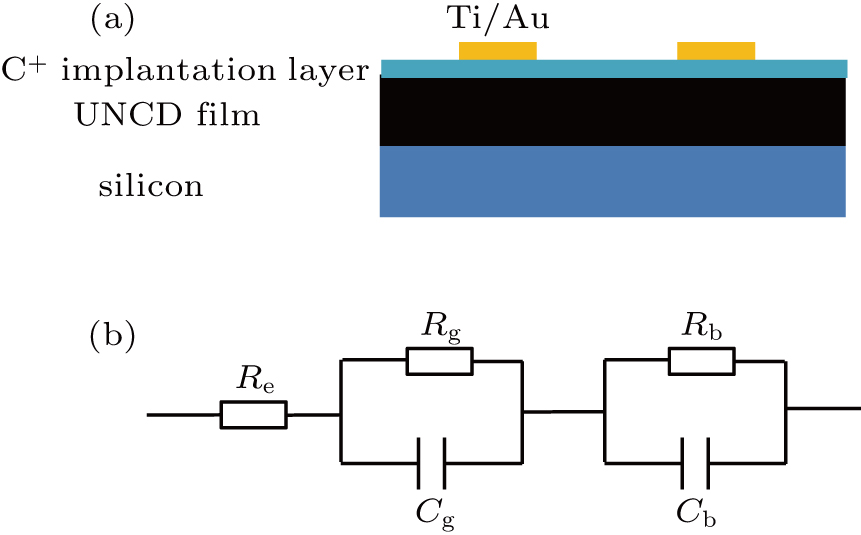
Theoretically, a double RC parallel model in series could be used to simulate the electrical conduction of diamond films attributed to uniformly distributed diamond grains and GBs, as illustrated in Fig.
The complex impedance can be expressed as
 |
 |
I–V measurements were performed before the IS measurements to ensure that ohmic contacts were formed between the electrodes and UNCD films. Figure
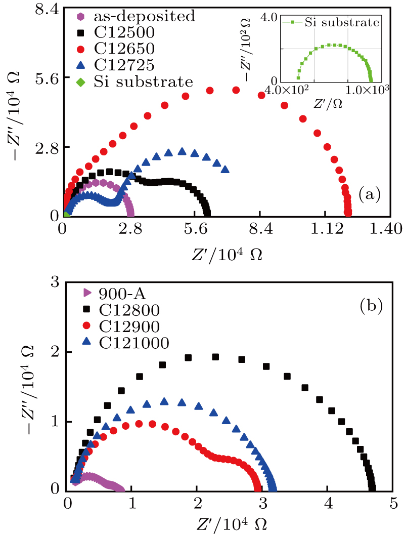
Figure
The resistance and capacitance values were obtained according to the equivalent circuit model and presented in Table
The Re values presented in Table
| Table 1.
Resistance and capacitance values of the as-deposited sample, sample 900-A, and C+-implanted samples. . |
The Rb value of sample 900-A is 2.2 kΩ, slightly higher than that of the as-deposited sample of 1.4 kΩ. The Rb value of sample C12500 is 26 kΩ; it significantly increases to 97.4 kΩ for sample C12650. It starts to decrease when Ta further increases, reaching a value of 6.6 kΩ for sample C121000. These Rb values are higher than that of the as-deposited sample, which implies that the C+ implantation increases the impedance of GBs even though it is effectively reduced by the annealing.
The IS results show that the contribution of diamond grains to the conductivity is increased after the C+ implantation and annealing. The significantly increased Rb values of the C+-implanted samples decrease with the increase in Ta in the range of 650–1000 °C, while the Rg values remain stable, which indicates that the C+ implantation has a larger impact on the impedance of GBs. The lower Rb values of samples C12900 and C121000 show that their GB regions are more conductive than those of the C+-implanted samples annealed at lower Ta.
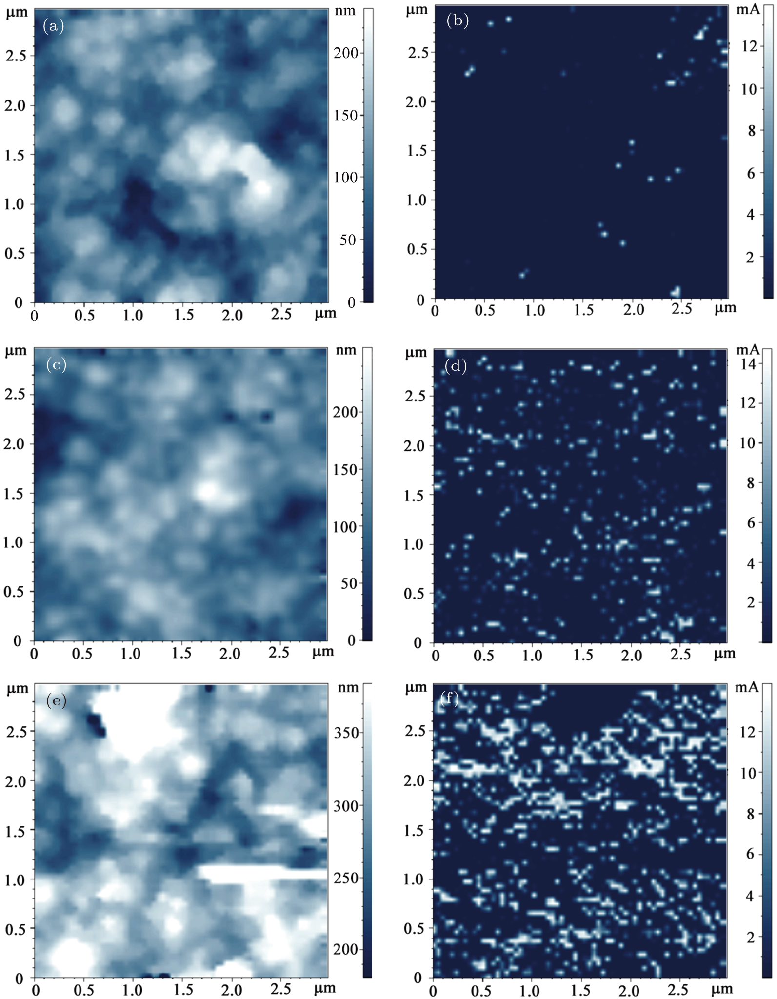
In order to observe the conductive behavior at the microscale, conductive-AFM and SKM were employed. A Pt-coated Si cantilever with a tip curvature radius of ∼ 35 nm was used to obtain the surface height relief in the tapping mode. Local conductance was scanned in the contact mode across a previously detected surface-height-relief map (with a sample–probe gap of Δ = 0). At each point, a bias voltage is applied between the sample and grounded probe to obtain the surface conductivity. Therefore, the local conductance represents the conductive behavior of the ion-implanted layer. A sample–probe gap of Δ = 100 nm was used during the SKM measurements. For each sample, the measurements were repeated at 5 arbitrarily chosen 3 × 3 μm2 regions. Figure
 | Fig. 3. (color online) Surface height-relief maps of samples (a) C12725, (c) C12900, and (e) C121000, and local conductances of samples (b) C12725, (d) C12900, and (f) C121000 at U = 2 V. |
Figure
 | Fig. 4. (color online) (a) Conductance and (b) contact-potential histograms of samples C12725, C12900, and C121000 obtained from conductive-AFM measurements. |
The increased numbers of conductive sites in samples C12900 and C121000 indicate that the microstructure changes in the GB regions. In order to understand the origin of these highly conductive GBs, we performed HRTEM measurements to characterize the microstructures of the as-deposited sample and samples C12900 and C121000. During the TEM specimen preparation, first, the Si substrate was removed and then the UNCD film close to the Si side was removed by argon-ion milling, providing surface area (ion implantation region) for observation. Figures
Figure
Figure
Figure
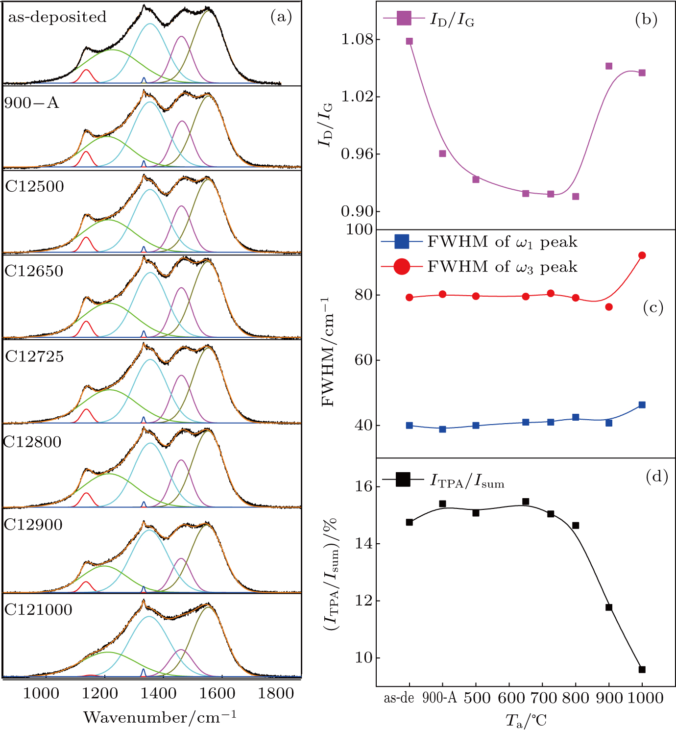
In order to further investigate the microstructure changes of GBs in the C+-implanted samples, visible-light Raman spectra in the range of 800–2000 cm−1 for the as-deposited sample, sample 900-A, and C+-implanted films are shown in Fig.
Figure
IS results show that the Rg is relatively stable, while the Rb significantly increases after the C+ implantation, which indicates that the contribution of diamond grains is increased after the ion implantation. The Rb gradually decreases with the increase in Ta in the range of 650–1000 °C, which implies that the C+ implantation has a larger impact on GBs than on diamond grains. The IS and AFM results demonstrate that the number of conductive sites in the GBs increases with Ta in the range from 725 °C to 1000 °C. The HRTEM and AFM results demonstrate that the number of conductive sites in GBs increases at Ta higher than 900 °C owing to the formation of the nanographitic phase. Visible-light Raman spectra and HRTEM results show that the nanographitic phase is more ordered in sample C121000 than that in sample C12900, which provides more conductive sites and leads to the lower Rb of sample C121000.
We showed that the C+ implantation significantly increased the impedance resistance of GBs, which was effectively reduced with the increase in Ta in the range of 650–1000 °C, while the impedance resistance of diamond grains was relatively stable in UNCD films. This suggested that the C+ implantation had a larger impact on the impedance of GBs than on that of diamond grains. Conductive-AFM results demonstrated that the number of conductive sites in GBs significantly increased when Ta was above 900 °C owing to the formation of a nanographitic phase, confirmed by HRTEM. Visible-light Raman spectra and HRTEM results showed that the nanographitic phase was more ordered in sample C121000 than in sample C12900, which further decreased the Rb of sample C121000.
| [1] | |
| [2] | |
| [3] | |
| [4] | |
| [5] | |
| [6] | |
| [7] | |
| [8] | |
| [9] | |
| [10] | |
| [11] | |
| [12] | |
| [13] | |
| [14] | |
| [15] | |
| [16] | |
| [17] | |
| [18] | |
| [19] | |
| [20] | |
| [21] | |
| [22] | |
| [23] | |
| [24] | |
| [25] | |
| [26] | |
| [27] | |
| [28] | |
| [29] | |
| [30] | |
| [31] | |
| [32] | |
| [33] | |
| [34] | |
| [35] | |
| [36] | |
| [37] |


