Yang Longkun, Li Pan, Wang Hancong, Li Zhipeng. Surface plasmon polariton waveguides with subwavelength confinement*
Project supported by the National Natural Science Foundation of China (Grant Nos. 11704266 and 11774245), the Fok Ying Tung Education Foundation, China (Grant No. 151010), the Scientific Research Base Development Program of Beijing Municipal Commission of Education, China, the General Foundation of Beijing Municipal Commission of Education, China (Grant No. KM201810028006), and the Training Program of the Major Research Plan of Capital Normal University, China.
. Chinese Physics B, 2018, 27(9): 094216
Permissions
Surface plasmon polariton waveguides with subwavelength confinement*
Project supported by the National Natural Science Foundation of China (Grant Nos. 11704266 and 11774245), the Fok Ying Tung Education Foundation, China (Grant No. 151010), the Scientific Research Base Development Program of Beijing Municipal Commission of Education, China, the General Foundation of Beijing Municipal Commission of Education, China (Grant No. KM201810028006), and the Training Program of the Major Research Plan of Capital Normal University, China.
Yang Longkun1, Li Pan1, Wang Hancong2, Li Zhipeng1, †
The Beijing Key Laboratory for Nano-Photonics and Nano-Structure (NPNS), Center for Condensed Matter Physics, Department of Physics, Capital Normal University, Beijing 100048, China
The Fujian Provincial Key Laboratory of Automotive Electronics and Electric Drive, School of Information Science and Engineering, Fujian University of Technology, Fuzhou 350108, China
† Corresponding author. E-mail: zpli@cnu.edu.cn
Project supported by the National Natural Science Foundation of China (Grant Nos. 11704266 and 11774245), the Fok Ying Tung Education Foundation, China (Grant No. 151010), the Scientific Research Base Development Program of Beijing Municipal Commission of Education, China, the General Foundation of Beijing Municipal Commission of Education, China (Grant No. KM201810028006), and the Training Program of the Major Research Plan of Capital Normal University, China.
Abstract
Surface plasmon polaritons (SPPs) are evanescent waves propagating along metal–dielectric interfaces, which provide an effective way to realize optical wave guiding with subwavelength confinement. Metallic nanostructures supporting SPPs, that is, plasmonic waveguides, are considered as required components to construct nanophotonic devices and circuits with a high degree of miniaturization and integration. In this paper, various types of plasmonic waveguides operating in the visible, infrared, and terahertz regions are reviewed, and the status of the research on their fundamentals, fabrications, and applications is provided as well. First, we discuss the mechanisms of SPPs beyond the diffraction limit, and their launching methods. Then, the characteristics of SPPs on various plasmonic waveguides are reviewed, including top-down and bottom-up fabricated types. Considering applications, certain prototypes of plasmonic devices and circuits constructed by plasmonic waveguides for bio/chemo sensing, router, and light modulation are demonstrated. Finally, a summary and future outlook of plasmonic waveguides are given.
An optical waveguide is a kind of dielectric microstructure which can confine the propagation of optical waves in one or two dimensions with minimal energy loss. Owing to their unique advantages in information transmission, such as high speed, large capacity, and anti-interference, optical waveguides have been crucial components in photonic circuits performing optical signal guiding,[1] coupling,[2] switching,[3] splitting,[4] multiplexing,[5] and so on. To fulfill the increasing demand for information processing and computing, several efforts have been devoted to the miniaturization and high-density integration of photonic circuits. However, the diffraction limit of light restricts the size of dielectric optical waveguides, that is, half of the effective wavelength.[6] Fortunately, surface plasmons, which are collective electron oscillations of noble metal nanostructures, provide an effective approach to address the problems of the diffraction limit.[7–10] When light couples with metal nanostructures, the excitation of surface plasmons can transform the free-space light into plasmon modes, which are highly confined at the metal surface, enabling light manipulation at nanometer scale. Depending on the dimensions of the confinement, excited surface plasmons can be categorized as localized surface plasmons resonances (LSPRs) and propagating surface plasmon polaritons (SPPs). LSPRs are typically excited in nanostructures which are significantly smaller than the incident wavelength, such as nanoparticles and their coupling geometries,[11–15] and have important applications in ultrasensitive detection and sensing.[16–19] SPPs are propagating electromagnetic waves with their field tightly confined at the interfaces between metals and dielectrics,[20–23] similarly to light guided by optical fibers. In this review, for the purpose of information transmission and ultra-compact photonic circuits integration, only the propagating SPPs with subwavelength confinement are considered. So far, various metallic nanostructures have been fabricated to support SPPs, known as plasmonic waveguides, such as thin metal films, insulator/metal/insulator slabs, metal/insulator/metal slabs, metal stripes, metal grooves, or chemically synthesized metal nanowires (NWs). These plasmonic waveguides have been considered to be among the best components to construct the nanophotonic devices to realize light manipulation at nanometer scale, and certain simple plasmonic circuits have recently been accomplished.[24–30]
In this review, our aim is to present various plasmonic waveguides operating at visible, infrared and terahertz regions and to provide the status of the research on their fundamentals, fabrications, and applications. We begin with a discussion of the fundamentals of SPPs beyond the diffraction limit in Section 2, while the methods used to launch the SPPs are also presented. In Section 3, the surface plasmon propagation in various plasmonic waveguides are reviewed. Here, we divide the plasmonic waveguides into top-down fabricated, such as the metal stripes, grooves, and periodically corrugated metal strips, and bottom-up fabricated, such as chemically synthesized gold and silver nanowires. In Section 4, some simple plasmonic components and circuits constructed by plasmonic waveguides are reviewed. Finally, a summary and a future outlook on plasmonic waveguides are given.
2. SPP waveguides with subwavelength confinement
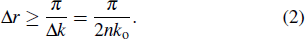
In dielectric waveguides, optical waves are confined and guided by the total internal reflection at the dielectric interface. The dispersion relation of light propagating in dielectric waveguide with an angular frequency ω can be expressed as
where k = nko = 2πn/λo is a wavevector in the dielectric, n is the refractive index of the dielectric, and εd is the relative permittivity of the dielectric. The dispersion curve is shown in Fig. 1(a). As all components of the optical wave are real, kj (j = x, y, z) has the value satisfying −nko ≤ kj ≤ nko, which means that the range of the wavevector in the dielectric is Δk = 2nko. According to the uncertainty relation of Fourier transforms, Δk and the range of real space Δr satisfy Δr · Δk ≥ π. Therefore, Δr has a minimum given by the following relation:
Considering that the refractive indexes of dielectrics are real constants, equation (2) determines the minimum size of an optical beam, which is limited to the order of ( nko)−1, that is, the diffraction limit.[6] As a result, when the diameter D of the fiber is decreased to the subwavelength, the guided mode deeply penetrates into the surrounding medium, and eventually (at D = 0) becomes a bulk plane-wave in the medium surrounding the waveguide (Fig. 1(b)).[8] Thus, decreasing the diameter of an optical fiber or other dielectric waveguides does not result in the subwavelength localization of the guided mode. To achieve a higher degree of miniaturization of waveguides and integration to optical devices, the problem of diffraction limit of optical waveguides needs to be addressed.
Fig. 1. (color online) (a) Dispersion relations for spatial light and SPPs. (b) Typical field structures and localization of the fundamental modes guided by dielectric (upper) and metal (lower) waveguides, where λ represents the mode wavelengths. The dashed horizontal lines show the localization of the mode at the 1/e level of the field.
Nevertheless, by comparing with the spatial light in the dielectric waveguide, the dispersion relationship of SPPs propagating along the dielectric-metal interface is significantly different. As shown in Fig. 1(a), the wavevector of SPPs, kspp, can be expressed as[31]
where n is the refractive index of the dielectric, εd and εm are the relative permittivity of the dielectric and the metal, respectively, and ωp is the frequency of the plasmons. According to the Lorentz–Drude model, the relative permittivity of the metal is a complex number with a negative real part for the visible and the infrared regions. As a result, if the real part of the relative permittivity satisfies Re(εm) < −εd, according to Eq. (3), the real part of the wavevector of the SPP can be expressed as
indicating that the range of the SPP wavevector satisfies Δ Re(kspp) > 2nko; thus, a much lower Δr can be acquired. This implies that the SPP waveguides can resolve the restriction of the diffraction limit and enable the guiding of light with subwavelength confinement (Fig. 1(b)).
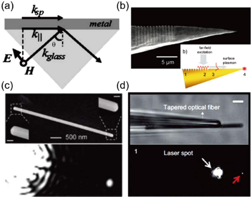
As photonic components, the SPP-based plasmonic waveguides are expected to be able to interface with the real optical environment; however, the wavevector of SPPs is larger than that of free space light. Therefore, special experimental arrangements need to be designed to ensure the necessary wavevector conservation during the conversion of photons to surface plasmons. A typical method to launch SPPs at the metal–dielectric interface is to employ the attenuated total reflection in the Kretschmann configuration (prism coupling),[32] which allows the matching of the SPPs wavevector with the parallel component of light wavevector (Fig. 2(a)). Another method to ensure wavevector conservation for SPP excitation is to use diffraction effects. By fabricating a diffraction grating on a section of a smooth metal film, components of the diffracted light whose wavevectors coincide with the SPPs can launch surface plasmons (Fig. 2(b)).[33] Individual nanoscale structures, such as defects, nanoantennas, and nanowire termination, can also be used for light–SPPs coupling, as light scattered at such structures have a wide range of wavevectors,[34–37] and part of the scattered light can match with the wavevectors of SPPs. For example, SPPs on a silver nanowire can be launched directly by focusing the light on one of the terminations (Fig. 2(c)).[38] Although far-field illumination cannot launch SPPs directly, the application of a near-field microscope provides a novel approach to excite SPPs locally. Two kinds of excitation mechanisms are proposed: diffraction and tunneling. For instance, SPPs on silver nanowires can be launched by optical fiber in an “end-fire” configuration (Fig. 2(d)).[39,40]
Fig. 2. (color online) SPP excitation configurations. (a) Kretschmann configuration for prism coupling, reproduced from Ref. [32]. (b) Diffraction on a grating structure, reproduced from Ref. [33]. (c) Scattering on nanowire termination, reproduced from Ref. [38]. (d) Excitation by near-field end-fire configuration, reproduced from Ref. [39].
Except for light excitation, SPPs can be directly launched by electrons.[41] For a focused electron beam, the electric field around the moving electrons contains Fourier components of all frequencies; therefore, plasmons at different frequencies can be excited simultaneously due to the Coulomb interaction, as shown in Fig. 3. Combining electron energy loss spectroscopy (EELS) with a transmission electron microscope (TEM), the plasmon behaviors on various metal nanostructures can be studied in situ.
Fig. 3. (color online) Excitation of SPPs on an Au nanowire by electrons (100 keV). Left panel: Probability of energy-loss of electrons passing at a distance of 10 nm from the surface of a free-standing Au nanowire. Right panel: EELS probability integrated over parallel momentum (solid curve) and partial contributions of SPP modes (dash lines), reproduced from Ref. [41].
3. SPP propagation on different waveguides
SPP-based waveguides allow light to be concentrated into regions as small as a few nanometers, limited only by the atomic structure of matter, propagation loss, and the dispersion relation. Based on the fabrication methods, plasmonic waveguides can be categorized into top-down fabricated and bottom-up fabricated types.
3.1. Top-down fabricated plasmonic waveguides
The top-down approach refers to the nanofabrication method starting from bulk materials and subsequently using finer tools to create the designed nanostructures. Currently, the most commonly used nanofabrication techniques for metal nanostructures are electron beam lithography and focused ion beam milling.[42–44] By exploiting the development of nanofabrication techniques, the precise control over metal patterns at nanometer scale has been accomplished, which significantly accelerates the fundamental studies and practical applications of metal plasmonics.[45–47] In this section, we focus on the review of top-down fabricated plasmonic waveguides, such as metal stripes, grooves, and ultrathin corrugated metal strips.
3.1.1. Metal stripes
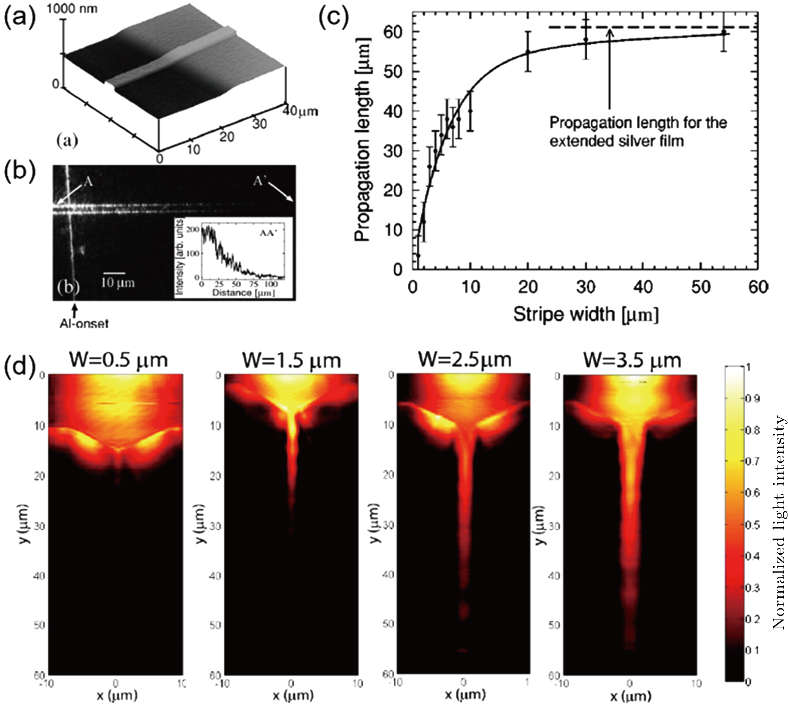
A metal stripe refers to a symmetric thin metal film (with a typical thickness below 100 nm) with its width customized from the micron to the nanometer scale. Pierre Berini discussed the dispersion characteristics of SPP modes on metal stripes first, which provided the fundamentals to use them as plasmonic waveguides.[48] Generally, SPPs on these metal stripes can be launched by a prism-coupling arrangement, as described in Section 2. By measuring the light scattered from the surface roughness, the width-dependent 1/e SPP propagation length (LSPP) on silver stripes (with a thickness of 70 nm) was investigated (Figs. 4(a) and 4(b)).[49] As shown in Fig. 4(c), for widths larger than 20 μm, the LSPP is very close to the value of the extended film, while the LSPP drastically decreases to a few micrometers for a 1 μm stripe width. Krenn et al. also reported that even for a gold stripe with a cross-section (λ/4 × λ/16) far below the diffraction limit, an LSPP of 2.5 μm can still be achieved.[50] This width-dependent LSPP on metal stripes can also be directly visualized by near-field measurements using photon scanning tunneling microscope (PSTM).[51,52] As shown in Fig. 1(d), near-field images clearly demonstrate that the LSPP decreases with the decrease of the width of metal stripes.
Fig. 4. (color online) (a) The atomic force microscope (AFM) image of a 3-μm-wide and 70-nm-thick silver stripe. (b) Far-field scattered light image of an SPP propagating in the silver stripe. The inset shows the 1/e propagation length. (c) LSPP in 70-nm-thick silver stripes as a function of stripe width (λ = 633 nm), reproduced from Ref. [49]. (d) Near-field PSTM images of surface plasmons propagating along gold stripes with different widths (λ = 780 nm), reproduced from Ref. [51].
Besides the LSPP, another unusual feature of SPPs propagating along a metal stripe is their strong lateral confinement within the stripe width. In order to study this behavior, stripes of different widths attached to a gold thin film are fabricated by electron beam lithography (Fig. 5(a)).[53] Thin-film SPPs were launched by a Kretschmann configuration, which were then coupled into the stripes. To decrease the scattering loss and improve the excitation efficiency of the stripe SPPs, a tapered transition between the thin film and stripes is designed (Figs. 5(b) and 5(c)). The strong lateral confinement of the stripe SPPs can be visualized by comparing the PSTM image with the geometrical width of the stripe. As shown in Fig. 5(d), by superposing the transverse cross-cuts of the near-field optical images with the topographic stripe profiles (dashed lines), it can be clearly observed that the lateral confinements of the SPP modes become stronger with the decrease of the width, which is rather different from those of the standard dielectric waveguides. Hence, these metal stripe structures of finite widths can be plasmonic waveguides with an LSPP ranging from several to tens of micrometers and with a strong spatial confinement of SPP modes, which are promising for short-range optical communication applications in highly integrated nanophotonic devices.
Fig. 5. (color online) (a) SEM images of 55-nm-thick gold stripes. The widths of the stripes are in the range of 2–4.5 μm in steps of 0.5 μm. (b) AFM and (c) PSTM images of the tapered junction between the extended thin film and the 2.5-μ m-wide stripe shown in (a). (d) Transverse cross-cuts of the near-field intensity distribution recorded at a constant height over three of the stripes (widths of 4 μm, 2.5 μm, and 1.5 μm) shown in (a), reproduced from Ref. [53].
3.1.2. Metal triangular shaped grooves
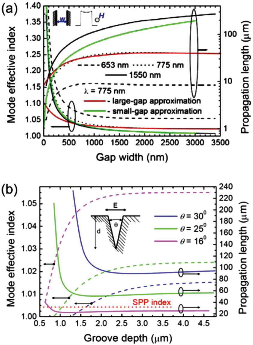
A metal triangular V-shaped groove is another typical structure, which can be employed as a plasmonic waveguide.[8,54,55] This V-groove configuration can be considered as a special type of gap waveguide (metal–insulator–metal (MIM)), whose width is monotonically decreases with the increase of the depth. For the MIM structure, with a narrow of gap width, the effective indexes of the SPPs modes increase, while the LSPP decreases correspondingly (Fig. 6(a)).[56,57] According to equation
of the mode penetration depth in dielectric, these results indicate that light is likely to be confined in the regions with high refractive indexes, although at the cost of increased losses. The V-groove shape can be represented as a stack of infinitesimally narrow MIM waveguides, each with an insulator width depending on the position, while the effective refractive index of each stack increases toward the bottom of the groove. Therefore, V-grooves with proper depth can support the bound modes formed by gap SPPs, which are confined to the bottom of the groove. These bound SPP modes propagating along the groove axis are known as channel plasmon polaritons (CPPs).[55] Figure 6(b) shows that with the reduction of the groove angle, θ, the CPP effective refractive index increases, while the LCPP decreases correspondingly.[56,57] Hence, the CPP modes are likely to be more confined at the bottom of groove when the angle decreases.[58] It can also be observed that the LCPP starts to increase rapidly when the groove depth decreases to a certain value, and a cut-off depth also exists, below which no CPP modes can be supported.
Fig. 6. (color online) (a) Effective indexes of the gap surface plasmon modes and their propagation length as a function of the width of the air gap between gold films. (b) Effective indexes of the fundamental CPP modes at 1.55 μm and their propagation lengths as a function of the groove depth for different θ groove angles, reproduced from Ref. [56].
Nevertheless, the dispersion characteristics of CPP modes (mode index, confinement, and propagation length) were also experimentally investigated by near-field optical microscopy.[59] As can be seen in Fig. 7(a), the V-grooves (θ ≃ 17°, d ≃ 1.7 μm) are fabricated by focused ion beam milling in a gold film. The CPPs in the groove can be launched by an end-fire coupling configuration (Fig. 7(b)). By scanning near-field optical microscope (SNOM) mapping, the CPPs propagating along the groove can be clearly visualized (Fig. 7(d)). It was found that the LCPP increases from ∼ 15 μm to 25 μm with the increase of the excitation wavelength from 1425 nm to 1600 nm. These experimental results of the wavelength-dependent LCPP are in good agreement with the simulations performed by effective index approximation and finite element method (FEM), as shown in Fig. 7(e). The CPP modes width (confinement) was also evaluated by measuring the full width at half maximum (FWHM) of the near-field optical signal, which was ∼ 200 nm and far below the diffraction limit. The distribution of the fundamental CPP mode was simulated by FEM method. With the increase of wavelength, the field of the CPP mode shifted progressively toward the groove opening (inset of Fig. 7(e)). A cutoff threshold (λcut > 1630 nm) can be identified, where the CPP mode was no longer confined at the groove bottom and became hybridized with plasmon modes running along the groove wedge. These results agree with the study by Moreno et al. using a multiple multipole method and a finite-difference time-domain technique.[60] Furthermore, based on Eq. (6), the effective indexes of the CPP modes were determined by exponentially fitting the dependence of the optical signal on the distance between the fiber tip and the groove bottom (Fig. 7(f)). In addition, for the design of nanocircuits, the bend loss in the plasmonic waveguides needs to be considered.[61,62] The loss of the CPP modes in the S-bends and Y-splitters (with the smallest curvature radius of ∼ 0.83 μm) were investigated using near-field optical microscopy (Fig. 7(g)). It was found that the losses in S-bends and Y-splitters decreased for longer wavelengths, and approached the levels of ∼ 0 dB and ∼ 0.5 dB, respectively, at 1640 nm. All these results demonstrate that the CPP modes guiding along the groove bottom are low-loss and well-confined at the subwavelength scale, which further strengthen the possibility of high-integrated photonic circuits. Certain simple plasmonic components based on the CPPs of V-grooves have been accomplished, such as the Mach–Zehnder interferometers,[63] waveguide-ring (WR) resonators,[63] add-drop multiplexers,[64] and compact Bragg grating filters.[64,65]
Fig. 7. (color online) (a) SEM image of the groove milled in a gold film. (b) CPPs launched by end-fire configuration. (c) Microscope image of the near-field optical probe. (d) SNOM images recorded at different wavelengths, in the range of 1425–1630 nm. (e) CPP dispersion: the CPP propagation length as a function of light wavelength. Insets show the electric field distributions of the fundamental CPP modes at different wavelengths. (f) Optical signal recorded inside the groove as a function of the distance between the probe and the bottom of the groove, together with the exponential fitting curves (dash lines), reproduced from Ref. [59]. (g) Near-field optical images taken at 1600 nm: (I) S-bends and (II) Y-splitter, reproduced from Ref. [62].
3.1.3. Periodically corrugated metal strips for spoof SPP waveguides
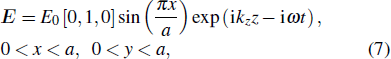
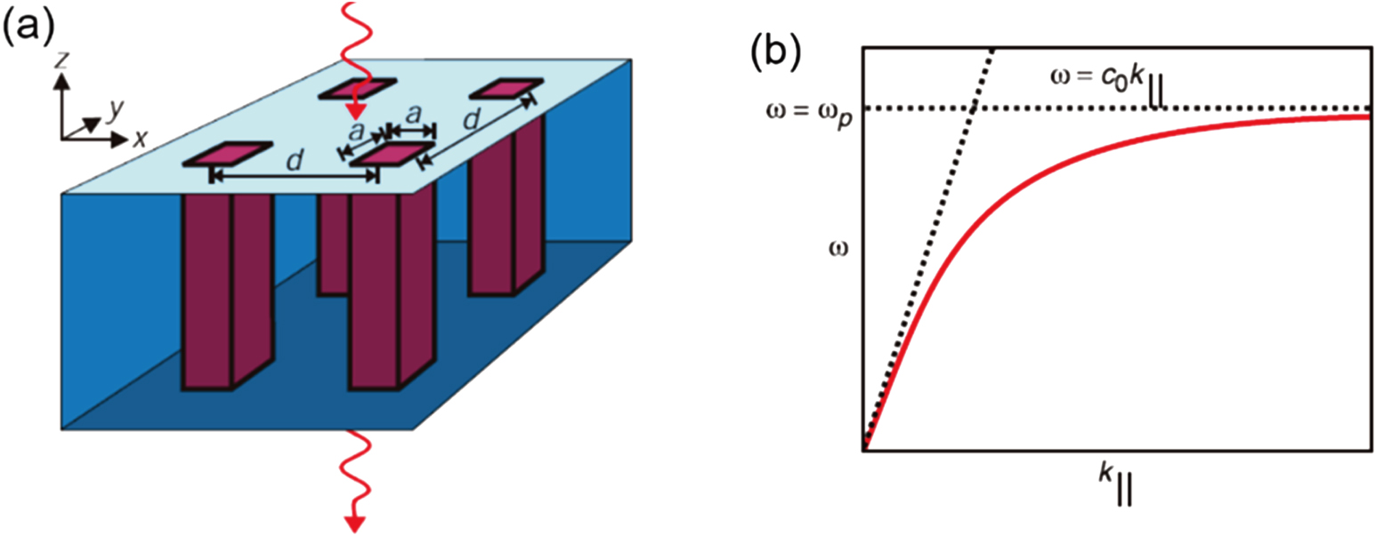
The metal strip and groove structures mentioned above are SPP waveguides operating at visible and near infrared regions, which demonstrate subwavelength confinement owing to the negative permittivity of metals below the plasmon frequency (Eq. (4)). However, as the frequency approaches the terahertz (THz) and microwave regions, metals behave as perfect electric conductors (PECs), owing to the infinite dielectric constant, rather than plasmons with negative permittivity. Hence, wave penetration into the metal becomes negligible and natural SPPs cannot be supported. To realize subwavelength-confined SPPs at low frequency, a structured surface decorating with periodic arrays of subwavelength holes was proposed by Pendry et al., which can support the surface waves mimicking real SPPs.[66] The model of the structured surface with subwavelength holes cut into a PEC is shown in Fig. 8(a). Following excitation, both the electric and magnetic fields are zero inside the PEC; however, in the holes, the electric field can be expressed as (considering the fundamental mode only)
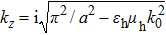
where E0 is a constant, k0 is the free space wavevector, , and εh and μh are permittivity and permeability, respectively, of materials filling the holes. According to Maxwell’s equations, the permittivity is given by
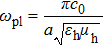
which is very similar to εm at visible and infrared regions (Eq. (4)). Here, by defining the plasmons frequency as , the dispersion relation of the surface plasmons, which can be supported by this structured surface can be expressed as
Figure 8(b) shows the dispersion relation curve of this surface wave in the hole, which is very similar to those of natural SPPs in metal structures; thus, these are also known as spoof surface plasmons. These spoof SPPs were further verified experimentally by Hibbins et al.,[67] which opened the way to plasmonic studies at the terahertz and microwave regimes.
Fig. 8. (color online) (a) Model of the structured surface with square holes cut into the PEC. (b) Dispersion relation for spoof surface plasmons on the structured surface, with the asymptotes of the light line at low frequencies and the plasmon frequency at large values of k||, reproduced from Ref. [66].
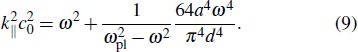
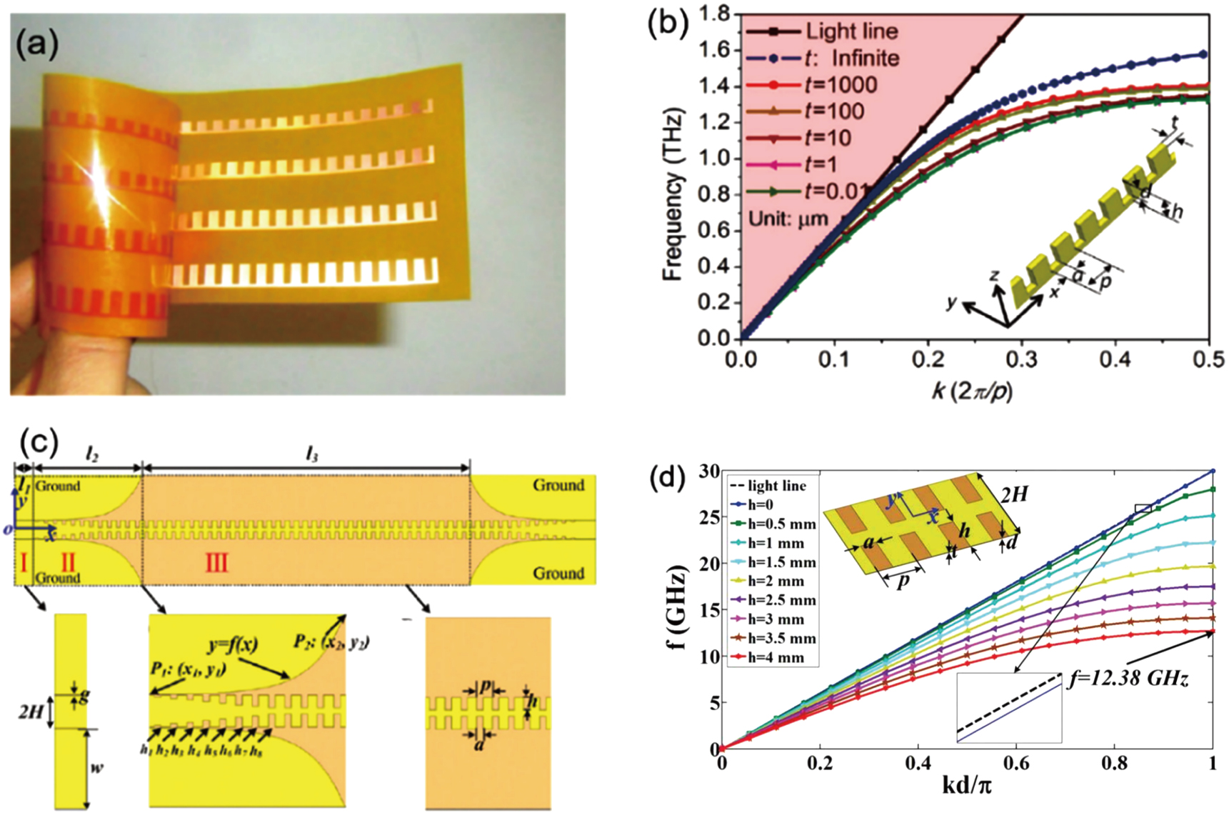
So far, several metamaterials have been designed to support spoof SPPs, such as periodically corrugated metal structures[68,69] and Domino structures.[70] To realize highly-integrated SPP waveguides and components, Cui et al. proposed ultrathin periodically corrugated metal strips, which support the spoof SPPs, as shown in Fig. 9(a).[71–73] The dispersion curves of the TM-polarized waves propagating along the corrugated metal strips were calculated by full-wave finite-element method simulations, as shown in Fig. 9(b).[72] It can be seen clearly that the dispersion curve gradually deviates from the light line as the thickness decreases, indicating that the thinner the corrugated metal strip, the stronger the confinement of the surface waves. Similarly to natural SPPs, there is a serious disagreement between the wavevector of the spoof SPPs and that in free space (k > k0) as well. Typically, the spoof SPPs on this corrugated metal strip can be efficiently launched by designing a matching transition bridge between the conventional coplanar waveguide (CPW) and the plasmonic waveguide.[74] As shown in Fig. 9(c), three functional modules were designed. The first module was a CPW (with an impedance of 50 Ω), supporting the quasi-transverse electric and magnetic modes with wave vector k0. The third module was the corrugated metal strip supporting the spoof SPP mode with wavevector k. In module II, a matching transition bridge consisting of a flaring ground and gradient grooves was designed. As can be seen in Fig. 9(d), the dispersion curve of the spoof SPPs is highly dependent on the groove depth. When the groove depth decreases from 4 mm to 0 mm, the wavevector of the spoof SPPs gradually approaches the wavevector in vacuum. Thus, the gradient groove structure can realize momentum matching from the CPW (k0) to the corrugated metallic strip (k). The flaring ground was used to confine the guided waves to improve the transmission efficiency. The reflection efficiency can be as low as −10 dB by using the transition bridge for this hybrid waveguide. Based on the excellent propagation characteristics of the spoof SPPs, such as subwavelength confinement, loss-less, and flexible dispersion properties, several plasmonic components have been developed to exploit their significant potentials in modern integrated circuits.[75–78] In Section 4, simple plasmonic circuits based on the spoof SPP waveguides are reviewed, such as the Y-shaped beam splitter and frequency splitter.
Fig. 9. (color online) (a) Photograph of the corrugated metal strip fabricated using a flexible copper clad laminate. (b) Dispersion curves of the spoof SPPs in the corrugated metal strips with different thicknesses (t). The black curve describes the light in free space, reproduced from Ref. [72]. (c) Configuration of the CPWs-to-spoof SPPs converter. I: CPW section. II: Matching transition bridge consisting of gradient grooves and a flaring ground. III: Spoof SPP waveguide (ultrathin corrugated metallic strip). (d) Dispersion curves of the ultrathin corrugated metallic strip (t = 18 μm) with different groove depths (h). The black curve describes the light in free space, reproduced from Ref. [74].
3.2. Bottom-up fabricated plasmonic waveguides
The bottom-up strategy attempts to build nanostructures from atomic or molecular components, referring mainly to the chemical synthesis. The first reported synthesis of plasmonic metal nanoparticles was performed more than 150 years ago when Faraday prepared Au colloids by reducing Au chloride with phosphorus in solution.[79] The performance of these chemically synthesized metal nanostructures is generally determined by a complex interaction of kinetics and thermodynamics.[80] Recently, shape-controlled synthesis has been accomplished by adding selective capping agents, which can change the order of facets free energies and drive the growth of the nanostructure to the expected shapes, such as sphere,[81] polyhedron,[82] or rod.[83] In this section, we focus on the review of chemically synthesized nanowires and nanobelts, which can perform as excellent plasmonic waveguides.
3.2.1. Nanowires
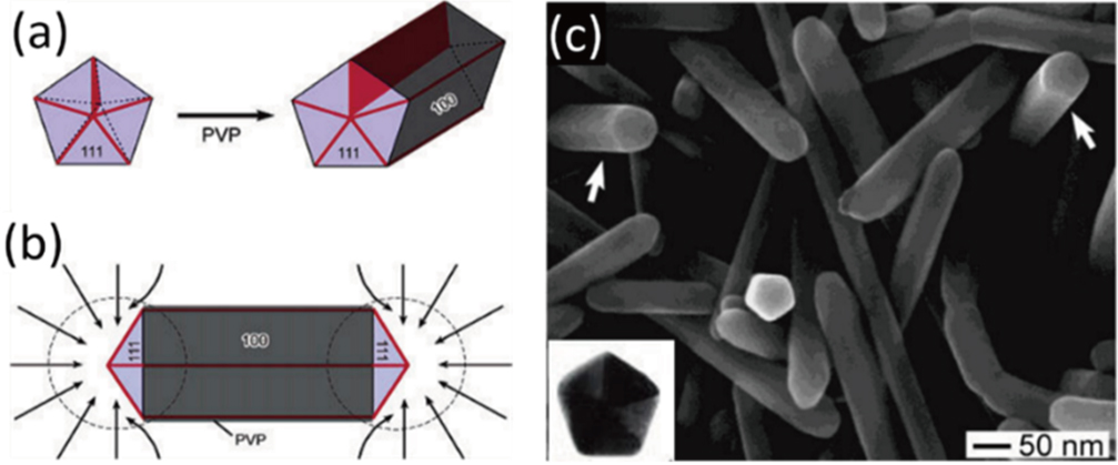
Comparing with the top-down fabricated waveguides, chemically synthesized metal nanowires can guide SPPs at visible regions with a significantly lower propagating loss owing to their unique single crystalline structure and atomically smooth surface. A convenient method to synthesize metal nanowires is to use a polyol process using poly(vinylpyrrolidone) (PVP) as the coordination reagent.[84] The PVP molecules can selectively cover the {100} facets and allow the {111} facets grow preferentially; thus, forming a one-dimensional nanowire structure (Fig. 10(a)). The yield, diameter, and aspect ratio of the nanowires can be controlled by tuning the experimental parameters, such as the molecular weight of the PVP and the molar ratio of its repeating unit relative to silver nitrate, temperature, injection rates, and reaction time. Figure 10(b) shows a typical scanning electron microscope (SEM) image of the as-synthesized Ag nanowires. The clear pentagonal cross sections further confirm the evolution of the nanowires from multiply twinned nanoparticles via anisotropic growth.
Fig. 10. (color online) Mechanism of nanowire synthesis. (a) Evolution of a nanowire from a multiply twinned nanoparticle. The ends of this nanowire are terminated by {111} facets and the side surfaces are bounded by {100} facets. (b) Diffusion of silver atoms toward the ends of the nanowire, with the side surfaces completely passivated by the PVP. (c) SEM images of the silver nanowires. The inset is a TEM image of the nanowire cross section, reproduced from Ref. [84].
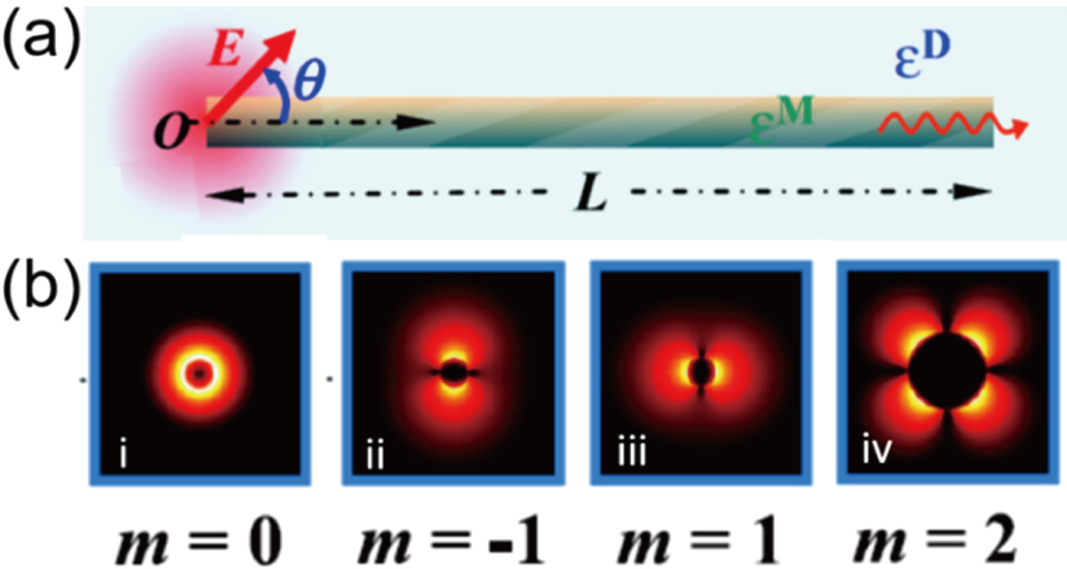
On the synthesized nanowire, multiple SPP modes with different propagation characteristics can be launched. For a cylindrical metal nanowire model, the electric field of the different plasmon modes can be written in cylindrical coordinates as
where m is the azimuthal quantum number, the SPPs propagate along the z-direction, and Em(r) is the radial distribution, expressed by Bessel functions. For nanowires with diameters less than 400 nm, the three lowest-order SPP modes, including TM0 (m = 0), HE−1 (m = −1), and HE1 (m = 1) modes, become dominant.[85–87] The field distributions of these SPP modes are shown in Fig. 11(b). Under a proper excitation polarization, these SPP modes can be launched simultaneously, which results in the interference of modes with amplitudes depending on the ratio of the diameter of the nanowire to the incident wavelength. Accordingly, Zhang et al. discussed the construction of chiral SPPs on a silver nanowire by the superposing two degenerate HE1 modes with a π/2 phase delay and an additional TM0 mode., The chiral SPPs can be studied by quantum dots fluorescence imaging, as shown in Fig. 12(a).[85] The maximum of the degree of chirality can be found at 45° and −45° excitation polarizations, corresponding to left-handed and right-handed SPPs, respectively. These results show that nanowires can be used as broadband, subwavelength circular polarized optical sources, which enables new methods for the chiral interaction with molecules at nanoscale. It is reported that the Raman optical activity (ROA) of chiral molecules can be effectively excited by chiral SPPs propagating on the nanowire,[88] as shown in Fig. 12(b). More details of the applications of nanowire modes interference are presented in Section 4.
Fig. 11. (color online) (a) Schematic illustration of an SPP propagating on a nanowire. The excitation beam with electric field E and polarization angle θ is focused on the nanowire end. (b) Field distribution of the four lowest-order SPP modes propagating on the nanowires, reproduced from Ref. [85].
Fig. 12. (color online) (a) Fluorescence images of SPPs propagating on a Ag nanowire. (i) Optical image of the nanowire. (ii)–(iv) Polarization-dependent fluorescence images of the SPPs, reproduced from Ref. [85]. (b) SEM image of Ag nanowires. (c), (d) Raman imaging of the structure in (b) with left circular polarization (c) and right circular polarization (d), reproduced from Ref. [88].
Owing to the atomically smooth surface and well-crystalline structure, the scattering loss and ohmic damping of the propagating SPPs can be greatly reduced and the LSPP on the synthesized nanowires can reach up to tens of micrometers. These robustly propagating SPPs can be reflected effectively by the wire end faces, and the interference between the incident and reflected SPPs can create a standing surface plasmon wave along the nanowire axis, indicating that the metal nanowires can be used as an SPP Fabry–Pérot resonator. Krenn et al. reported an SPP Fabry–Pérot resonator of synthesized nanowires first.[89] They investigated non-radiating surface plasmon modes on silver nanowires by SNOM mapping, with wavelengths shortened to approximately half of the exciting light, as shown in Fig. 13(c). It was reported that the propagation lengths can reach up to 10μm under an excitation of 785 nm, while the end face reflectivity was ∼25%. Resonator modes, i.e., standing surface plasmon waves along the nanowire axis, arise whenever an integer of half the surface plasmon wavelength is equal to the wire length. These results reveal that the near-field modulations of surface plasmons along the nanowire are due to the reflection of the SPPs at the wire termination.
Fig. 13. (color online) (a) Illumination of optical excitation: I denotes the input and D is the other end of the wire. (b) Optical image: the bright spot on the left is the focused exciting light. The arrow indicates the light scattered from the wire end. (c) SNOM image of the SPPs on a nanowire excited by 785 nm. (d) Cross-cut along the chain dotted line in (c), reproduced from Ref. [89]. (e) SEM image of a silver nanowire on a monolayer MoS2. (f) Magnified SHG image at the overlap region when the SPPs on the nanowire are excited at the left end. (g) Calculated SHG intensity at a plane located 1.3 μm from the monolayer MoS2. The scale bar is 2 μm in (e) and 500 nm in (f) and (g). (h) Intensity profiles along the Ag nanowire, corresponding to the dashed lines in (f) and (g), respectively, reproduced from Ref. [90].
Recently, Xu et al. discussed the second harmonic generation (SHG) excitation of monolayer molybdenum disulfide (MoS2) by Fabry–Pérot SPP resonance.[90] In general, it is difficult to enhance nonlinear optical processes using SPPs in plasmonic waveguides due to the mismatch in momenta. However, the parallel momentum of the propagating SPPs on the nanowires can vanish as the counter of incident and reflected SPPs, which allows the matching of momenta between the SHG photons and the SPPs. It was demonstrated that the generated SHG signals were emitted in the direction perpendicular to the nanowires. Figure 13(e) shows the compound structure of a silver nanowire on a monolayer MoS2. The SHG signals can only be measured in the overlapping region between the nanowire and MoS2, as shown in Fig. 13(f) (experiment) and Fig. 13(g) (simulation). The line intensity profile of the SHG signal (Fig. 13(h)) shows that the Fabry–Pérot resonance of the SPPs modulates the SHG of the monolayer MoS2, which results in a regular beating pattern observed in the far-field SHG image at the overlapping region.
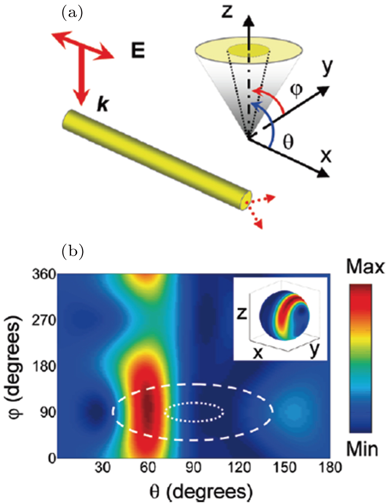
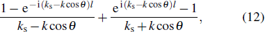
The Fabry–Pérot nature of the SPPs propagating on the nanowire can highly affect the direction of the emission of the SPPs at the wire ends. Li et al. measured the spatial distribution of the nanowire emission for the first time.[38] By gradually varying the numerical aperture (N.A.) of the objective, the intensity containing the direction information of the emission of the SPPs can be detected. As shown in Fig. 14(a), the N.A. of the objective can be tuned in the range of 0.5–1.2. Under this configuration, only the emission within the collection cone can be detected; thus the measured intensity becomes a function of the N.A. of the objective. Figure 14(b) shows the emission distribution as a function of angles ϕ and θ, which are the azimuthal and polar angles, respectively, defined in the inset. It was found that the emission from the nanowire termination peaked at an angle θ ≃ 60°. This emission is the result of the superposition of two counter-propagating dipole currents. The forward and backward traveling current can be expressed as
where I0 is the amplitude of the current, ks is the wavevector of the propagated surface plasmons in the wire, and z is the coordinate in the direction of the wire. The superimposed radiation of the two moving current elements is
where l is the length of the current element and k is the wavevector of the light under dielectric circumstances.
Fig. 14. (color online) (a) Referred coordinates. The wavevector and polarization of the excitation light are represented by the red arrows. The N.A. corresponds to the opening angles of the collection cone. The emission from the wire end is collected by an objective. (b) Calculated emission intensity as a function of angles ϕ and θ. The inset shows the corresponding angular distribution on the integration sphere, reproduced from Ref. [38].
3.2.2. Nanobelts
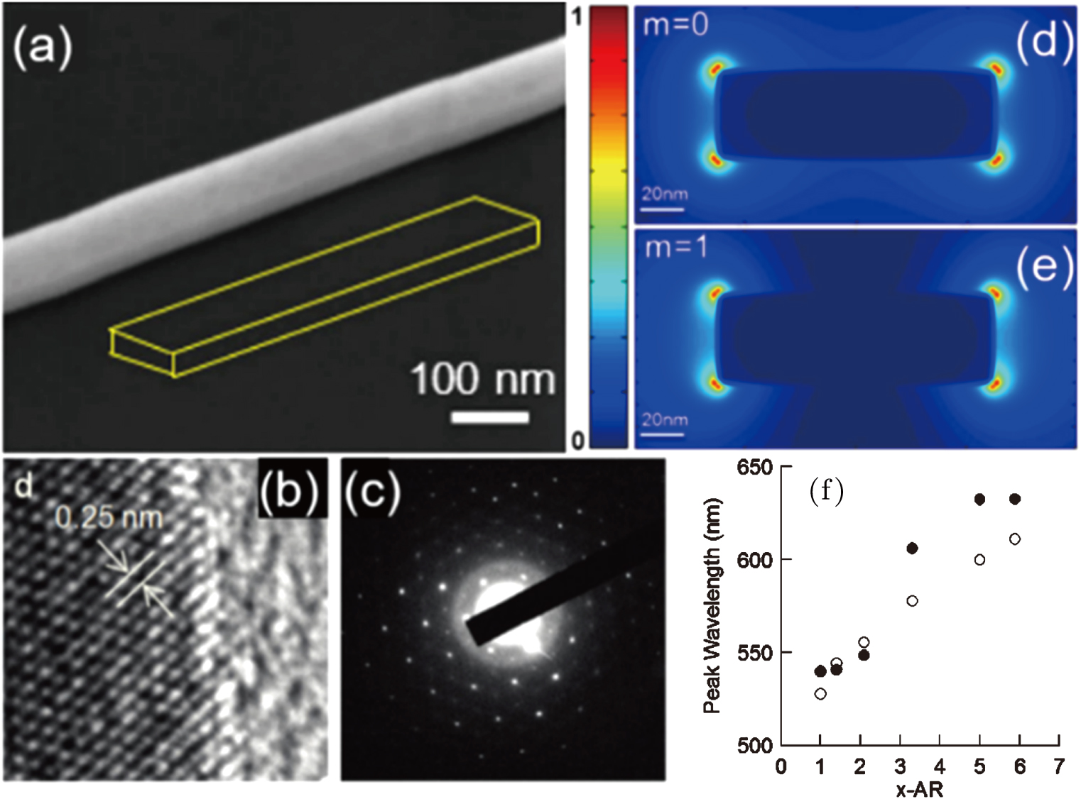
Synthesized metal nanobelt structures, similarly to the nanowires with rectangular cross section, can also be used as excellent plasmonic waveguides. Qi et al. reported gold nanobelt synthesis with a surfactant mixture of cetyltrimethylammonium bromide (CTAB) and sodium dodecyl sulphate (SDS).[91] It was revealed by SEM, high-resolution TEM, and diffraction pattern measurements (Figs. 15(a)–15(c)), that the synthesized nanobelt exhibited a single-crystalline structure, which grows along the ⟨211⟩ direction and has a {111} plane on the top flat surface. Figures 15(d) and 15(e) show the near-field distribution of the two lower-order SPP modes (m = 0 and m = 1) propagating along the nanobelt. Compared with nanowires, nanobelts can provide a higher-level confinement of the SPPs, while inevitably suffer from larger propagation loss. However, it is reported that a weakly excited antisymmetric mode (m = 1) can have a long propagation length with a strong confinement. By the excitation of SPPs by low coherence LED light, a propagation length greater than 10 μm can be measured.[92] Interestingly, the transverse surface plasmon resonance of nanobelts can be flexibly tuned by varying the aspect ratio of the cross section, which cannot be realized on nanowires. The resonance peak can shift from 525 nm to 625 nm when the aspect ratio of the cross section is changed from 1 to 5 (Fig. 15(f)).[93] This phenomenon implies that nanobelts with a length of tens of micrometers can be used as flexible plasmonic waveguides, which can have a great advantage in the applications of biological sensing or detection.
Fig. 15. (color online) (a) SEM image of a gold nanobelt. The sample was tilted by 45° to reveal the rectangular cross section. (b) High-resolution crystalline structure of the nanobelt. (c) Electron diffraction indicates the single-crystalline gold structure, reproduced from Ref. [91]. (d)–(e) Calculated field intensity of a 125 nm × 40 nm gold nanobelt for the m = 0 (d) and m = 1 (e) modes, reproduced from Ref. [92]. (f) SPP scattering peaks at different cross section aspect ratios in experiments (black) and simulations (white), reproduced from Ref. [93].
4. Applications of SPP waveguides
SPP waveguides exhibit a unique capacity to concentrate and manipulate light in deep subwavelength regions, which makes them particularly useful for the future design and development of integrated nanophotonic devices and circuits. In the following section, certain functional plasmonic components and devices, which have been developed with SPP waveguides, are introduced.
4.1. Sensors
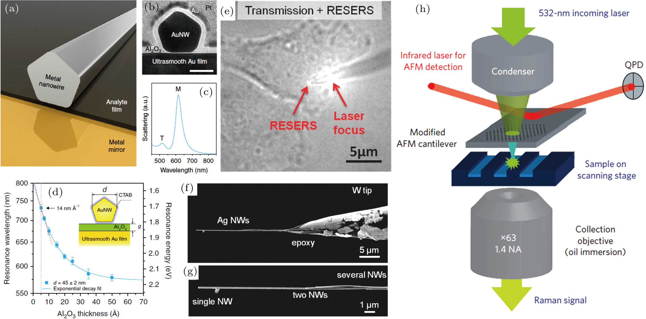
As it is well known, the LSPR frequency strongly depends on the size and shape of the particles and the dielectric constant of the surrounding medium.[94–96] By varying these parameters, the resonances can be tuned over the visible and mid-infrared regions. Thus, the LSPR of metal nanostructures can be used as an effective sensor, as it has been demonstrated in such promising applications as chemical identification[97–99] or biological detection.[100–102] Compared with nanoparticles, SPP waveguides can be used as a sensor with several unique advantages, which cannot be achieved simply by LSPR; thus, it has been attracting increasing attention in recent years. A typical advantage is that the larger scattering cross section provided by the waveguides can allow ultrasensitive detection of the changes in the environment, especially with some SPP cavity modes confined in a deep nanoscale area. Xu et al. recently reported the sensing of vertical dimensional variations by a nanowire-on-mirror system.[103] The structures are shown in Figs. 16(a) and 16(b). By tracking the spectral shift of the cavity–plasmon resonance, the thermal expansion of the layer within the gap between the nanowire and the mirror can be detected with a differential resolution of 0.58 pm. The shifting of the resonant peak with the variation of the thickness of the Al2O3 at the gap region is shown in Fig. 16(d). In addition, the system can also be used to track minute changes in humidity, which indicates that the nanowire sensor can be used for gas detection.
Fig. 16. (color online) (a) Coupled metal nanowire and mirror system. The change in thickness of the separating layer can be precisely detected. (b) High-resolution TEM image of the cross section of the nanowire and mirror system. The scale bar is 30 nm. (c) Calculated scattering spectrum of a 45-nm-diameter Au nanowire on a gold film with 2 nm separation. (d) Measured resonant peak of the cavity plasmon mode as a function of the Al2O3 layer thickness, reproduced from Ref. [103]. (e) Remote excitation SERS of a live HeLa cell by Ag nanowire. (f) SEM image of a typical tungsten tip with Ag nanowires attached. (g) Magnified image of the probe tip, reproduced from Ref. [104]. (h) Schematic of the experimental setup, showing the integration of the nanofocusing remote SERS sensor into an AFM microscopy, reproduced from Ref. [105].
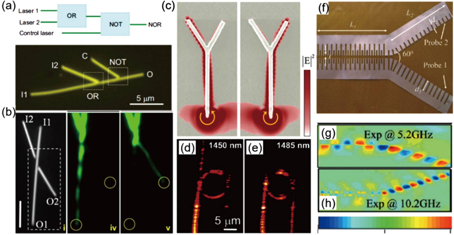
Fig. 17. (color online) (a) Nanowire networks as an optical logic gate. Diagram of a NOR logic gate built using cascaded OR and NOT gates (upper) and optical image of the designed structure (lower), reproduced from Ref. [107]. (b) (i) Optical image of a nanowire network with two input terminals (I1 and I2) and two output terminals (O1 and O2). (ii) and (iii) QD fluorescence images for two phase differences corresponding to the strongest output at terminal O1 and O2, respectively, reproduced from Ref. [108]. (c) SPP router by SOI of light, reproduced from Ref. [109]. (d) and(e) SPP wave router using V-groove, reproduced from Ref. [64]. (f) Image of a spoof SPP router. (g) and (h) Spoof SPP field measured on the router of (f), reproduced from Ref. [76].
Nevertheless, the SPP waveguides can support remote chemical sensing, which can prevent any modification or destruction to the analytes by direct illuminations, especially in living systems. Uji-i et al. recently reported a living cell remote-excitation surface-enhanced Raman scattering (SERS) detection by a nanowire-nanoparticle coupling system (Fig. 16(e)).[104] The nanowire, attached on a tungsten tip can be freely manipulated, as shown in Figs. 16(f) and 16(e). To use the nanowire as probe, different areas of the cell can be detected with high spatial resolution and lower photodegradation, compared with conventional local SERS. Remote chemical sensing by plasmonic waveguides can also be realized on noncoupling geometries. Large SERS enhancement can be generated at the apex of the tapered waveguides by the nanofocusing effect of tapered nanostructures; thus, the remote signal can be detected around the apex region. Figure 16(h) shows a nanofocusing remote-excitation SERS detection system, where a metal cone is fabricated as a nanofocusing remote-excitation source.[105] Combined with AFM microscopy, the chemical information of the sample surface can be mapped. With this device, topographic and chemical information imaging can be obtained simultaneously with a spatial resolution of ∼ 7 nm.
4.2. Routers
For an integrated plasmonic chip with both electronic and SPP components, a router is necessary as a BUS to process the signals. In an electronic circuit, besides the on and off states, a third state of no input is needed, so that the signals can be exchanged without being disturbed by other components. As metal nanowires can simultaneously support different SPP wavelengths and can manipulate them independently, they become suitable choices for a router in plasmonic circuits.[106] In particular, by changing the polarizations of the excitation light, the mode components and field distributions on the nanowires can be manipulated, as discussed in Section 3, which provides a method to control the routing of plasmons in the nanowire networks (Fig. 17(a)).
An SPP router with a nanowire network can be implemented by employing the varied phase difference of SPP modes interference.[107,108] As shown in Fig. 17(b), the SPPs are launched at two input ends (at I1 and I2), and the plasmon routing can be determined between two output ends (at O1 and O2). The plasmon energy can be routed to the O1 terminal for certain input phases. By changing the excitation polarization at the input ends, the phase difference can be increased, which results in the transferring of energy from the O1 to the O2 terminal. Quantum dot (QD) fluorescence images show that the intensity of the signal on the two branches of the outputs switches between strong and weak in an alternating way, determining the switching of the output intensity at the two output terminals O1 and O2 (Fig. 17(b)). As a result, this simple four-terminal nanowire network can function as a binary half adder by defining a threshold intensity for the “1” and “0” states. In addition, an SPP router can also be achieved by the nanowire spin–orbit interaction (SOI) effect, where the excitation is approached using an excitation source with a circular polarization.[109] The SPPs can be routed by changing the chirality of the excitation polarization as shown in Fig. 17(c). Another frequency router has also been achieved by CPP waveguides, such as a metal V-groove.[63,64] CPP-based components can be characterized in the wavelength range of 1425–1600 nm. As shown in Figs. 17(d) and 17(e), CPP ring waveguides can be used as a frequency router with a wavelength selectivity of ∼ 40 nm. In addition, a frequency router can also be realized by periodically corrugated metal strips supporting spoof SPPs.[76] As can be seen in Fig. 17(g), for such frequency splitter, the spoof SPP fields at the low (5.2 GHz) and high (10.2 GHz) frequency bands can be guided to probe 1 branch and probe 2 branch, respectively.
4.3. Modulators
A broad dynamic range of light absorption in the plasmonic structures opens the possibility for the efficient all-optical modulation of SPP transmission. Recently, for planar nanostructures, electro-optical modulation light transmission by a multimode interference in a plasmonic waveguide has been realized.[110,111] However, in the above examples, the modulation was achieved using planar SPP modes, which are less confined in the lateral direction and cannot realize a high-degree on-chip integration.
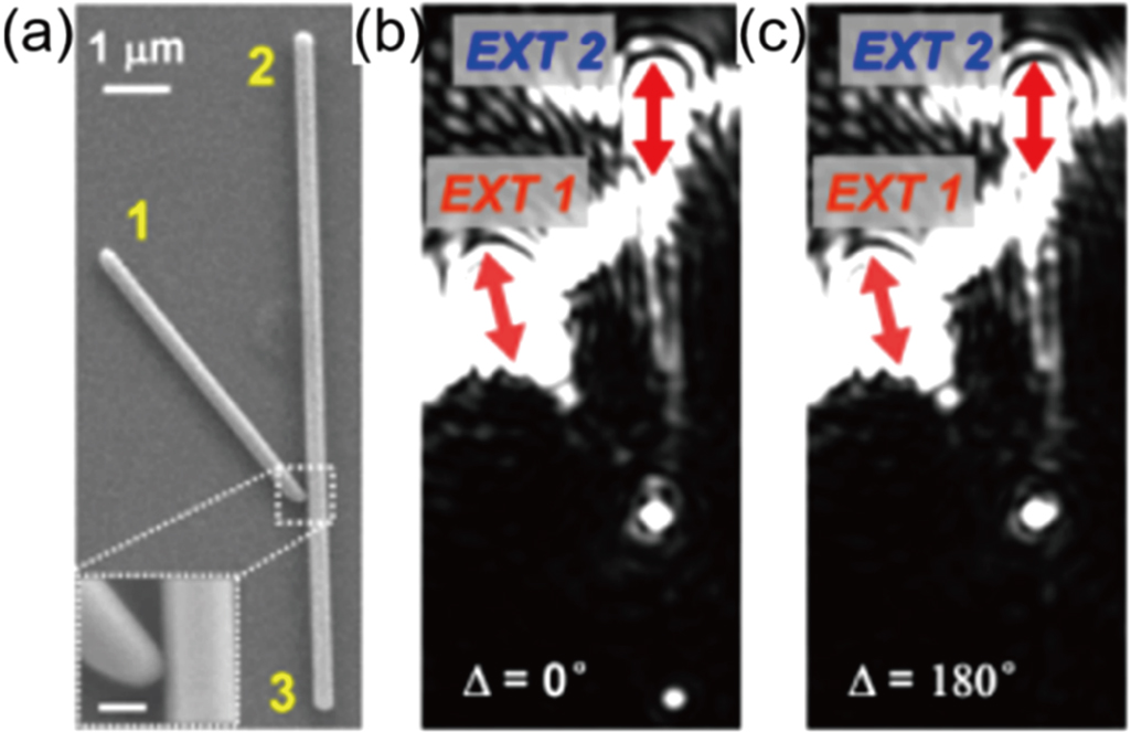
Recently, Li et al. reported that a highly-confined SPP modulator can be implemented using nanowire structures.[112] Figure 18(a) shows an interference based all-optical nanowire modulator. The device consists of two nanowires, forming a “y” structure. The two adjacent arms of the structure, 1 and 2, function as input ends, and the remaining end of the longer wire, 3, functions as the output. By changing the relative phase or the relative polarization angle of the two input signals, constructive and destructive interferences of the plasmons launched on the main wire arise, resulting in a strongly modulated emission of the signal at the output (see Figs. 18(b) and 18(c)). Owing to the confinement of the SPP modes on the modulator, the device can be directly coupled to other plasmonic components in integrated circuits.
Fig. 18. (color online) (a) SEM image of a nanowire structure as SPP modulator. (b) and (c) Optical images of the branch excited by two coherent 633-nm laser spots at inputs 1 and 2, respectively. The phase difference of the two SPPs at output 3 is Δ = 0°(b) and 180°(c), reproduced from Ref. [112].
5. Conclusion and outlook
In summary, we briefly reviewed the characteristics of various SPP waveguides operating in visible, infrared, and terahertz regimes. The dispersion relation reveals that the SPP wavevector is larger than that of free space light at the same frequency, which permits the subwavelength confinement beyond the diffraction limit. So far, various plasmonic waveguides have been fabricated by top-down and bottom-up methods, such as metal stripes, grooves, nanowires, and periodically corrugated surface, which can be crucial building-blocks to construct next-generation photonic devices with high-density integration. Certain simple plasmonic devices and circuits have been accomplished for applications, such as ultrasensitive sensing, BUS router, or light intensity modulation. In spite of the advancement in the research of functional elements, there are still several difficulties restraining the achievement of nanophotonic devices and circuits for real applications, such as the issues about the trade-off between the propagation length and confinement, bending loss, and the interface between the plasmonic and electronic circuits. With the further development of nanofabrication techniques, we can anticipate highly-integrated plasmonic circuits, which can be used for practical information transmission and processing, to be available in the near future.
Surface plasmon polariton waveguides with subwavelength confinement*
Project supported by the National Natural Science Foundation of China (Grant Nos. 11704266 and 11774245), the Fok Ying Tung Education Foundation, China (Grant No. 151010), the Scientific Research Base Development Program of Beijing Municipal Commission of Education, China, the General Foundation of Beijing Municipal Commission of Education, China (Grant No. KM201810028006), and the Training Program of the Major Research Plan of Capital Normal University, China.
[Yang Longkun1, Li Pan1, Wang Hancong2, Li Zhipeng1, †]


