† Corresponding author. E-mail:
Project supported by the National Key R&D Program of China (Grant No. 2018YFA0208402), the National Basic Research Program of China (Grant No. 2012CB932302), the National Natural Science Foundation of China (Grant Nos. 11634014, 51172271, and 51372269), the Strategic Priority Research Program of the Chinese Academy of Sciences (Grant No. XDA09040202).
Solar cells that combine single-crystalline silicon (Si) with graphene (G) have been widely researched in order to develop next-generation photovoltaic devices. However, the power conversion efficiency (PCE) of G/Si solar cell without chemical doping is commonly low due to the relatively high resistance of graphene. In this work, through combining graphene with carbon nanotube (CNT) networks, we fabricated three kinds of hybrid nanocarbon film/Si heterojunction solar cells in order to increase the PCE of the graphene based Si solar cell. We investigated the characteristics of different nanocarbon film/Si solar cells and found that their performance depends on the heterojunctions. Specifically, a doping-free G-CNT/Si solar cell demonstrated a high PCE of 7.9%, which is nearly equal to the combined value of two individuals (G/Si and CNT/Si). This high efficiency is attributed to the synergistic effect of graphene and CNTs, and can be further increased to 9.1% after applying a PMMA antireflection coating. This study provides a potential way to further improve the Si based heterojunction solar cells.
Graphene (G), an atomically thick two-dimensional nanocarbon material, has attracted increasing attention in the development of next-generation photovoltaic devices due to its excellent electrical, optical, and chemical stable properties.[1–6] In particular, solar cells that combine crystalline silicon (Si) with graphene synthesized by the chemical vapor deposition (CVD) method have shown promising potential because of the simple and low-cost fabrication process.[7–9] In a typical G/Si heterojunction solar cell, the graphene film not only participates in the formation of the heterojunction, but also serves as the window electrode and hole collector.[9–11] When the device is illuminated, the incident light passes through the graphene and creates electron–hole pairs in the Si substrate.[12] The generated electron–hole pairs are then separated by the built-in electric field. Afterwards, the separated holes diffuse across the graphene film in the lateral direction to be collected. Hence, good transparency and conductivity of the graphene film are of high importance to obtain the expected solar cell with high power conversion efficiency (PCE).
However, due to the polycrystalline feature of CVD-graphene and cracks or residues formed in the polymer-assisted transfer processes, the obtained graphene films commonly show relatively high sheet resistance in the range of several hundreds to thousands of Ω/sq.[13–18] When applied in the Si solar cells, the high sheet resistance of graphene not only causes severely charged carrier recombination, but also brings about serious power loss. For instance, Ho et al.[15] reported that the relatively low conductivity of graphene (990 Ω/sq) leads to a low fill factor (FF) of the G/Si solar cell, which results in a low PCE of 3.3%. Similarly, a G/Si solar cell with a PCE of 3.47% was also reported based on graphene with sheet resistance of 1500 Ω/sq.[16] Chemical doping of graphene can yield enhanced FF and open circuit voltage of the G/Si solar cells.[11,14,19] However, the doped solar cells face the problem of fast degradation,[9] which greatly influences their developments.
Recently, many studies have focused on the assembly of graphene with carbon nanotube (CNT), which yields new types of nanocarbon materials with diverse structure characteristics and different properties.[20–24] On the one hand, high strength one-dimensional CNTs can reinforce the atomically thin graphene film, which is conductive to the polymer-free transfer process.[21] On the other hand, the hybrid films of graphene and CNTs have shown better conductivity compared to an individual graphene or CNT film, making them more adoptable for flexible transparent conductive electrodes.[18,22,23] Apart from the hybrid films, the native oxides on Si have also been proved to greatly affect the characteristics of as fabricated heterojunction solar cells by controlling the magnitude of the thermionic emission dark current.[14,25] However, the optimal oxides for different heterojunctions require different thicknesses.[26–28] Our previous report has also shown that, in a PEDOT:PSS-CNT/Si solar cell, the optimal oxide thickness between PEDOT:PSS/Si heterojunction is thinner compared to that of CNTs/Si, which brings about the difficulty in the design of an oxide layer to fulfill the needs for both PEDOT:PSS and CNT based Si solar cells.[29] Considering the similar sp2 hybridization structure and properties of graphene and CNTs, their optimal oxide thicknesses are almost the same. These features provide a lot of convenience for us to construct the high efficiency Si solar cells based on graphene and CNTs.
In this work, we improved the G/Si solar cell efficiency through hybridizing graphene with CNTs and investigated the performance of the hybrid films with diverse assembly configurations in Si solar cells. Specifically, three types of hybrid films based on graphene and CNT network were assembled, including G/CNT and CNT/G hybrid films, which were fabricated by simple stacking CNT network on graphene, as well as a coplanar nanostructure (G-CNT film) synthesized by a chemical vapor deposition (CVD) method. We found that the solar cell performance depends on the nanocarbon/Si heterojunction. The G-CNT/Si solar cell, in which there are both G/Si and CNT/Si contact heterojunctions, exhibits better J–V characteristics than the ones with a single type of contact. Its high efficiency (PCE = 7.9%) is attributed to the synergistic effect of graphene and CNTs. After applying a PMMA antireflection coating, the PCE of the as-fabricated PMMA/G-CNT/Si solar cell can be further improved to 9.1%. These findings illustrate the dependence of the Si solar cell performance on different nanocarbon materials and provide a potential way to further enhance the efficiency of this type of solar cells.
Graphene film was grown by Cu-catalyzed low-pressure chemical vapor deposition (LPCVD) method using H2 and CH4.[30] The Cu foil (46365, from Alfa Aesar) was first treated with ammonium persulfate to remove the native oxides, then cleaned with acetone, ethanol, and deionized water successively. The cleaned Cu foil was then loaded into a quartz tube and the system was pumped to vacuum. Then the tube was put inside a furnace and heated to 1020 °C in the atmosphere of H2 (15 sccm). Next, 1 sccm CH4 was introduced with the H2 gas flow rate unchanged. After 10 min growth, the furnace was turned off and the quartz tube was cooled down to ambient temperature.
To assemble the CNT/G hybrid film, a transparent and conductive freestanding CNT network film, in which the CNT bundles are interconnected well with each other by Y-type junctions, was transferred onto the graphene/Cu substrate.[31] Then a drop of ethanol was used to enhance the contact of CNTs and graphene. After drying, the Cu substrate was dissolved in the ammonium persulfate solution, leaving a free standing CNT-G hybrid film. To obtain the G/CNT hybrid film, the CNT/G hybrid film was carefully flipped over to the other side.
The preparation process of the coplanar G-CNT hybrid film is similar to that employed in an earlier report.[32] A piece of continuous CNT network was first transferred onto a pretreated Cu foil (46365, from Alfa Aesar), then placed in the quartz tube and the quartz tube was evacuated. The following procedures are the same as the growth procedures of graphene described above. The sample was then taken out from the quartz tube and floated on the ammonium persulfate solution to dissolve Cu. Finally, a G-CNT hybrid film floated on the solution was obtained.
N-type silicon wafer (100) with resistivity of 1–3 Ω·cm and 300 nm SiO2 were used to fabricate solar cells. The wafer was first patterned to square windows by ultraviolet photolithography and the exposed SiO2 was etched in BOE solution, leaving a bare fresh Si surface (3 mm × 3 mm). After that, the Si substrate was washed with acetone and ethanol for several times. To obtain an optimal oxide layer, the Si substrate was immersed in dilute nitric acid (0.5 M) for 40 s. Different nanocarbon materials were then transferred onto the substrates to form different junctions. Afterwards, silver paste was painted around the active window while eutectic gallium-indium (EGaIn, from Alfa Aesar) was applied to the back side of Si to form the cathode.
Raman spectra were recorded using LabRAM HR 800 (HORIBA Jobin Yvon Inc.) with a 514 nm laser. An atomic force microscope (AFM, Bruker MultiMode-8 ScanAsyst) was used to characterize the surface morphology of different nanocarbon materials. The optical transmission was measured with a Shimadzu UV-3600 UV–Vis–NIR spectrophotometer. A handheld four-probe meter (Tonghui, TH2661) was used to measure the sheet resistance of different nanocarbon materials. The performance of a solar cell was measured using a solar simulator (Perfectlight CHF-XM 500) under AM 1.5 G with a calibrated irradiation intensity of 100 mW/cm2. The J–V data were recorded with a Keithley 4200-SCS.
Figure
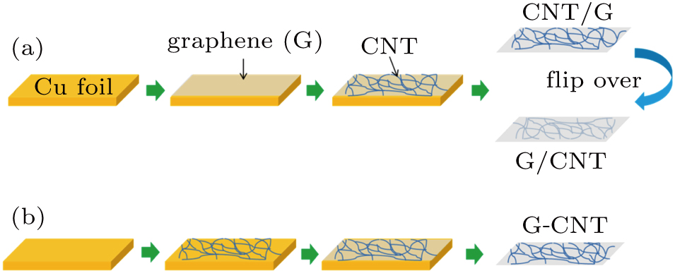 | Fig. 1. (color online) Schematic fabrication processes of graphene and CNT based hybrid films with different configurations: (a) CNT/G and G/CNT hybrid films, (b) coplanar G-CNT hybrid film. |
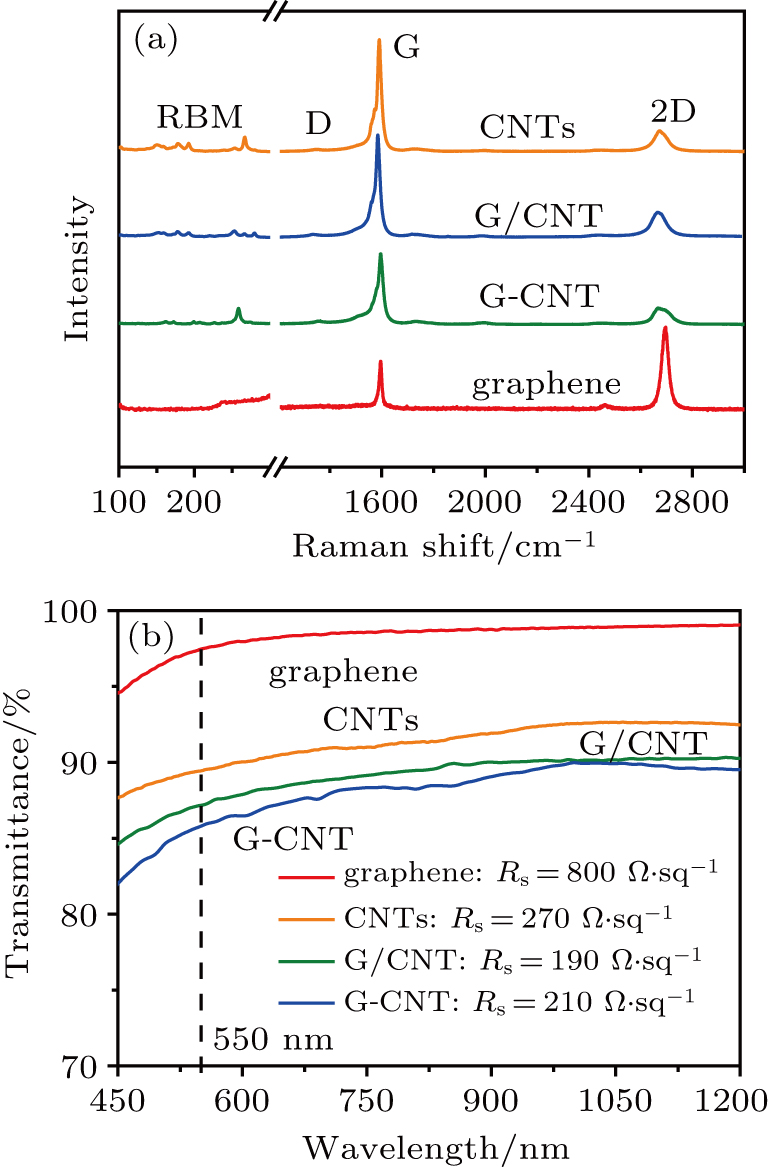
In the Raman spectra of different nanocarbon materials, as shown in Fig.
Figure
From the surface morphology of each hybrid film on a SiO2 (300 nm)/Si substrate characterized by AFM (Fig.
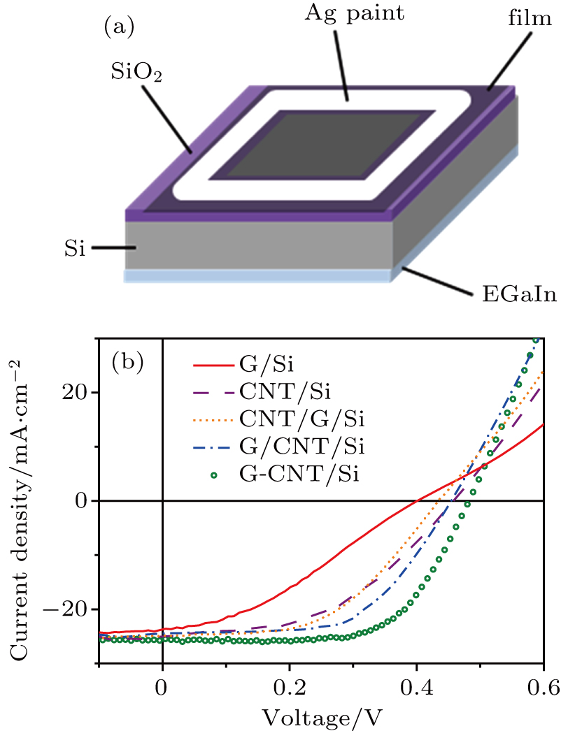
In order to investigate the performance of different nanocarbon films applied in Si based solar cells, the films were transferred onto n-type single crystalline Si substrates to form heterojunctions (junction area is 9 mm2 for all devices). The structure of the as-designed nanocarbon film/Si heterojunction solar cell is depicted in Fig.
| Table 1. Comparison of device parameters of different Si based heterojunction solar cells with graphene, CNT network, G/CNT, CNT/G, and G-CNT hybrid films as the top electrodes. . |
Furthermore, the series resistance (Rs) and ideality factor (n) are calculated under the dark measurements with the following equation:[14]
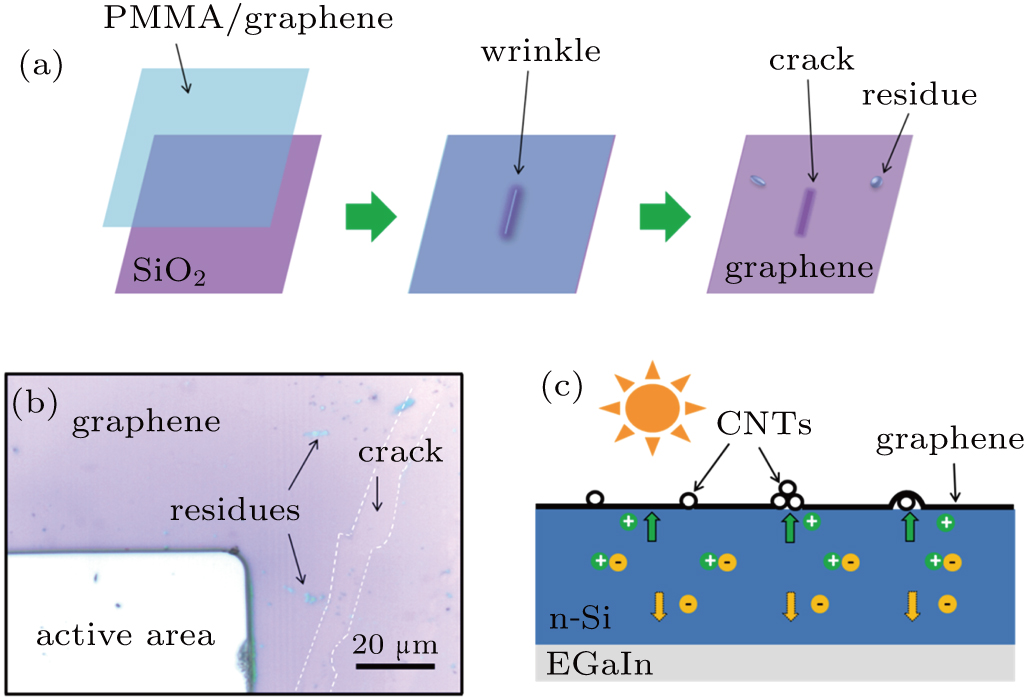
In fact, the majority of reported graphene grown by the CVD method shows a sheet resistance of about 1000 Ω/sq, which is much larger than its theoretical value (30 Ω/sq).[34] Unlike the freestanding CNT network, the graphene grown on copper catalyst substrate needs to be protected in the course of transfer. The commonly used method is spin coating a thin PMMA layer on the graphene to serve as a protective sacrifice layer.[30] However, cracks and polymer residues are often formed in this process (Fig.
Interestingly, the PCE of the G-CNT/Si solar cell is higher than that of the G/CNT/Si and CNT/G/Si solar cells. As the sheet resistance and optical transmittance of these hybrid films are almost the same, the only difference is the heterojunction formed with Si. For the G/CNT or CNT/G hybrid films, there only exists one type of heterojunction (G/Si heterojunction or CNT/Si heterojunction). However, because of the hybridization method employed for the hybrid films, the graphene and CNTs contact the Si together in the G-CNT/Si solar cell, jointly forming two types of heterojunctions, as shown in Fig.
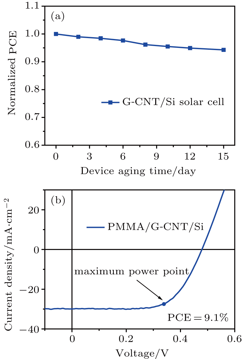
The stability of the G-CNT/Si solar cell is further studied (Fig.
We have analyzed the characteristics of doping-free G/Si solar cells and found that the relatively poor performance results from the high resistance of the CVD-derived graphene film. Through the introduction of a continuous and conductive CNT network, we designed three types of hybrids with different configurations, which all showed much better conductivity than graphene. As a result, a Si solar cell with a high and stable PCE of 7.9% without chemical doping was fabricated based on a coplanar G-CNT hybrid film. The PCE was improved by about 46% and 139% compared to those of the individual CNT/Si (5.4%) and G/Si (3.3%) solar cells fabricated at the same condition. By investigating the characteristics of different nanocarbon film/Si solar cells, we revealed the dependence of their performance on the heterojunctions formed in the devices. On the one hand, the efficiency improvement of the G-CNT/Si solar cell is attributed to the same optimal interfacial oxide thickness of G/Si heterojunction and CNT/Si heterojunction, which makes it feasible to obtain optimal heterojunction quality simultaneously. On the other hand, the coexistence of G/Si and CNT/Si heterojunctions in the G-CNT/Si photovoltaic device exhibits a synergistic effect, resulting in more carrier transport paths and more efficient carrier collection. Finally, the device efficiency was further enhanced to 9.1% after applying a PMMA antireflection coating. Our work also reveals new aspects of the device architecture and the potential for Si based heterojunction photovoltaic devices.
| [1] | |
| [2] | |
| [3] | |
| [4] | |
| [5] | |
| [6] | |
| [7] | |
| [8] | |
| [9] | |
| [10] | |
| [11] | |
| [12] | |
| [13] | |
| [14] | |
| [15] | |
| [16] | |
| [17] | |
| [18] | |
| [19] | |
| [20] | |
| [21] | |
| [22] | |
| [23] | |
| [24] | |
| [25] | |
| [26] | |
| [27] | |
| [28] | |
| [29] | |
| [30] | |
| [31] | |
| [32] | |
| [33] | |
| [34] | |
| [35] | |
| [36] |


