Degradation of current–voltage and low frequency noise characteristics under negative bias illumination stress in InZnO thin film transistors*

Project supported by the Opening Fund of Key Laboratory of Silicon Device Technology, Chinese Academy of Sciences (Grant No. KLSDTJJ2018-6), the National Natural Science Foundation of China (Grant No. 61574048), the Science and Technology Research Project of Guangdong Province, China (Grant No. 2015B090912002), and the Pearl River S & T Nova Program of Guangzhou City, China (Grant No. 201710010172).

Wang Li1, 2, 3, Liu Yuan1, 2, 3, †, Geng Kui-Wei1, Chen Ya-Yi1, 2, En Yun-Fei2
School of Electronic and Information Engineering, South China University of Technology, Guangzhou 510640, China
Science and Technology on Reliability Physics and Application of Electronic Component Laboratory, CEPREI, Guangzhou 510610, China
Key Laboratory of Silicon Device Technology, Chinese Academy of Sciences, Beijing 100029, China


† Corresponding author. E-mail: Liuyuan@ceprei.com

Project supported by the Opening Fund of Key Laboratory of Silicon Device Technology, Chinese Academy of Sciences (Grant No. KLSDTJJ2018-6), the National Natural Science Foundation of China (Grant No. 61574048), the Science and Technology Research Project of Guangdong Province, China (Grant No. 2015B090912002), and the Pearl River S & T Nova Program of Guangzhou City, China (Grant No. 201710010172).

Abstract

The instabilities of indium–zinc oxide thin film transistors under bias and/or illumination stress are studied in this paper. Firstly, illumination experiments are performed, which indicates the variations of current–voltage characteristics and electrical parameters (such as threshold voltage and sub-threshold swing) are dominated by the stress-induced ionized oxygen vacancies and acceptor-like states. The dependence of degradation on light wavelength is also investigated. More negative shift of threshold voltage and greater sub-threshold swing are observed with the decrease of light wavelength. Subsequently, a negative bias illumination stress experiment is carried out. The degradation of the device is aggravated due to the decrease of recombination effects between ionized oxygen vacancies and free carriers. Moreover, the contributions of ionized oxygen vacancies and acceptor-like states are separated by using the mid-gap method. In addition, ionized oxygen vacancies are partially recombined at room temperature and fully recombined at high temperature. Finally, low-frequency noise is measured before and after negative bias illumination stress. Experimental results show few variations of the oxide trapped charges are generated during stress, which is consistent with the proposed mechanism.

1. Introduction

Due to its excellent electrical performance and good stability,[1] the amorphous indium zinc oxide thin film transistor (a-IZO TFT) is drawing a great deal of attention in the next generation of active matrix liquid crystal displays (AMLCD) and active matrix organic light emitting diodes (AMOLED).[2] During its application, the device may be exposed to variable environments, such as illumination, temperature, humidity, etc. As reported in Refs. [3]–[6], the electrical characteristics and the typical parameters of IZO TFTs may change in the above environments, which may further influence the performances of the image capture and display system. Moreover, IZO TFTs may be simultaneously subjected to diverse stresses. In particular, the degradation of the device under bias illumination stress may be more serious and thus it should be investigated before its application in the consumer market.

The instability of TFT under illumination and/or gate bias stress has been studied by many groups.[714] As reported, the notable degradations of current–voltage (IV) and capacitance–voltage (CV) characteristics have been studied under the above bias illumination stress.[12,13] These degeneration phenomena can be attributed to the formation of localized states and the fixed oxide trapped charges.[10,12] The formation of localized states mainly arises from the generation of ionized oxygen vacancies in the channel while the formation of oxide trapped charges is due to the occupation of neutral traps in the gate oxide.[13,14] However, few papers have reported the low frequency noise (LFN) characteristics of IZO TFTs after negative bias illumination stress (NBIS). The low frequency noise of the devices may limit the minimum signal level that can be correctly detected by the subsequent circuit. Moreover, the low frequency noise may be up-converted into phase noise and high frequency noise in some conditions, which may affect the linearly of an analog circuit.[15] Thus, the noise performance of IZO TFT needs to be analyzed and minimized.

Flicker (1/f) noise is a random fluctuation phenomenon in a semiconductor device and it is sensitive to semiconductor quality and device defects. As a non-destructive reliability characterization method, 1/f noise measurement has been widely used in the evaluation and selection of BJT, MOS, GaN, semiconductor lasers, and other devices.[16] In addition, the energy and spatial distribution of traps can be extracted and the degeneracy of the devices can be analyzed by 1/f noise.

In this paper, a series of experiments is performed to study the stabilities of IZO TFTs under illumination and/or electrical stress. The dependence of degradation characteristics on the illumination wavelength is also analyzed. The contributions of stresses induced ionized oxide vacancies ( ) and acceptor-like states are separated. Furthermore, the LFN is measured before and after NBIS. The concentrations of traps near the IZO/SiO2 interface are extracted and the spatial distributions of trapped charges in the gate oxide are calculated.

2. Device performance and low frequency noise measurement
2.1. Devices structure and IV characteristics

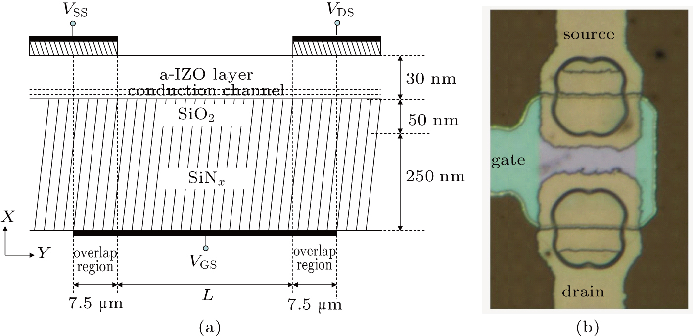
The device under test is IZO TFT with bottom gate structure as shown in Fig. 1. A 300-nm-thick layer of aluminum gate was sputtered and patterned by wet etching. Then, the insulating layer, including 50 nm of SiO2 and 250 nm of SiNx, was deposited by plasma-enhanced chemical vapor deposition (PECVD) at 310 °C. Subsequently, an IZO layer of 30 nm was deposited by radio frequency magnetron sputtering. A stacked structure of molybdenum/aluminum/molybdenum (25 nm/100 nm/25 nm), used as source and drain electrodes, was formed via sputtering and patterned by lift-off technology, which controls the channel length and width. Finally, the device was passivized by a 300-nm-thick SiO2 layer grown by PECVD.[17] In experiment, all devices had the same channel width/length i.e., 20 μm/10 μm, specifically. The measured unit area gate oxide capacitance (Cox) was about 14.1 nF.

Fig. 1. (color online) (a) Cross-sectional view and (b) micrograph of IZO TFT.

The transfer characteristics of the device are shown in Fig. 2. The calculated threshold voltage (Vth) is about 4.35 V, the field effect mobility (μFE) is about 25.62 cm2·V−1·s−1, and sub-threshold swing (SS) is about 0.4 V/dec. It was reported in Refs. [18] and [19] that the oxygen vacancies (Vo) act as the dominant native point defects in metal oxide. The transition level from +2 to 0 is close to the conduction band minimum (CBM), the ionized Vo is a shallow donor and thus gives rise to the n-type conductivity in metal oxide.

Fig. 2. (color online) Transfer characteristics in the IZO TFT under different values of VDS.

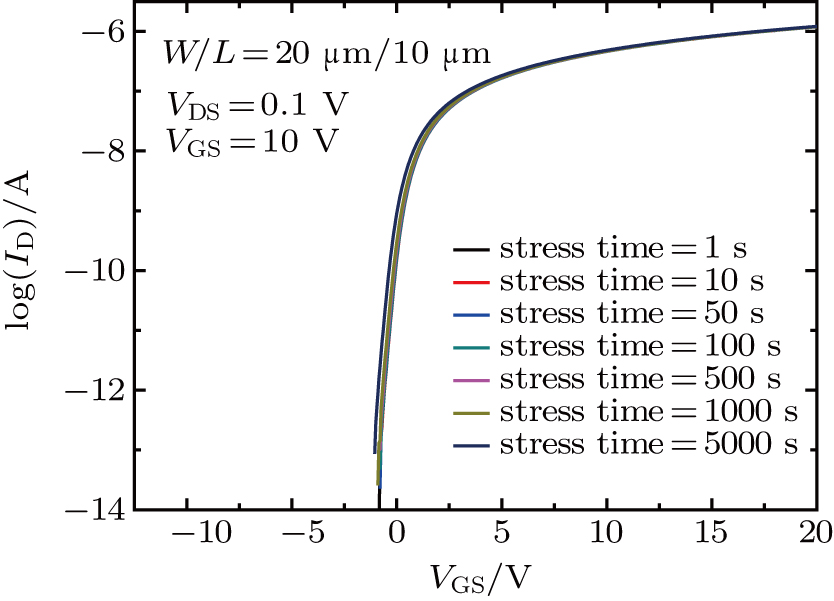
Good stability of IZO TFT is shown in this experiment. The measured transfer curves of the device under NBS stress with VGS = −10 V are plotted in Fig. 3. Indistinguishable variations of transfer characteristics are observed with the increase of stress time. In oxide thin film transistors, the density of deep states in the bottom half of the band-gap is approximately 5 × 1020 cm−3.[20] Therefore, the Fermi level is pinned at deep levels and few holes may accumulate in the channel with a negative voltage. Thus, a small fraction of accumulated holes may inject into the gate oxide and less variation of Vth can be observed.

Fig. 3. (color online) Variations of transfer curves under different negative bias stresses (VGS = −10 V).
2.2. Low frequency noise measurement

The measurement setup of drain current noise power spectra of IZO TFTs is illustrated in Fig. 4.[21] The electrical properties of IZO TFTs were measured by an Agilent B1500. The ADQ214 was used to measure the noise power spectral density of the device. The Keysight E4727A was adopted to construct the filter and amplifier units of the noise test system. The matching resistance RG and RD were selected by waferpro based on the bias condition.

Fig. 4. Measurement setup of low frequency noise in IZO TFT.
3. Illumination induced degradation in IZO TFT

In this section, a series of illumination experiments were performed. The degradations of IZO TFTs under monochromatic illumination were studied. The dependence of degradation characteristic on wavelength was then analyzed. In this experiment, the used light intensity was 5 mW/cm2 and wavelengths were 635 nm, 515 nm, 450 nm, and 405 nm.

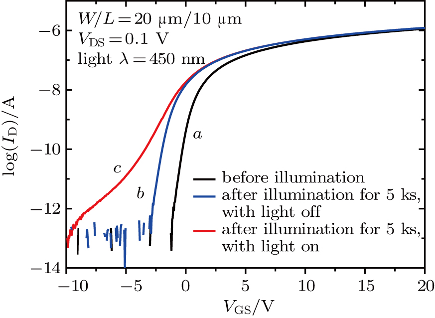
Transfer characteristics of IZO TFTs exposed to blue laser light (λ = 450 nm) are shown in Fig. 5. The photon energy of blue light in this experiment was about 2.8 eV calculated by the Planck equation:

h is the Planck constant, and its value is 4.14 × 10⁻¹⁵ eV; c is the speed of light in a vacuum; λ is the wavelength that corresponds to the light energy. As shown in Fig. 5, a parallel negative shift of the transfer characteristic after illumination (curve b) is found compared with that before illumination (curve a). The calculated Vth varies from 4.34 V to 3.15 V while few variations of sub-threshold swing are observed. Furthermore, larger sub-threshold current and sub-threshold swing are observed under illumination (curve c) than that measured in the dark (curve b).

Fig. 5. (color online) Plots of IV characteristic curves of IZO TFTs under blue illumination.

As reported in Ref. [22], donor-like states and acceptor-like states may exist in the channel. The donor-like states are neutral because the occupied electrons and positive are neutralized while being emptied. The negative shift of IV characteristic curve after illumination may relate to donor-like states (oxygen vacancies, Vo.[13] As reported in Refs. [23]–[25], a large number of Vo exist on the top of the valence band. The Fermi level in the IZO/SiO2 interface lowers nearly to midgap in a case with applying negative gate voltage. Therefore, oxygen vacancies can be photo-excited and become . These become stable due to outward relaxations of neighboring metal atoms after long time illumination. Therefore, the generated deep-level may act as positive fixed charges existing near the IZO/SiO2 interface, which effectively screen the gate bias and then result in related negative shifts of IV curves as shown in Fig. 5. However, there are also the latest reports[18,19] indicating that the oxygen vacancies exist near the conduction band minimum rather than what the traditional opinion says, specifically oxygen vacancies are at a deep level. The Vo is +2 charged near the CBM, which may influence the IZO TFT stability under stress (especially temperature). The stability of the device is affected by the decrease of the oxygen vacancy defects, which are located near CBM when annealed at above the crystallization temperature.

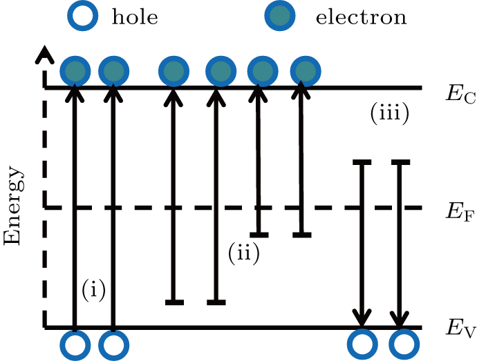
The notable sub-threshold currents observed under illumination are due to the optically generated free carriers. As shown in Fig. 6, the optically generated carriers may relate to three main mechanisms during light exposure. (i) Electrons are directly excited from the valence band to the conduction band. (ii) Electrons in deep level traps of band-gap are excited to the conduction band, which is accompanied by the generation of sub-gap states. (iii) Holes in traps above Fermi level of the band gap are excited to the valence band with defects generated at the same time. In this experiment, the photon energy of blue light is less than the band gap of a-IZO layer and mechanism (i) may not happen. In addition, the density of holes in the upper half of the band gap is very low and mechanism (iii) may not dominate. Therefore, the optically generated carriers may dominate by mechanism (ii), which relates to free electrons excited from Vo and acceptor-like states below the Fermi level. As reported in Ref. [24], the sub-threshold swing only relates to the density of acceptor-like deep states. As shown in Fig. 5, the sub-threshold swing becomes larger during illumination and quickly recovers in the dark. This phenomenon indicates that the excess sub-threshold current may dominate by the excitation process of electrons from acceptor-like states below the Fermi level.

Fig. 6. (color online) Generating mechanism of free carriers under blue illumination.

The plots of log(ID) versus VGS in the IZO TFTs with the illumination of four different wavelengths are shown in Fig. 7. Like the above discussion, the sub-threshold current increases with the decrease of wavelength, which is also caused by photo-generated electrons released by acceptor-like deep states and donor-like states under illumination. As shown in the inset of Fig. 7, more negative shifts of Vth are observed in the range of wavelength from 625 nm to 405 nm. This phenomenon indicates that may be generated by photon excitation with the photon energy increasing.

Fig. 7. (color online) Transfer characteristics under long time illumination (5000 s) with four wavelengths.
4. Instabilities under negative bias illumination stress
4.1. Degradation of IV characteristics

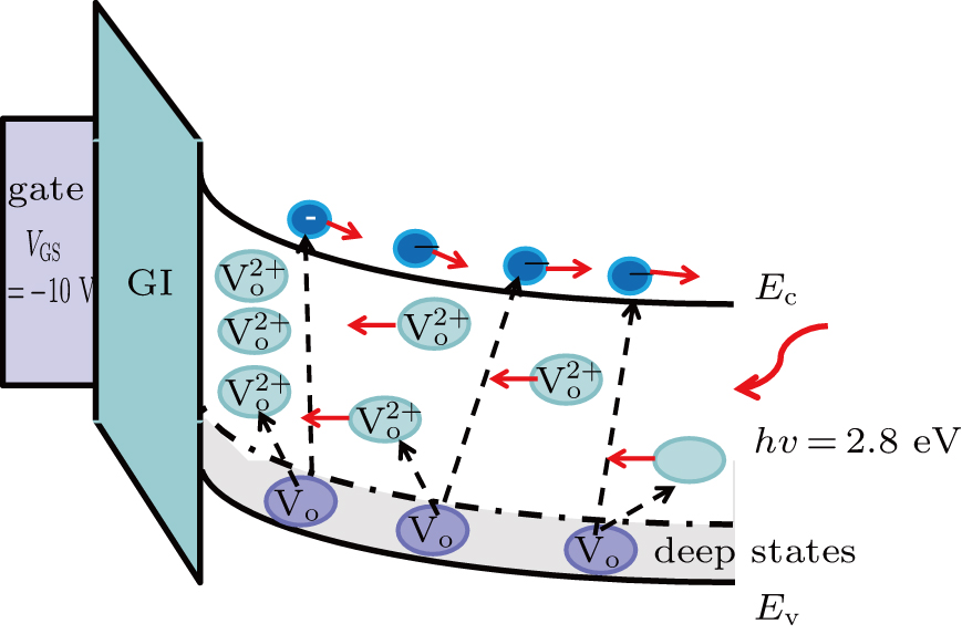
Figure 8 shows the measured transfer characteristics of IZO TFTs during NBIS when VGS is about −10 V and the light wavelength is about 450 nm.[26,27] The energy of the selected wavelength needs to be greater than the ionization energy of oxygen vacancy and smaller than the band gap of IZO. The value of ΔVth after stress is about −3.15 V, which is more serious than that measured under the illumination stress. The sub-threshold swing is also varied from 0.4 V/dec to 1.7 V/dec, which may be due to the change of acceptor-like states. As reported in Ref. [28], the degradation induced by NBIS can also be explained by the oxygen vacancy model, which is shown in Fig. 9. The electrons are swept from the IZO/SiO2 interface to the back IZO/passivation interface under an applied negative gate voltage. In addition, can also be moved and accumulated in the IZO/SiO2 interface.[13,29] Since the electrons in the IZO/SiO2 interface are depleted, the recombination effect between and electrons strongly decrease during stress. Thus, more are formed, and greater degradation of Vth is observed.

Fig. 8. (color online) Transfer curves of IZO TFT, measured under different illumination stress times.
Fig. 9. (color online) Oxygen vacancy model under NBIS.

The variation of the threshold voltage during stress may simultaneously be affected by photo-generated ionized oxygen vacancies (with surface density Qov = qΔNov) and the generation of acceptor-like deep states in the IZO/SiO2 interface (with surface density Qdeep = qΔNdeep), and it can be expressed as[30]

The values of ΔVov and ΔVdeep can be extracted using the procedure proposed by McWhorter and Winokur,[31] the acceptor-like deep states are neutral at the midgap, and only the oxygen vacancies can affect the shift of midgap voltage as given as
The VMG is the gate voltage at which the sub-threshold current flows under the midgap condition. Since the device is of an amorphous semiconductor, the sub-threshold current in the VMG can be expressed as[31]

Here, μn is the electron mobility at room temperature, ε0 is the vacuum dielectric constant, ni is the carrier concentration at room temperature, and the value of φs at the midgap is 0. The value of sub-threshold current, calculated in VMG is about 3.88 × 10⁻¹⁰ A, which can be used to extract the value of ΔVMG. Then, the number of oxygen vacancies can also be extracted by using the midgap voltage. According to Eq. (2), ΔNdeep can be extracted from the experimental threshold voltage (ΔVth) and the calculated number of oxygen vacancies (ΔVov).

The extracted variations of oxygen vacancies and acceptor-like states in the channel layer are plotted in Fig. 10. It is obviously shown that the shift of threshold voltage is dominated by ionized oxygen vacancies, which causes the negative shift of Vth. Since the electrons at the interface are depleted, more may accumulate near the interface and be fixed. In addition, the generation of acceptor-like states not only causes the threshold voltage to shift toward positive but also increases the sub-threshold swing as shown in Fig. 10.

Fig. 10. (color online) Separations of stress induced ionized oxygen vacancies and acceptor-like states.
4.2. Annealing characteristic after negative bias illumination stress

The annealing characteristics of IZO TFTs after NBIS are graphed in Fig. 11. The extracted values of ΔVth in stress and annealing process are shown in Fig. 12. In the annealing process, the two-phase annealing phenomenon is present. An instant recovery may happen at the end of the stress, and then recovery of the device tends to be saturated. As described above, the variation of Vth is mainly caused by the ionized oxygen vacancies. Therefore, the phenomenon indicates that the partially unstable are recombined with the electrons immediately at the end of the stress and the relatively stable can keep fixed at the IZO/SiO2 interface. As shown in Fig. 11, the device does not recover to the initial states after 20 h at room temperature. The stable may be formed due to the outward relaxation and metal atoms moving to positions far away from their initial positions. The above stable cannot be easily recovered at room temperature. However, the device characteristics can fully resume to the initial state and the crystal structure is not changed by annealing in the air (The annealing atmospheres have no effect on the device stability due to the 300-nm passivation layer on the surface of the device.[32]) for 10 h at 120 °C, which indicates that those stable can be recovered after obtaining enough external energy.

Fig. 11. (color online) Annealing characteristics under different NBIS conditions.
Fig. 12. Extracted ΔVth versus stress time in stress and annealing process.
4.3. LFN characteristics before and after NBIS

The curves of measured normalized drain current power spectral densities versus drain current before and after stress are shown in Fig. 13. According to the carrier number fluctuation model, the normalized current spectral density of IZO TFTs can be expressed as[33]

where gm is the device transconductance, SVfb is the flat-band voltage spectral density, Nt is the trap concentration, and λ is the tunneling attenuation coefficient, which is about 0.1 nm for SiO2.[34]

Fig. 13. (color online) Curves of normalized noise versus drain current power spectral density after NBIS.

Based on Fig. 13, the flat-band voltage spectral densities can be extracted to be about 1.37 × 10⁹ V2·Hz−1 and 1.53 × 10⁹ V2·Hz−1, respectively. According to Eq. (5), the extracted Nt values are about 8.18 × 1017 cm−3·eV−1 before NBIS and about 9.14 × 1017 cm−3·eV−1 after NBIS, respectively. As reported in Ref. [35], the noise spectrum originated from carriers exchanging between the channel and traps in the gate dielectric. The low frequency noise further reveals that the total of localized states and trapped charges in the gate insulator increases after NIBS.

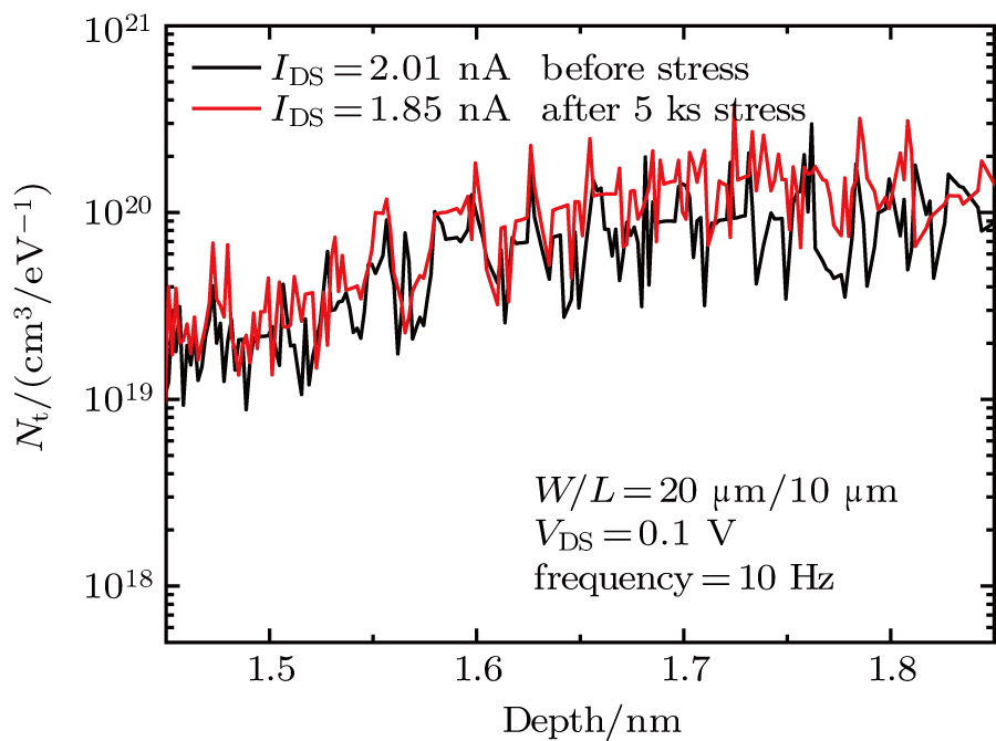
In order to have a qualitative spatial distribution of trapped charges in the gate oxide, the frequency is converted into the tunneling depth as follows:[3639]

where τ0 is the time constant at the IZO/SiO2 interface, x is the distance from the interface to the gate oxide, αt is the tunneling attenuation coefficient, which is about 108 cm−1 for SiO2. The value of τ0 is equal to 10−10 s for traps distributed near the interface. Equation (6) states that the probability of penetration into the gate oxide decreases exponentially with distance. The extracted density profiles of trapped charges before and after stress are shown in Fig. 14. Negligible shifts of defect space distribution curves before and after stress can be observed, which indicates that few trapped charges are formed during stress, which is consistent with the theory discussed in the above section. This phenomenon also verifies that the NBIS effect of IZO TFTs may be dominated by ionized oxygen vacancies at the IZO/SiO2 interface.

Fig. 14. (color online) Spatial distributions of oxide trapped charge density in gate oxide before and after stress.
5. Conclusions

Instability of IZO TFT under negative bias illumination stress has been discussed in this paper. The degradation effects of IZO TFT may be dominated by ionized oxygen vacancies. More negative shifts of threshold voltage under illumination can be observed with the decrease of light wavelength. Furthermore, electrons captured by acceptor-like states below Fermi-level may be photo-excited and thus lead to the increase of sub-threshold current and sub-threshold swing. In addition, LFN measurement is performed before and after negative bias illumination stress separately. Indistinguishable variation in spatial distribution of oxide trapped charges is observed after stress, which is consistent with the proposed degradation mechanism.

Reference
[1] Lan L Xiong N Xiao P Li M Xu H Yao R Wen S Peng J 2013 Appl. Phys. Lett. 102 242102
[2] Fortunato E Barquinha P Martins R 2012 Adv. Mater. 24 2945
[3] Lee K H Ji S J Son K S Park J S 2009 Appl. Phys. Lett. 95 1309
[4] Tang L F Lu H Ren F 2016 Chin. Phys. Lett. 33 038502
[5] Huang X Wu C Lu H Ren F 2012 Appl. Phys. Lett. 100 243505
[6] Chang G W Chang T C Jhu J C Tsai T M 2014 IEEE Electron. Dev. Lett. 61 2119
[7] Nomura K Kamiya T Hirano M Hosono H 2009 Appl. Phys. Lett. 95 013502
[8] Chowdhury M D H Migliorato P Jang J 2011 Appl. Phys. Lett. 98 153511
[9] Chowdhury M D H Ryu S H Migliorato P Jang J 2011 J. Appl. Phys. 110 114503
[10] Chen T C Chang T C Hsieh T Y Tsai C T Chen S C Lin C S Jian F Y Tsai M Y 2011 Thin Solid Films 520 1422
[11] Nomura K Kamiya T Hosono H 2011 Appl. Phys. Lett. 99 488
[12] Gwang Um J Mativenga M Migliorato P Jang J 2012 Appl. Phys. Lett. 101 468
[13] Oh H Yoon S Ryu M K Hwang C Yang S Park S K 2010 Appl. Phys. Lett. 97 488
[14] Migliorato P Md D H C Gwang Um J Seok M 2012 Appl. Phys. Lett. 101 2945
[15] Tseng Y C Huang W M Spears E Spooner D Ngo D Ford J M 2002 IEEE Electron Dev. Lett. 20 54
[16] Fung T C Baek G Kanicki J 2010 J. Appl. Phys. 108 074518
[17] Liu Y Chen R S Li B En Y F Chen Y Q 2018 IEEE Trans. Electron. Dev. 65 356
[18] Kim H Choi D Park S Park K Park H W Chung K B Kwon J Y 2017 Appl. Phys. Lett. 110 232104
[19] Liu L Mei Z Tang A Azarov A Kuznetsov K Xue Q K Du X 2016 Phys. Rev. 93 235305
[20] Nomura K Kamiya T Yanagi H Ikenaga E Yang K Kobayashi K Hirano M Hosono H 2008 Appl. Phys. Lett. 92 202117
[21] Fung T C Back G Kanicki 2010 J. Appl. Phys. 108 074518
[22] Billah M M Chowdhury M D H Mativenga M Um J G Mruthyunjaya R K Heiler G N 2016 IEEE Electron. Dev. Lett. 37 735
[23] Kamiya T Nomura K Hosono H 2009 Phys. Status Solidi 206 860
[24] Kamiya T Nomura K Hirano M Hosono H 2008 Phys. Status Solidi 5 3098
[25] Ryu B Noh H K Choi E A Chang K J 2010 Appl. Phys. Lett. 97 022108
[26] Ji K H Kim J I Jung H Y Park S Y Choi R Mo Y G Jeong J K 2011 Microelectronic Engineering 88 1412
[27] Kim J H Kim U K Chung Y J Ji S J et al. 2011 Appl. Phys. Lett. 98 488
[28] Kim Y Kim S Kim W Bae M Jeong H K Kong D Choi S Kim D M Kim D H 2012 IEEE Trans. Electron. Dev. 59 2699
[29] Nomura K Kamiya T Hosono H 2011 Appl. Phys. Lett. 99 053505
[30] McWhorter P J Winokur P S 1986 Appl. Phys. Lett. 48 133
[31] Kouvatsos D N Davidovic V Papaioannou G J Stojadinovic N Michalas L Exarchos M Voutsas A T Goustoridis D 2004 Microelectronics Reliability 44 1631
[32] Loannidis E G Tsormpatzoglou A Tassos D H 2010 J. Appl. Phys. 108 106103
[33] Chen W T Lo S Y Kao S C Zan H W Tsai C C Lin J H Fang C H Lee C C 2011 IEEE Electron. Dev. Lett. 32 1552
[34] Liu Y Wu W J Lei Qiang Wang L En Y F Li B 2015 Chin. Phys. Lett. 32 088506
[35] Hung K K Ko P K Hu C Cheng Y C 1990 IEEE Trans. Electron. Dev. 37 654
[36] Liu Y Wu W J Li B En Y F Wang L Liu Y R 2014 Acta Phys. Sin. 63 098503 in Chinese
[37] Ioannidis E G Tsormpatzoglou A Tassis D H Dimitriadis C A Templier F Kamarinos G 2010 J. Appl. Phys. 108 106103
[38] Tsormpatzoglou A As N Mahmoudabadi F Choi N Hatalis M K Dimitriadis C A 2013 IEEE Electron. Dev. Lett. 34 1403
[39] Liu Y Chen H B Liu Y R Wang X En Y F Li B Lu Y D 2015 Chin. Phys. 24 088503