Enhanced transient photovoltaic characteristics of core–shell ZnSe/ZnS/L-Cys quantum-dot-sensitized TiO2 thin-film*

Project supported by the Natural Science Foundation of Hebei Province, China (Grant Nos. E2013203296 and E2017203029).

Li Kui-Ying, Ren Lun, Shen Tong-De
State Key Laboratory of Metastable Materials Science & Technology, Yanshan University, Qinhuangdao 066004, China


† Corresponding author. E-mail: kuiyingli@ysu.edu.cn

Project supported by the Natural Science Foundation of Hebei Province, China (Grant Nos. E2013203296 and E2017203029).

Abstract

Photoanodic properties greatly determine the overall performance of quantum-dot-sensitized solar cells (QDSCs). In the present report, the microdynamic behaviors of carriers in the nanocomposite thin-film, a ZnSe QD-sensitized mesoporous La-doped nano-TiO2 thin-film, as a potential candidate for photoanode, are probed via nanosecond transient photovoltaic (TPV) spectroscopy. The results confirm that the L-Cys ligand has a dual function serving as a stabilizer and molecular linker. Large quantities of interface states are located at the energy level with a photoelectric threshold of 1.58 eV and a quantum well (QW) depth of 0.67 eV. This QW depth is approximately 0.14 eV deeper than the depth of QW buried in the ZnSe QDs, and a deeper QW results in a higher quantum confinement energy. A strong quantum confinement effect of the interface state may be responsible for the excellent TPV characteristics of the photoanode. For example, the peak intensity of the TPV response of the QD-sensitized thin-film lasts a long time, from 9.40 × 10⁻⁷ s to 2.96 × 10⁻⁴ s, and the end time of the PTV response of the QD-sensitized thin-film is extended by approximately an order of magnitude compared with those of the TiO2 substrate and the QDs. The TPV characteristics of the QD-sensitized thin-film change from p-type to n-type for the QDs before and after sensitizing. These properties strongly depend on the extended diffusion length of the photogenerated carries and the reduced recombination rate of photogenerated electron-hole pairs, resulting in prolonged carrier lifetime and an increased level of electron injection into the TiO2 thin-film substrate.

1. Introduction

In the past 20 years, quantum dots-sensitized solar cells (QDSCs) have aroused much scientific interest in the field of optical and solar energy.[13] Quantum-dot (QD) sensitizers possess unique properties, such as a multi-exciton effect, quantum confinement effect, high excitation coefficient, and low cost.[2] The theoretical conversion efficiency of a QDSC is much higher than those of silicon and dye-sensitized solar cells.[4] However, this high efficiency has not been experimentally achieved.[58] Thus, experimentally improving the efficiency is a challenge. In recent years, research on QDSCs has mainly concentrated on their photovoltaic conversion and electrochemical properties.[913] The study of the transport mechanism of photoinduced free charge carriers (FCCs) in the photoanode consisting of a wide bandgap semiconductor and QD sensitizer is important because the photoanode is a key component for determining the overall performance of QDSC.[1417] In the present paper, a mesoporous La-doped nano-TiO2 thin film is used as a substrate material of the photoanode because it has a direct wide bandgap of more than 3.0 eV. Some outstanding properties of the thin film material, such as a large specific surface area and porosity, competent skeleton structure, and particularly good photoelectric features of anatase titanium dioxide, were found in our previous studies.[18,19] In particular, self-assembled core–shell ZnSe/ZnS/L-Cys QDs, which were prepared at room temperature by an aqueous synthesis technique, show superior photoelectronic characteristics and low biotoxicity when compared with other nanocrystalline group II/IV semiconductors.[20,21] Therefore, the ZnSe QDs are used as a sensitizer for the photoanode in our experiments. Some scientific questions arise. How does an effective molecular link form between the ZnSe QDs and mesoporous TiO2 thin film? Does a more efficient transport channel exist for photoinduced FCCs? Additionally, what is the transport mechanism of photoinduced FCCs in the ZnSe QD-sensitized mesoporous nano-TiO2 thin film? Here, we intend to answer these questions experimentally using a chemical bath deposition (CBD) processing method, TPV and steady-state surface photovoltaic (SPV) techniques, Fourier transform infrared (FT-IR) spectroscopy and ultraviolet-visible (UV-VIS) absorption spectroscopy. Transient photovoltaic (TPV) spectroscopy is a non-invasive micro-test method, which is used for exploring microdynamic behaviors of FCCs in semiconductors, such as separation rate of electron-hole pairs and lifetime of FCCs.[22]

2. Experimental details
2.1. Nano-TiO2 thin film preparation

A mesoporous La-doped nano-TiO2 thin film was manufactured. Briefly, mesoporous La-doped TiO2 nanoparticles were prepared by sol–gel, a method in which polyethylene glycol (PEG) is used as a template.[21,23] Figure S1 in Appendix A shows the adsorption-desorption curves and distribution of the pore diameter of the prepared nano-TiO2. Then, the nano-TiO2 slurry was formed by adding both the as-prepared TiO2 nanoparticles and an appropriate quantity of α-turpentine into an ethyl cellulose ethanol solution. The slurry was dispersed under ultrasonication for 30 min and then exposed to air until achieving an appropriate viscosity. Fluorine-doped tin oxide (FTO) glass was coated with the prepared TiO2 slurry by knife coating.[24] The coated FTO glass was calcined at 500 °C for 0.5 h after drying at 60 °C for 2 h in air. The first layer of the mesoporous La-doped nano-TiO2 thin film was obtained. Multilayer films were obtained layer by layer in the same way. Figure S2 displays the x-ray diffraction patterns of the prepared nano-TiO2 powders and thin film. The thickness of each layer of the as-prepared substrate nano-TiO2 thin film, which was determined using a step measuring instrument, was approximately 3 μm as shown in Fig. S3 in Appendix A.

2.2. QD-sensitized nano-TiO2 thin film preparation

The ZnSe QD-sensitized mesoporous La-doped nano-TiO2 thin film was prepared by a CBD method.[25,26] Briefly, both selenium and zinc precursor solutions of the ZnSe QD sensitizer were prepared by using L-Cys as a ligand at room temperature.[20] The Se and Zn precursors were mixed in a volume ratio of 1 : 1. The as-prepared mesoporous La-doped nano-TiO2 thin film was first immersed in the mixed solution for a specific time at a given temperature. Then, the ZnSe QD-sensitized nano-TiO2 thin film was obtained after the cleaned thin film had been dried at 60 °C for 2 h.

2.3. Characterizations

The x-ray diffraction (XRD; Rigaku D/max-2500/PC, Japan) and high-resolution transmission electron microscopy (HRTEM; JEOL-2010 electron microscope, Tokyo, Japan) were used to study the crystal structures and the average particle size of QDs, respectively. Fourier transform infrared spectroscopy (EQYUBIX55; Bruker, Germany) was used to investigate the vibrational modes and phases of QDs. Ultraviolet-visible (UV-VIS) optical absorption spectra (Lambda35, Perkin–Elmer, USA) of the sample were obtained at room temperature.

Details of the TPV measurements were described elsewhere.[22] In brief, the samples were placed in a cell consisting of a sandwich-like structure of gauze platinum electrode/mica/sample/ITO electrode. The cell was excited by an Nd:YAG laser (Polaris II, New Wave Research, Inc.) with a 5-ns pulse width and 1064-nm ground frequency, which was adjusted using a double-frequency crystal to a wavelength of 355 nm and an intensity of 20 μJ. A photomultiplier was used to collect the reference signal. A 500-MHz digital phosphor oscilloscope (TDS 5054; Tektronix) was used to collect the TPV signals. Details of the SPV measurements were also described elsewhere.[18] In brief, the SPV setup used here is composed of a lock-in amplifier (SR830-DSP), a 500-W xenon lamp — for which the frequency of light was regulated to 23 Hz with a light chopper (SR540) — as a light source, and a sample cell with a sandwich-like structure of indium tin oxide (ITO) electrode/sample/ITO electrode.

3. Results and discussion
3.1. FT-IR absorption spectrum analysis

The FT-IR absorption spectra of pure L-Cys, the self-assembled core–shell ZnSe/ZnS/L-Cys QDs, the nano-TiO2 thin film, and the ZnSe QD-sensitized nano-TiO2 thin film are displayed in Fig. 1. The thickness of the nano-TiO2 thin film with a three-layer structure is approximately 9 μm as shown in Fig. S3 in Appendix A. This thin film is sensitized by the QDs at 60 °C for 5.0 h. The cross-section of the nano-TiO2 thin film before and after sensitizing is schematically shown in Fig. 1(a). Comparing the IR absorption spectra of the QD-sensitized thin film with those of the pure L-Cys, some absorption peaks that are marked by black numbers are apparent as seen in Fig. 1.
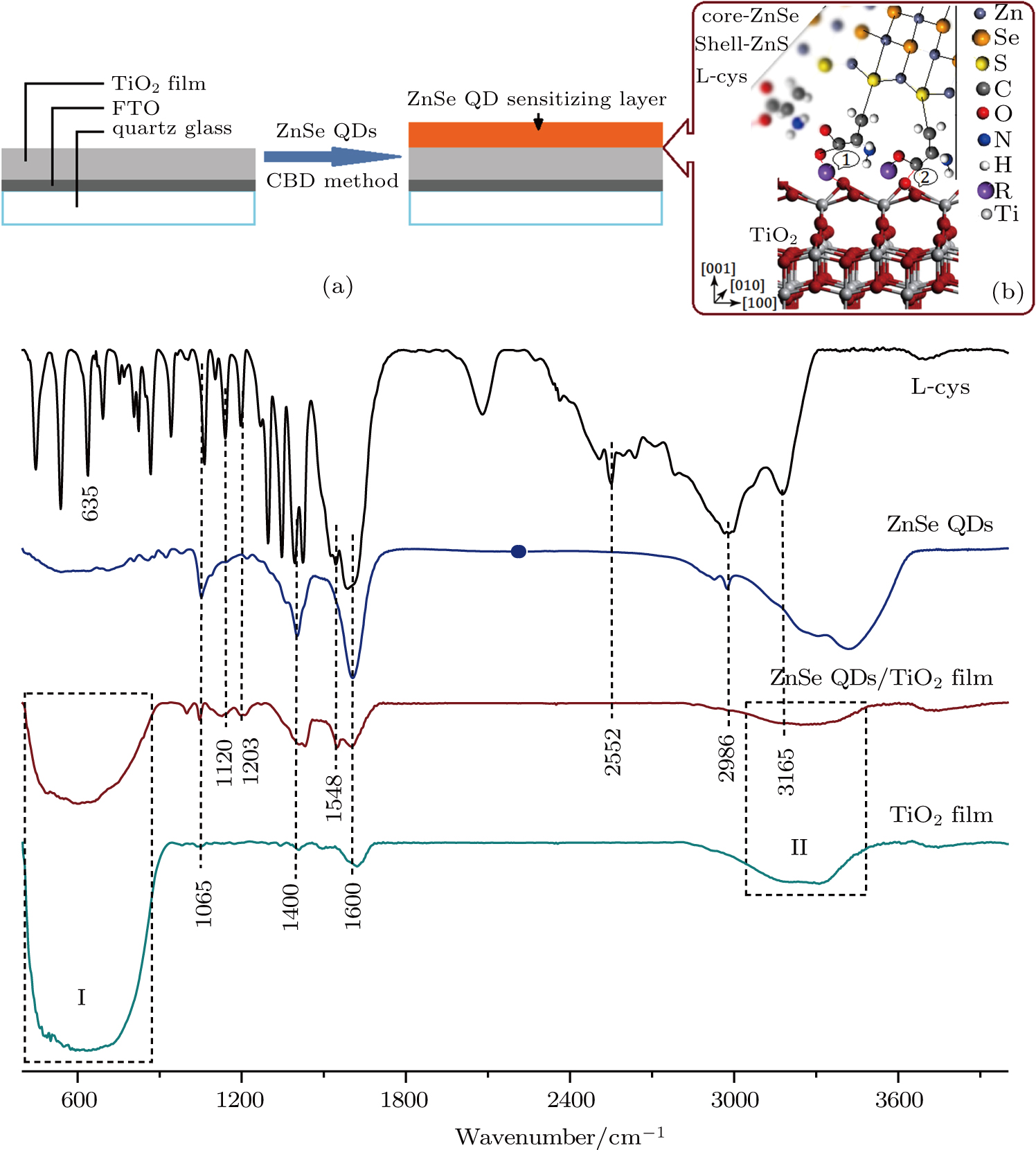
Fig. 1. (color online) FT-IR absorption spectra of pure L-Cys, self-assembled core–shell ZnSe/ZnS/L-Cys QDs, mesoporous La-doped nano-TiO2 thin film, and ZnSe QD-sensitized nano-TiO2 thin film. Inset (a) shows the cross-section of TiO2 thin film before and after sensitizing. Inset (b) illustrates a possible pattern of molecular linking at the phase interface of the core–shell ZnSe/ZnS/L-Cys QDs and TiO2 thin film.[27]

However, those peaks marked by red numbers either disappear or weaken in the IR adsorption spectrum of the QD-sensitized thin film. In particular, the stretching vibration band of the S–H bond disappears at 2557 cm−1, whereas the stretching vibration band of the C–S bond at 635 cm−1 weakens and shifts to a higher frequency. The former suggests that the S–H bonds in the L-Cys ligand are broken during the formation of the QDs; the latter is caused by the formation of Zn–S bonds between the ZnSe core and L-Cys as seen in Fig. 1(b). Moreover, the symmetric and asymmetric stretching vibrations of the –CH2 groups at 3156 cm−1 and 2986 cm−1, respectively, for L-Cys do not appear in the IR spectrum of the QD-sensitized thin film. This implies that a new chemical bond may be formed between the core–shell ZnSe/ZnS/L-Cys QDs and the TiO2 thin film substrate as described in the case 1 in Fig. 1(b). The stretching vibration bands of the carboxyl groups at 1600 cm−1 and 1548 cm−1 for L-Cys weaken or disappear in the IR spectrum of the QD-sensitized thin film. This indicates that other chemical bonds probably form between the oxygen atoms of the –COOR groups and unsaturated Ti atoms at surface of the TiO2 thin film as illustrated in the case 2 in Fig. 1(b). In addition, both the twisting vibration band of the Ti–O–Ti bond and the stretching vibration band of the Ti–O bond appear in region I in Fig. 1. In addition, the absorption band that appears in region II in Fig. 1 may be attributed to the interaction between the unsaturated Ti atoms and H2O molecules adsorbed on the surface.[27] Consequently, both the QDs and the substrate nano-TiO2 are not a simple stacking. The L-Cys ligand not only acts as a stabilizer of the core–shell QDs but also plays a role in molecularly linking the ZnSe QDs with nano-TiO2 thin film to form an effective nanocomposite film.

3.2. UV-VIS adsorption spectrum analysis

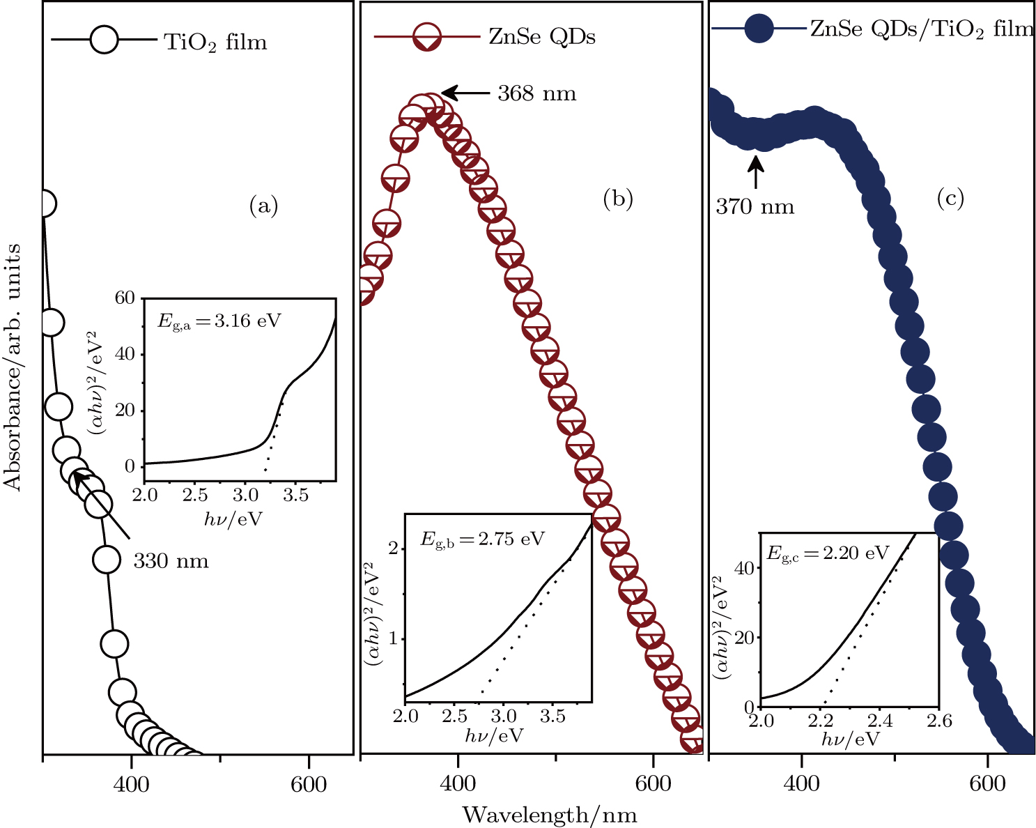
Room-temperature UV-VIS adsorption spectra of the as-prepared nano-TiO2 thin film, ZnSe QDs, and ZnSe QD-sensitized nano-TiO2 thin film are shown in Figs. 2(a)2(c), respectively. The exciton absorption peaks of the three samples appear respectively at 330 nm, 368 nm, and 370 nm as arrowed in Figs. 2(a)2(c).

Fig. 2. (color online) Room-temperature UV-VIS absorption spectra of (a) as-prepared nano-TiO2 thin film with three layers, (b) ZnSe QDs, and (c) ZnSe QD-sensitized nano-TiO2 thin film at the sensitized temperature of 60 °C for 5.0 h. The corresponding Tauc relations are illustrated as plots in insets.

The values of optical bandgap, Eg, of these samples are estimated using the Tauc relation shown in the insets of Fig. 2,[28,29] i.e., Eg values of the nano-TiO2 thin film, the ZnSe QDs, and the ZnSe QD-sensitized nano-TiO2 thin film are 3.16 eV, 2.75 eV, and 2.20 eV, respectively. A strong quantum confinement effect may occur in the ZnSe QDs because their crystallite size (2.25 nm), which is estimated by the Scherrer formula, is far smaller than the Bohr radius of bulk ZnSe (4.5 nm).[20,30] The dependence of QD size on both pH value and reaction temperature is displayed in Fig. S4 in Appendix A. Thus, the bandgap of the ZnSe QDs should be larger than that of bulk ZnSe (2.69 eV). Obviously, the absorption range of the QD-sensitized nano-TiO2 thin film is broadened to include the range from UV light to visible light compared with that of the nano-TiO2 thin film. Meanwhile, the absorption intensity of the former is much stronger than that of the latter as shown in Fig. 2. According to Ref. [31], the quantum confinement energy, ΔEg, can be obtained from the following equation: where m* is the reduced mass ( and ), m0 is the electron rest mass, h is the Planck constant, and D is the average diameter of the QDs determined by the Scherrer formula.[19] The ΔEg value of the ZnSe QDs is 0.529 eV.

3.3. TPV and SPV spectra analysis

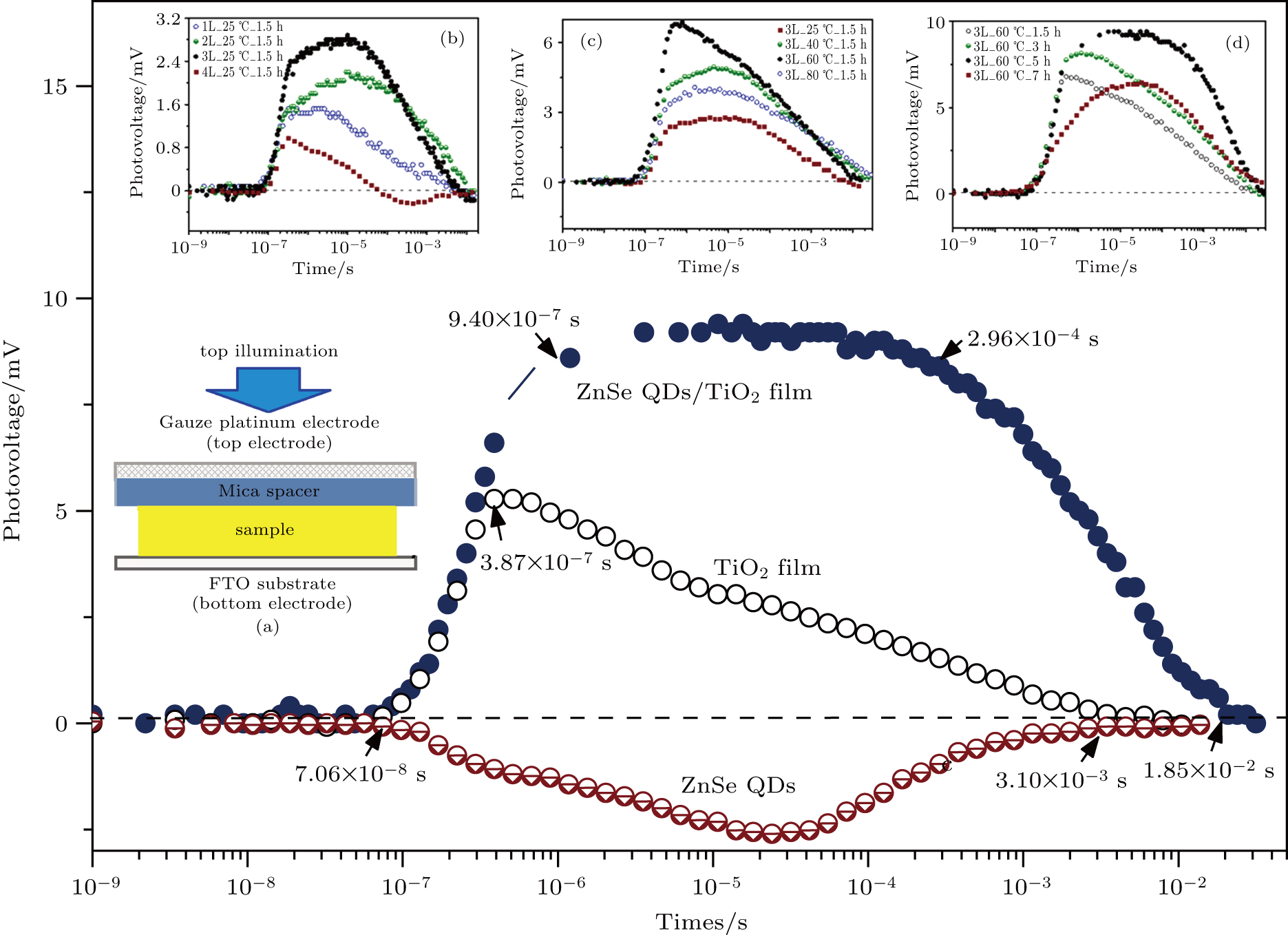
According to Ref. [22], SPV technologies can also be used effectively to obtain the information about photoelectron behaviors at surfaces and phase interfaces, because the techniques are by no means sensitive only to surfaces. Rather, they are sensitive to the entire surface SCRs by super- or sub-bandgap absorption, even to buried interfaces located anywhere in the sample, as long as they can be reached by photons. The TPV spectra of the nano-TiO2 thin film, the ZnSe QDs, and the QD-sensitized nano-TiO2 thin film are shown in Fig. 3. The home-build setup for the TPV spectroscopy measurements is illustrated in Fig. 3(a), where the sample is illuminated by a laser with a wavelength of 355 nm and an intensity of 20 μJ. According to Ref. [32], a semiconductor exhibits p-type TPV characteristics when the polarity of the TPV response of the semiconductor is negative. The p-type TPV characteristics result from the movement of negative charges, which arise from electron-hole pairs created by the illumination of the laser pulse, from the bulk to the surface of the semiconductor on the illuminated side. Conversely, a semiconductor possesses n-type TPV characteristics when the polarity of the TPV response of the semiconductor is positive. Three variables in the preparation process of the nanocomposite film, i.e., the layer of TiO2 thin film substrate, the sensitized temperature, and the sensitized time, are the major factors affecting the time-resolved photovoltaic characteristics of the nanocomposite film as seen in Figs. 3(b)3(d). Of them, however, the sensitized time is the most important one because it shows more notable influences on both the intensity and the range of the PTV response than the other two. A similar result is confirmed by the UV-VIS absorption spectra of these samples as shown in Fig. S5 (see Appendix A). The scanning electron microscopy images of the QD-sensitized nano-TiO2 thin film obtained at different sensitized times are shown in Fig. S6. Here, we focus on discussing the TPV and SPV characteristics of the as-prepared QD-sensitized thin film, which has a three-layer nano-TiO2 coating and is sensitized at 60 °C for 5.0 h, according to the test results above. In addition, the time period of the PTV response for each sample in Fig. 3 can be divided into three regions. Specifically, the absolute value of the intensity of the TPV response increases with time going by in range 1; the peak intensity of the PTV response is generally unchanged over time in range 2; and the absolute value of the intensity of the TPV response decreases with time increasing in range 3. In a normal case, the separation rate of photogenerated electron-hole pairs is faster than their recombination rate before reaching the peak intensity of the TPV response. In contrast, the recombination rate is faster than the separation rate after reaching the peak according to Ref. [32].

Fig. 3. (color online) TPV spectra of the as-prepared nano-TiO2 thin film with three layers, ZnSe QDs, and ZnSe QD-sensitized nano-TiO2 thin film obtained at the sensitized temperature of 60 °C for 5.0 h. Inset (a) illustrates the home-build setup for TPV spectrum measurement, where the sample is illuminated by a laser with a wavelength of 355 nm and an intensity of 20 μJ. Inset (b) shows the TPV spectra of the ZnSe QD-sensitized nano-TiO2 thin film with various layers of the substrate thin film. Inset (c) shows the TPV spectra of the ZnSe QD-sensitized nano-TiO2 thin film obtained at different sensitized temperatures. Inset (d) is the TPV spectra of the ZnSe QD-sensitized nano-TiO2 thin film obtained at different sensitized times. Capital L in each of insets (b)–(d) represents the number of nano-TiO2 coating layers.

First, it is interesting that the QD-sensitized nano-TiO2 photoanode shows n-type TPV characteristics, unlike the ZnSe QDs but similar to the TiO2 thin film, based on the results in Fig. 3. This phenomenon implies that the transport directions of photogenerated FCCs in the QDs are opposite before and after sensitizing, resulting in increased free electron transfer from the QDs to the thin film substrate via a new effective channel that is formed between them. This may be a primary cause of the higher intensity of the TPV response of the QD-sensitized nano-TiO2 thin film than those of the QDs and the nano-TiO2 thin film as shown in Fig. 3. In other words, the level of photogenerated FCCs with negative charge injection into the photoanode is greatly improved by the sensitization of the QDs. Second, the start time of the arising TPV response of the three samples occurs at 7.06 × 10⁻⁸ s in Fig. 3. However, the end time of region 1 of the QD-sensitized nano-TiO2 thin film is extended from 3.87 × 10⁻⁷ s to 9.40 × 10⁻⁷ s for the TiO2 thin film. Third, the PTV response of the QD-sensitized thin film disappears at 1.85 × 10⁻² s in region 3, which is extended by approximately an order of magnitude more than those of the nano-TiO2 thin film and the QDs as shown in Fig. 3. This result can be ascribed to the prolonged lifetime of photogenerated FCCs in the QD-sensitized thin film. Especially, the peak intensities of the TPV responses of the QD-sensitized thin films last a long time from 9.40 × 10⁻⁷ s to 2.96 × 10⁻⁴ s. However, the intensities of the TPV responses of both the nano-TiO2 thin film and the QDs immediately decrease over time after reaching their respective peaks in Fig. 3. These excellent time-resolved PV characteristics of the QD-sensitized thin film may be attributed to both a prolonged diffusion length of photogenerated FCCs and reduced recombination rate of photogenerated electron-hole pairs in the QD-sensitized thin film.

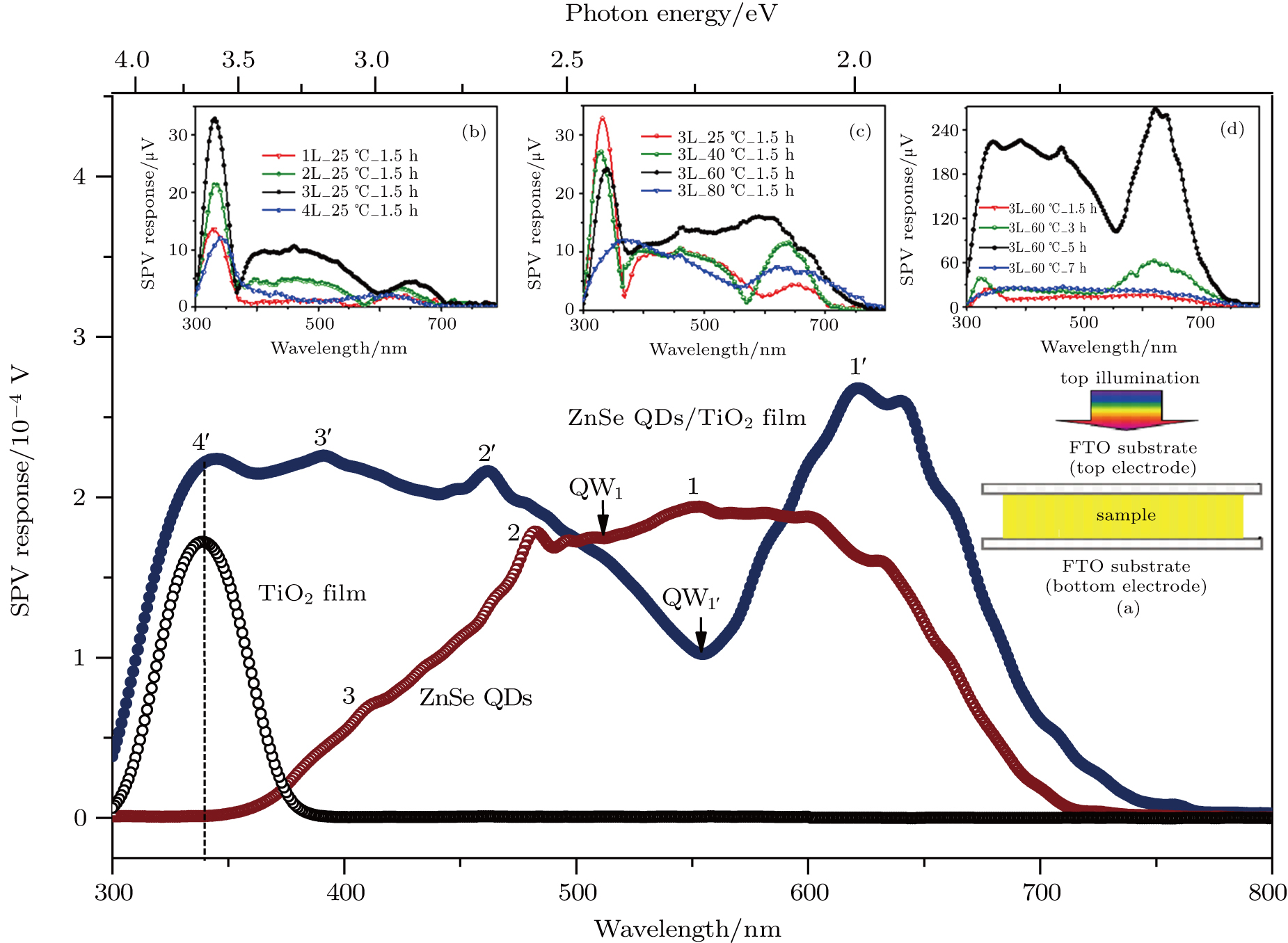
To further confirm the results above, figure 4 shows the SPV spectra of the nano-TiO2 thin film, the ZnSe QDs, and the QD-sensitized nano-TiO2 thin film. The home-built setup of SPV detection is illustrated in Fig. 4(a). Like the results in Figs. 3(b)3(d), the sensitized time is a key factor affecting the SPV characteristics of the QD-sensitized nano-TiO2 thin film as shown in Figs. 4(b)4(d). In addition, the QD-sensitized film displays the highest intensity and the widest range of the SPV response in the three samples. Importantly, some unique SPV characteristics of the QD-sensitized nano-TiO2 thin film are shown in Fig. 4. The SPV response of the nano-TiO2 thin film appears in a range of 300 nm–387 nm. The corresponding photoelectric threshold, Eg, TiO2 thin film, SPV, is 3.20 eV, which is in good agreement with the optical bandgap, Ega (3.16 eV). The photoelectric threshold of the SPV response can be determined by the abscissa for the largest external tangent of the band. According to our previous research,[21] knees 1, 2, and 3, which are marked in the SPV spectrum of the self-assembled core–shell ZnSe QDs in Fig. 4, are related to the band-band transitions of the ZnSe core, ZnS shell, and outer layer L-Cys ligand, respectively. Their photoelectric thresholds are Eg, ZnSe core, SPV (1.85 eV), Eg, ZnS shell, SPV (2.10 eV), and Eg, outer–layer–L–Cys SPV (2.73 eV, which is consistent with Eg, b), respectively. The quantum confinement effect of the ZnSe QDs is confirmed by those results in Figs. S4 and S7 in Appendix A. That is, the photoelectric threshold of the core-ZnSe, Eg, ZnSe core, SPV, closely related to its optical bandgap, changes with the grain size of the QDs. The abbreviation QWi in Fig. 4 represents a quantum well that is buried in a certain interface space charge region. A formula was previously proposed by us,[21] i.e., the depth of QWi, to calculate ΔEWi, which is determined by the difference between the photon energy (EQWi) corresponding to QWi and the photoelectric threshold (Egi,SPV) of the peak closest to QWi on the long wavelength side of the SPV spectrum: Therefore, the estimated value of ΔEW1, where = EQW1Eg, core−ZnSe, SPV, is 0.53 eV, which is in good agreement with the quantum confinement energy, ΔEg. The SPV spectrum of the QD-sensitized nano-TiO2 thin film shows a great change in entire profile compared with those of the nano-TiO2 thin film and the QDs. Particularly, QW1′ of the QD-sensitized film and knee 1 of the QDs both appear at a wavelength of 552 nm (2.25 eV) in Fig. 4. The photoelectric threshold, Eg, 1′, SPV, of knee 1′ is 1.58 eV. The estimated value of ΔEW1′ is 0.67 eV according to Eq. (2).

Fig. 4. (color online) SPV spectra of the as-prepared nano-TiO2 thin film with three layers, ZnSe QDs, and ZnSe QD-sensitized nano-TiO2 thin film obtained at the sensitized temperature of 60 °C for 5.0 h. Inset (a) shows a schematic diagram of the home-built setup for stationary SPV spectrum measurements, in which light is generated using a 500-W Xenon lamp and regulated to 23 Hz with a light chopper. Inset (b) displays the SPV spectra of the ZnSe QD-sensitized nano-TiO2 thin film with various substrate thin film layers. Inset (c) presents the SPV spectra of the ZnSe QD-sensitized nano-TiO2 thin film obtained at different sensitized temperatures. Inset (d) exhibits the SPV spectra of the ZnSe QD-sensitized nano-TiO2 thin film obtained at different sensitized times. Capital L in each of insets (b)–(d) refers to the number of nano-TiO2 coating layers.

This implies that the depth of QW1′ is 0.14 eV deeper than that of QW1; a deeper QW will result in a higher quantum confinement energy. We suggest that knee 1′ in Fig. 4 depends strongly on sub-bandgap transition that is related to some interface states in the QD-sensitized thin film, as Eg, 1′, SPV (1.58 eV) is smaller than Eg, core-ZnSe, SPV (1.85 eV). The strong SPV response of knee 1′ indicates that these interface states, such as cases 1 and 2 illustrated in Fig. 1(b), not only trap many photogenerated carriers with negative charges from the QD sensitizer but also greatly improve the level of electrons injected into the photoanode. Similar inference can be obtained by the cases of knees 2′ and 3′ in Fig. 4. However, knee 4′ is exactly located at a wavelength of 339.7 nm, which corresponds to the peak intensity of the SPV response of the nano-TiO2 thin film, as seen in Fig. 4. Therefore, the sensitization of the QDs plays a very important role in the transport process of photogenerated FCCs of the nanocomposite film, because of a considerable difference in those SPV spectra among the composite film, the quantum dots, and the substrate nano-TiO2 in Fig 4.

Table 1.

Relevant parameters of samples.

.
4. Conclusions

In summary, the ZnSe QD-sensitized nano-TiO2 photoanode exhibits excellent time-resolved and steady-state photovoltaic characteristics. The results reveal that the L-Cys ligand acts as a molecular linker between the QD sensitizer and the nano-TiO2 thin film substrate mainly by the carboxy groups. A new FCC transport channel, which is formed at the phase interface, may be responsible for the transformation of the TPV characteristics from p-type for the QDs to n-type for the QD-sensitized thin film, and for the enhanced and widened photovoltaic responses of the nanocomposite thin film. The specific microstructures of the interface states between the QDs and the substrate result in prolonged lifetime and diffusion length of photogenerated FCCs. This greatly increases the level of electron injection into the photoanode. In addition, the results confirm that the formula, which was previously proposed by us and was used for evaluating the QW depth in the surface SCR of group II/IV core–shell QDs, also used to evaluate the QW depth in the interface SCR of the nanocomposite film consisting of core–shell ZnSe QDs and La-doped nano-TiO2.

Reference
[1] Gratzel M 2001 Nature 414 338
[2] Klimov V I 2006 J. Phys. Chem. 110 16827
[3] Ahmed R Zhao L Mozer A J Will G Bell J Wang H 2015 J. Phys. Chem. 119 2297
[4] Mora-Seró I Bisquert J 2010 J. Phys. Chem. Lett. 1 3046
[5] Cao Y Bai Y Yu Q Cheng Y Liu S Shi D Gao F Wang P 2009 J. Phys. Chem. 113 6290
[6] O’Regan B Gratzel M 1991 Nature 353 737
[7] Tubtimtae A Lee M W 2012 Thin Solid Films 526 225
[8] Kamat P V 2008 J. Phys. Chem. 112 18737
[9] Zhu Z Qiu J Yan K Yang S 2013 ACS Appl. Mater. Interfaces 5 4000
[10] Santra P K Nair P V Thomas K G Kamat P V 2013 J. Phys. Chem. Lett. 4 722
[11] Diguna L J Shen Q Kobayashi J Toyoda T 2007 Appl. Phys. Lett. 91 023116
[12] Dang T C Pham D L Le H C Pham V H 2010 Adv. Nat. Sci.: Nanosci. Nanotechnol. 1 015002
[13] Jostar T S Devadason S Suthagar J 2015 Mater. Sci. Semicond. Process. 34 65
[14] Sauvage F Fonzo F D Bassi A L Casari C S Russo V Divitini G Ducati C Bottani C E Comte P Graetzel M 2010 Nano Lett. 10 2562
[15] Dar M I Ramos F J Xue Z Liu B Ahmad S Shivashankar S A Nazeeruddin M K Grätzel M 2014 Chem. Mater. 26 4675
[16] Pareek A Paik P Borse P H 2014 Langmuir 30 15540
[17] Yang J Wang J Zhao K Izuishi T Li Y Shen Q Zhong X 2015 J. Phys. Chem. 119 28800
[18] Li K Y Wei S L Yang W Y 2011 J. Phys. Chem. Solids 72 643
[19] Li K Y Sun Z P Xue Z J 2012 Mater. Chem. Phys. 137 246
[20] Shan Q S Li K Y Xue Z J Lin Y Y Yin H Zhu R P 2016 J. Appl. Phys. 119 054301
[21] Li K Y Shan Q S Zhu R P Yin H Lin Y Y Wang L Q 2015 Nanoscale 7 7906
[22] Kronik L Shapira Y 1999 Surf. Sci. Rep. 37 1
[23] Chen Z Zhao G Li H Han G Song B 2009 J. Am. Ceram. Soc. 92 1024
[24] Legrand-Buscema C Malibert C Bach S 2002 Thin Solid Films 418 79
[25] Chang C H Lee Y L 2007 Appl. Phys. Lett. 91 053503
[26] Dhawale D More A Latthe S S Rajpure K Lokhande C 2008 Appl. Surf. Sci. 254 3269
[27] Wan Y Sun H Tan S Feng H Cheng Z Zhao J Zhao A Wang B Lu Y Yang J Hou J G 2013 Nat. Commun. 4 2214
[28] Tauc J Menth A 1972 J. Non-Cryst. Solids 8 569
[29] Winter J O Gomez N Gatzert S Schmidt C E Korgel B A 2005 Colloids Surf. 254 147
[30] Brus L E 1984 J. Chem. Phys. 80 4403
[31] Marple D 1964 J. Appl. Phys. 35 1879
[32] Mahrov B Boschloo G Hagfeldt A Dloczik L Dittrich T 2004 Appl. Phys. Lett. 84 5455