† Corresponding author. E-mail:
The mechanism for electrical conduction is investigated by the dark temperature-dependent current–voltage characteristics of Si PIN photodiodes with different photosensitive areas. The characteristic tunneling energy E00 can be obtained to be 1.40 meV, 1.53 meV, 1.74 meV, 1.87 meV, and 2.01 meV, respectively, for the photodiodes with L = 0.25 mm, 0.5 mm, 1 mm, 1.5 mm, and 2 mm by fitting the ideality factor n versus temperature curves according to the tunneling-enhanced recombination mechanism. The trap-assisted tunneling-enhanced recombination in the i-layer plays an important role in our device, which is consistent with the experimental result that area-dependent leakage current is dominant with the side length larger than 1 mm of the photosensitive area. Our results reveal that the quality of the bulk material plays an important role in the electrical conduction mechanism of the devices with the side length larger than 1 mm of the photosensitive area.
Silicon PIN photodiodes have wide applications in IR remote controls, industrial electronics, defense, security, medical and scientific instruments, etc. due to their high sensitivity and low cost.[1–3] The sensitivity of a photodetector determines the lowest light intensity that can be detected, which reflects the image definition.[4] The leakage current directly relates to the sensitivity of the detector, hence, it is important to understand the electrical conduction mechanism inside. It is generally believed that the leakage current is composed of bulk diffusion current, generation–recombination current of minority carriers in the space-charge region,[5,6] tunneling current at the p/i interface, etc.[7] Besides the material quality and electric-field design inside, the perimeter-to-area of the photosensitive region also influences the leakage current of the device.[8–10] In this paper, the quantitative analyses of the electrical properties of the Si PIN photodiodes with different photosensitive areas are demonstrated by the temperature-dependent current–voltage (I–V) measurement method. It is shown that the trap-assisted recombination plays a more important role in the dark carrier transport mechanism with the increase of the device size. The scalability study indicates that the perimeter of the photosensitive region affects the dark current more than their photosensitive area when the side length of the photosensitive region is below 0.5 mm.
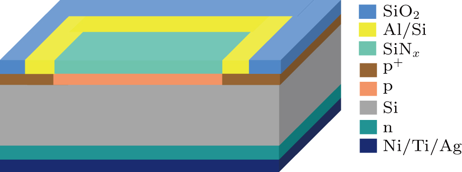
The cross-sectional diagram of the Si PIN photodetector studied in this paper is illustrated in Fig.
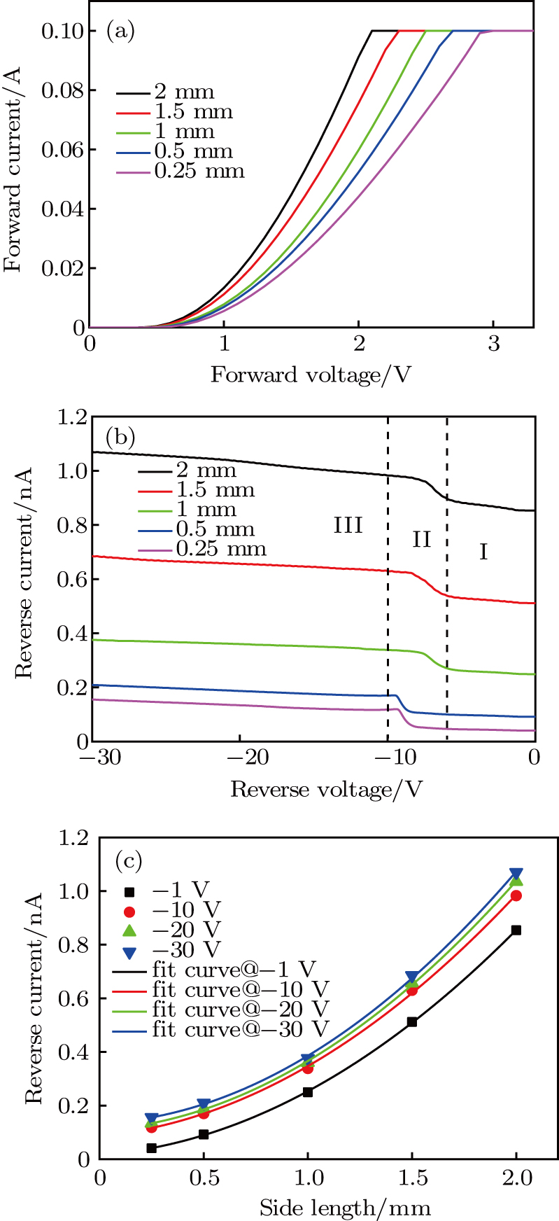
Figure
 |
The reverse dark current can be decomposed into the length-dependent part generated from the edge of p–n junction, the area-dependent part generated in or close to the depletion region, and a compensation current which depends on neither area nor circumference.[15] Thus, the total leakage current with the side length can be expressed as follows:
 |
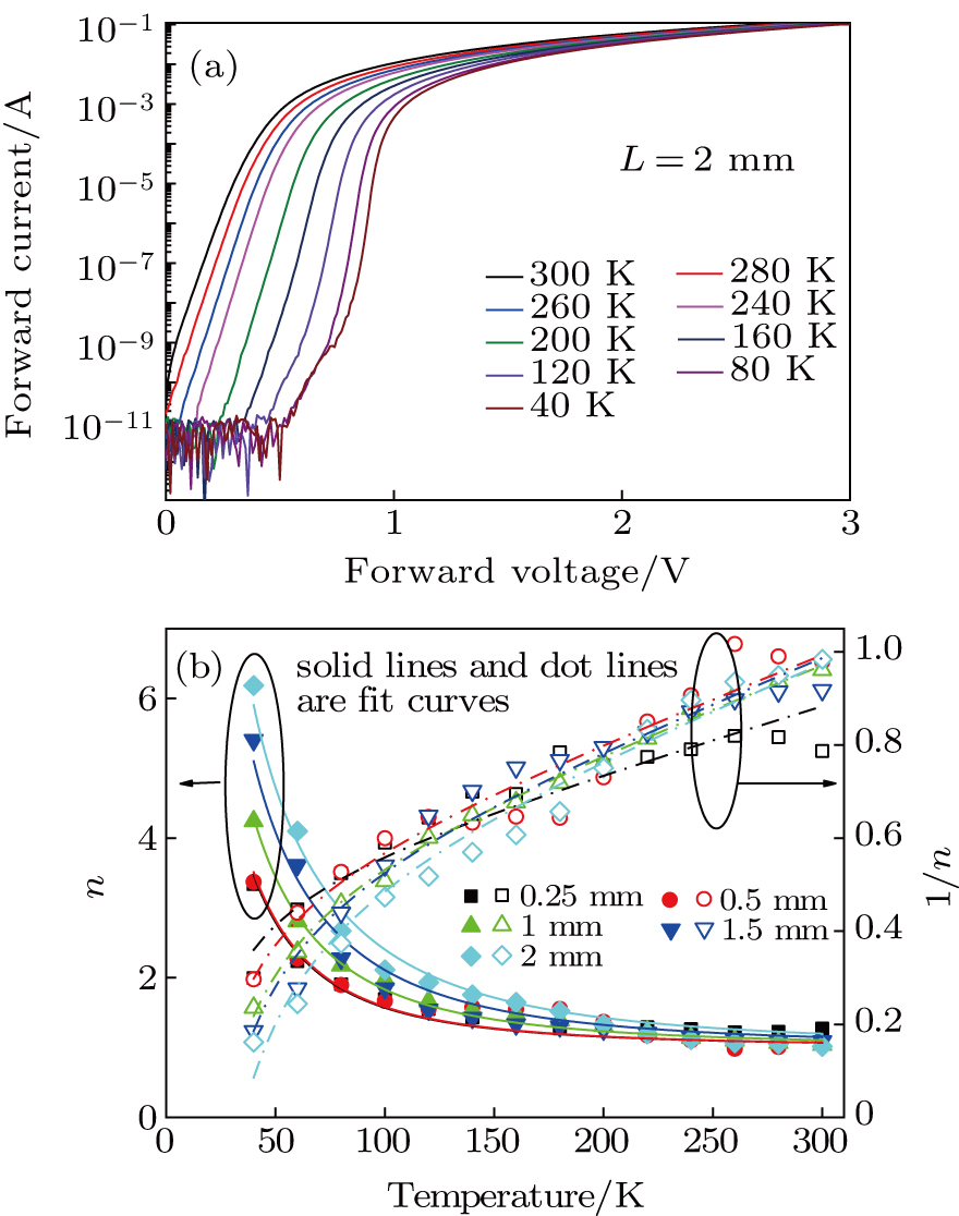
In order to further study the electric conduction behaviors in the Si photodiodes, the temperature-dependent I–V curves are measured. Figure
The tunneling-enhanced recombination assisted by defects or traps in the bulk material or close to the junction interface can be expressed, respectively, as[17–21]
 |
 |
Figure
In this paper, the scalibity of the electrical conduction mechanism has been investigated for the Si PIN photodiode. The forward temperature-dependent I–V measurement results demonstrate that trap-assistant recombination can be used to explain the electronic loss mechanism. The quality of the bulk material plays an important role in the electrical conduction mechanism for the devices with the side length larger than 1 mm of the photosensitive area.
| 1 | |
| 2 | |
| 3 | |
| 4 | |
| 5 | |
| 6 | |
| 7 | |
| 8 | |
| 9 | |
| 10 | |
| 11 | |
| 12 | |
| 13 | |
| 14 | |
| 15 | |
| 16 | |
| 17 | |
| 18 | |
| 19 | |
| 20 | |
| 21 |


