


Effects of growth conditions on optical quality and surface morphology of InGaAsBi
Cite this Article
Li Jia-Kai, Ai Li-Kun, Qi Ming, Xu An-Hui, Wang Shu-Min. Effects of growth conditions on optical quality and surface morphology of InGaAsBi. Chinese Physics B, 2018, 27(4): 048101 
Permissions
Effects of growth conditions on optical quality and surface morphology of InGaAsBi
† Corresponding author. E-mail:
Abstract
The effects of Bi flux and pressure of AsH3 on Bi incorporation, surface morphology and optical properties of InGaAsBi grown by gas source molecular beam epitaxy are studied. It is found that using relatively low pressure of AsH3 and high Bi flux can strengthen the effect on the incorporation of Bi and increase its content linearly with Bi flux until it nearly reaches a saturation value. The result from Rutherford backscattering spectroscopy (RBS) confirms that the Bi incorporation can increase up to 1.13%. By adjusting Bi and As flux, we could improve the surface morphology of InGaAsBi sample. Room temperature photoluminescence shows strong and broad light emission at energy levels much smaller than the InGaAs bandgap.
1. Introduction
The host III–V compound material which a small quantity of bismuth (Bi) atoms is incorporated into has attracted much attention due to its unique properties of the strong enhancement of spin-orbit splitting and large band-gap reduction.[1–5] Bismuth is the largest and heaviest group V element with its isoelectronic energy level that resides in the valence bands of most III–V materials,[6] therefore, substituting As and/or P with a small amount of Bi into InP, GaAs, or InGaAs will result in anomalously narrow bandgaps[7,8] due to valence band anticrossing (VBAC).[9–12] Engineering the band structure for potential optoelectronic and electronic device applications is possible because of these interesting properties.[13–16] Also, InGaAs alloy, which is widely used as a fundamental material in photonic devices, is expected to be turned into a promising temperature-insensitive semiconductor InxGa1−xAs1−yBiy by Bi incorporation.
In 2005, the first InGaAsBi quaternary alloy was grown on InGaAs buffer layer on an InP substrate by Gan et al. using molecular beam epitaxy (MBE).[12] Good crystalline quality was achieved with 2.5% Bi, which was confirmed by x-ray diffraction (XRD). Two years later, the same research group investigated temperature dependence of Bi behavior during MBE growth.[11] They achieved a maximum of 6% Bi concentration at a growth temperature as low as 260 °C. The growth at a high temperature of 450 °C, normally for InGaAs epitaxy growth, revealed no detectable Bi incorporation but the decrease of surface roughness from 1.067 nm to 0.328 nm.[17] In 2017, Zhou et al. demonstrated that up to 7.5% of Bi incorporation was achieved in InGaAsBi,[18] which was the highest Bi content until now. For the applications of InGaAsBi in electronic and optoelectronic devices, a short-wave infrared detector with quaternary InGaAsBi as an absorption layer and the bismuth content of about 3.2% has red-shifted the 50% cut-off wavelength from about 

In this work we systematically study the effects of growth condition, including Bi flux and pressure of AsH3 on Bi incorporation, surface morphology and optical properties of InGaAsBi grown by the gas source molecular beam epitaxy(GSMBE) method.
2. Experimental methods
All InGaAsBi samples were grown on (100) semi-insulating InP substrates by a V90 GSMBE system. Elements In, Ga, Bi, and As2 coming from arsine (AsH3) at 1000 °C were used as source materials. Elements In, Ga, and Bi fluxes during growth were controlled by adjusting the respective effusion cell temperatures. Prior to growth, by slowly ramping up the manipulator temperature, the substrate surface was deoxidized under P2 pressure until the reflection high-energy electron diffraction (RHEED) pattern showed a clear and abrupt transformation to a (2 × 4) surface reconstruction. This surface reconstruction was adopted as a means for calibrating the substrate temperature. After that, InGaAsBi epilayers with a thickness of about 
| Table 1.
Material growth parameters and measured properties of the grown InGaAsBi at different Bi effusion cell temperatures. . |
| Table 2.
Material growth parameters and measured properties of grown InGaAsBi at different pressures of AsH3. . |
After growth, the Bi compositions were determined by Rutherford backscattering spectroscopy (RBS) with 2.275-MeV 4He2+ ions. The structures of all samples were characterized by ω–2θ scans along the (004) direction, performed in a Philips X’pert high resolution x-ray diffractometer (HRXRD) equipped with a Ge (220) four-bounce monochromator using Cu–Kα1 (λ =0.15406 nm) radiation. Their surface morphologies and roughness values were measured by atomic force microscopy (AFM). Photoluminescence (PL) and absorption measurements were conducted in a Fourier transform infrared (FTIR) spectroscopy by using a liquid nitrogen-cooled InSb detector and a CaF2 beam splitter. A diode-pumped solid-state (DPSS) laser (λ =532 nm) was used as an excitation source for PL measurement.
3. Results and discussion
The RBS is a powerful method of determining the concentration of heavy atoms in a crystal lattice composed of light elements. A typical result of sample a2 is shown in Fig.
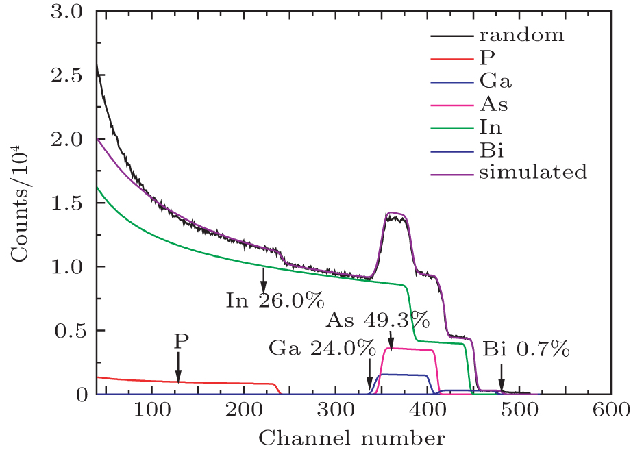 | Fig. 1. (color online) RBS spectrum from the InGaAsBi film with a Bi concentration of 0.7%. The black, violet, red, blue, magenta, olive, and navy lines represent the randomly and simulated spectra of the InGaAsBi films with the individual P, Ga, As, In, and Bi, respectively. |
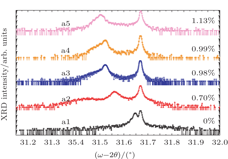
 | Fig. 2. (color online) HRXRD (004) ω–2θ scans for InGaAsBi epilayers on InP with Bi content of 0% (a1), 0.7% (a2), 0.98% (a3), 0.99% (a4), and 1.13% (a5). |
Lattice constants are assumed to be 6.639, 6.234, 6.058, and 5.653 Å for InBi, GaBi, InAs, and GaAs in zinc blende structures, respectively.[22] Therefore, the amounts of Bi in the InGaAsBi alloys estimated from the lattice constant are around 0%, 0.70%, 0.98%, 0.99%, and 1.13%. The Ga has an effect to reduce the lattice constant after being incorporated into InP and InAs lattice.[23] It is expected that the lattice constant of InGaAsBi can be matched to that of InP by appropriately controlling the Ga and Bi content.
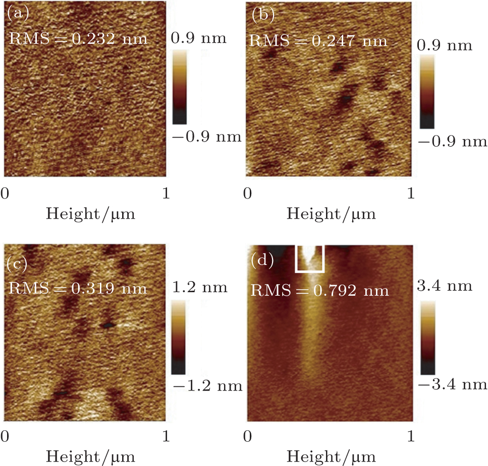
The surface morphologies are characterized by 
 | Fig. 3. (color online) Surface morphologies of the InGaAsBi samples a2 (a), a3 (b), a4 (c), and a5 (d). |
Figure
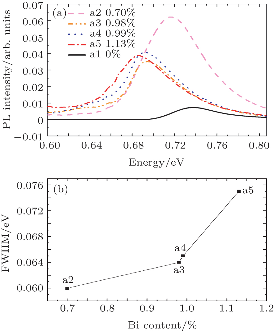 | Fig. 4. (color online) Room-temperature PL spectra for the samples with different Bi content. (b) Variations of the FWHM of the PL spectra of samples a2–a5 with their Bi content. |
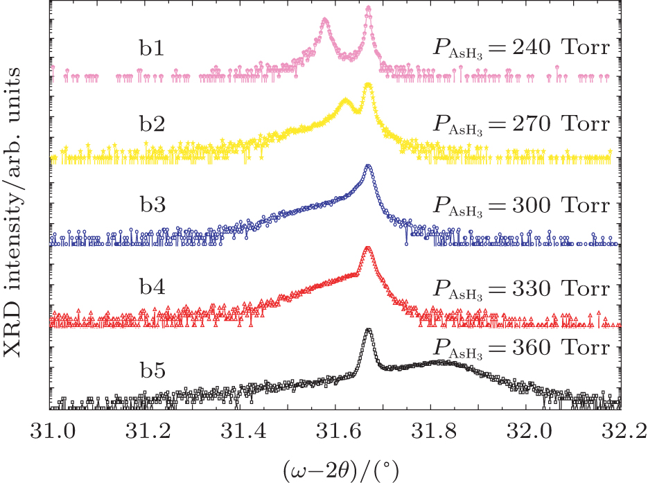
The InGaAsBi samples, with pressures of AsH3 varied but other conditions fixed, are renamed as b1, b2, b3, b4, and b5 as shown in Table
 | Fig. 5. (color online) HRXRD (004) ω–2θ scans for InGaAsBi epilayers (b1–b5) on InP at different AsH3 pressures. |
Figure
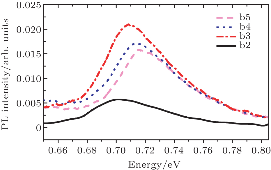
 | Fig. 6. (color online) Room temperature PL spectra for the samples b2–b5 at different AsH3 pressures. |
The PL spectra at room temperature of b2–b5 samples at different AsH3 pressures are shown in Fig.
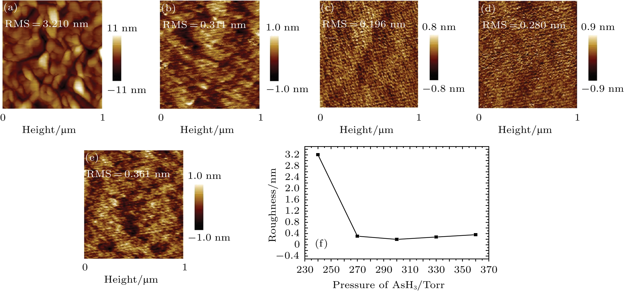
 | Fig. 7. (color online) (a)–(e) Surface morphologies of InGaAsBi samples b1, b2, b3, b4, b5. (f) Variations of the RMS roughness values of the InGaAsBi samples b1, b2, b3, b4, b5 with AsH3 pressure. |
4. Conclusions
In this work, we investigate the effects of Bi flux and AsH3 pressure during growth on Bi incorporation, surface morphology and optical properties of InGaAsBi grown by GSMBE on InP substrate. It is found that using high Bi flux and low AsH3 pressure during growth can strengthen the effect on the incorporation of Bi. The Bi content increases linearly with Bi flux until it reaches nearly a saturation value. The maximum incorporated Bi content is found to be 1.13%. A relatively low Bi flux and a moderate AsH3 pressure during growth can improve the surface morphology. We obtain the photoluminescence spectra of InGaAsBi at room temperature, which show strong and broad light emission at near infrared wavelength. The low AsH3 pressure will remarkably damage the optical properties of InGaAsBi grown by gas source molecular beam epitaxy.
Reference
| [1] | |
| [2] | |
| [3] | |
| [4] | |
| [5] | |
| [6] | |
| [7] | |
| [8] | |
| [9] | |
| [10] | |
| [11] | |
| [12] | |
| [13] | |
| [14] | |
| [15] | |
| [16] | |
| [17] | |
| [18] | |
| [19] | |
| [20] | |
| [21] | |
| [22] | |
| [23] | |
| [24] | |
| [25] |