1. IntroductionResistive random access memory (RRAM) is one of the most promising candidates for emerging nonvolatile memory, which is based on resistive switching (RS) between a high resistance state (HRS) and a low resistance state (LRS) under external electric stimulus.[1–3] The RS behavior has been intensively investigated in a large variety of oxide materials, including binary and perovskite-type oxides.[2–5] For unipolar RS, i.e., where the switching can be induced by an applied bias with the same polarity, the RS originates from the formation and rupture of nanometer-scale conducting filaments in the oxide layer.[6,7] From a microscopic point of view, the conductance filaments (CFs) are formed or ruptured in the nanoionic transport and redox reaction processes triggered by an electric field or temperature or both.[8] In oxides-based RS devices, the oxygen vacancy (ion) migration under an external electric field is an essential factor affecting the formation and rupture of CFs.[7–10] The reported work showed that unipolar RS has several merits, such as high-density, large off/on resistance ratio (103–106), and simpler design for drive circuits. However, there are still several key concerns including the inappropriate repeatability of the RS parameter and insufficient endurance, which are obstacles to realize the RRAM as a practical technology.[10–13] The commonly accepted opinion about the non-uniform RS performances with increasing the number of RS cycles is related to the non-uniform and uncontrolled formation and rupture of CFs over a large area of the memory cell, which is caused by their random nucleation and uncontrolled growth. Hence, we believe that it would be advantageous to define the location of the filamentary RS and growing direction of CFs to improve the performances of filamentary RS.
Previously, we reported that the unipolar RS behaviors independent of bias polarity were observed in Au/SrTiO3/Pt memory cells with 10-mA compliance current (CC).[14] Because it is difficult to achieve spatial information within a single layer RS material, we introduce NiO thin films between Au and SrTiO3 (STO) films in this work. The Au/NiO/STO/Pt cells exhibit unipolar RS, and the switching repeatability is closely related to the applied bias polarity. The spatial switching location and growing direction of CFs are further investigated based on the experimental results.
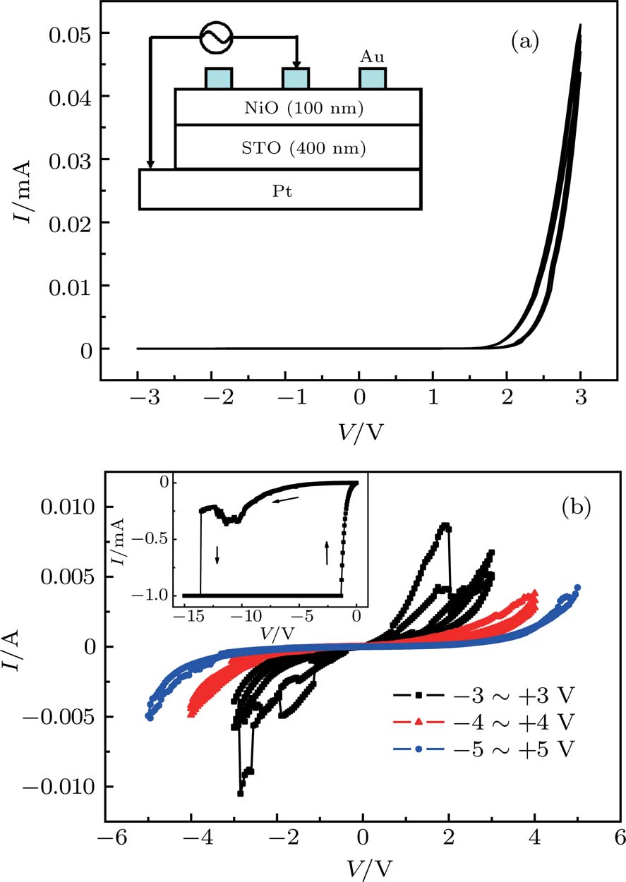
3. Results and discussionFigure 2(a) displays the I–V curves of the pristine Au/NiO/STO/Pt memory cell. The original resistance of this cell is large due to the presence of interface barriers, which can be identified by the rectifying I–V curves. It is well known that NiO is a p-semiconductor with Ni2+ vacancies formed by the nickel deficit, which provide holes for the valence band,[15] and STO is an n-semiconductor with oxygen vacancies which provide electrons for the conduction band.[16] So, p–n junctions are formed at the NiO/STO heterojunction interface, which brings about the unidirectional conduction characteristics under positive bias. Normally, an electroforming process is required to obtain conductance and activate reversible and reproducible RS behavior for a memory cell with high resistance. In the present work, the electroforming processes are completed in two steps. The first step is that a gradually increasing negative bias is applied until the current jumped to the compliance level of 1 mA as shown in the inset of Fig. 2(b). The current jump occurs at about 14 V for this cell. The second step is a voltage sweep with 10-mA CC under smaller bias range as shown in Fig. 2(b). Three repetitive I–V curves in a bias range of ±3 V show that the currents gradually decrease and become smooth with the bias scanning. The corresponding currents further decrease when the bias increases from ±3 V to ±5 V. After that, the rectification observed in the pristine state disappears and nearly symmetric I–V curves are seen. This indicates that the high density defect within the active thin film matrix is created under strong electrical stress, which is associated with the fact that oxygen-vacancy migration (or oxygen diffusion) is significantly enhanced along extended defects.
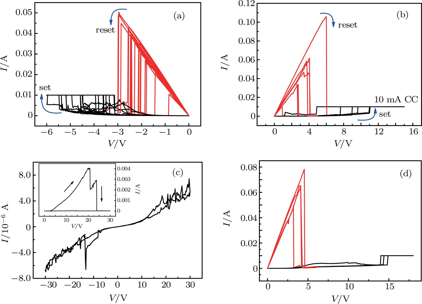
After electroforming, the Au/NiO/STO/Pt memory cells present unipolar RS behaviors, where the CC is controlled at 10 mA. Interestingly, the switching repeatability has strong dependence on the bias polarity. The cell shows reliable and repeatable unipolar RS under a negative bias as shown in Fig. 3(a). However, under a positive bias, this cell only displays a few switching cycles (about 4–7 cycles) and soon reaches the non-switching state irrespective of the CC (as shown in Fig. 3(b)). The inset in Fig. 3(c) exhibits the I–V curve of the last cycle, in which the cell remains in HRS and becomes higher at about 24 V. After this, the Au/NiO/STO/Pt cell cannot be recovered to the RS possible state even with 30 V bias as shown in Fig. 3(c). Moreover, the occurrence of the non-switching state is independent of the order of the positive or negative bias. If positive bias is applied to the cell after the electroforming process, the non-switching state is still observed after the RS has performed a few times (shown in Fig. 3(d)). This result is the same as that in Fig. 3(c). It should be noted that the Au/STO/Pt cells exhibit unipolar RS behaviors independent of bias polarity, which was shown in our previous work.[14] So, it can be deduced that such a bias polarity dependent unipolar RS behavior in Au/NiO/STO/Pt cells is closely related to the introduction of NiO film.
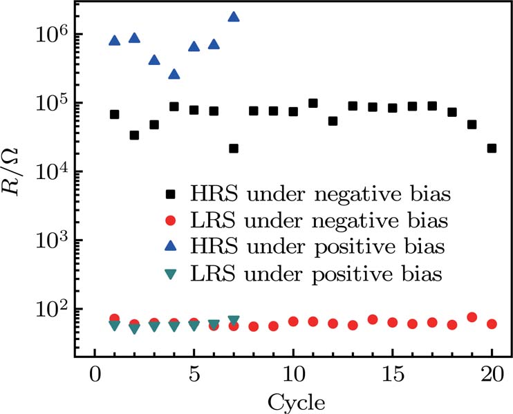
Figure 4 shows the resistance values of HRS and LRS under positive and negative bias, which are extracted from Figs. 3(a) and 3(b). There is no obvious difference in LRS, while the high resistance under positive bias is greater than that under negative bias. The high resistance values under negative and positive bias are within the ranges of
 and
and
 , respectively. Because the repeated unipolar RS originates from the formation and rupture of CFs, the current in HRS is distributed homogeneously across the cell area, and the current in LRS is localized to CFs.[7,17] So in this work, the different HRSs under positive and negative bias indicate that the bulk resistance of the NiO/STO stacked layer is affected by the bias polarity.
Comparing both types of reset switching curves in Figs. 3(a) and 3(b), the on-state I–V curves (i.e. curves in LRS) generally show Ohmic behaviors (i.e., linear I–V) in the low voltage region, indicating the metallic nature of CFs. However, the I–V curves each deviate from the linear shape in the high voltage region, which is due to the Joule heating effect that changes the Ohmic behaviors of CFs.[18] For a better understanding of the polarity-dependent unipolar RS in Au/NiO/STO/Pt cells, we investigate the relationship between the filament resistance and the Joule heating. Supposing that R0 is the filament resistance at room temperature, γ is the temperature coefficient of resistance, which is the intrinsic characteristic of an RS material, and
 is the temperature change in the filament, the filament resistance R, which will change due to the Joule heating effect, can be represented as follows:
 | |
The reset behavior originates due to the partial rupture of the metallic CFs by Joule heating. Lee et al. recently reported that
 in Eq. (1) is proportional to the power, specifically,
 (
(
 ),[19] where K is a coefficient. Therefore, equation (1) could be rewritten as
In Eq. (2), γ is the intrinsic characteristic of an RS material, and K is related to both the intrinsic property of a material such as heat capacitance of filament material, and the filament shape factor such as filament surface area for heat dissipation.
According to Eq. (2), the slope of the
 plot provides information about the
 value in each RS material system. For a given material system, γ is constant while K depends on R0 because the CF resistance is related to the shape and size of the CF.[18] The accurate quantitative relationship between K and R0 is difficult to determine at this point. However, the slope of the
 plot, which corresponds to the γK value, must be specific for each RS material system. Therefore, this type of plot can give a better indication of the material portion where RS actually occurs than the original switching I–V curves shown in Fig. 3.
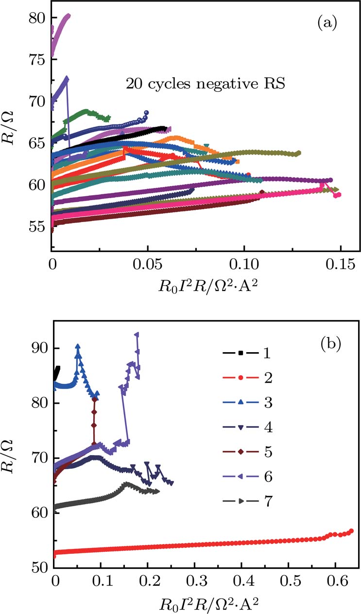
Figure 5 shows the
 plots of the on state I–V curves (V region up to the point immediately before reset occurs in Figs. 3(a) and 3(b)). In this type of plot, the graph generally has a linear shape in the low V region, suggesting constant material properties, but deviates from linearity before reset occurs due to the structural modification of the CF at this point. Therefore, an examination of the change in linear shape can provide clearer evidence where the reset switching occurs. The
 plot shows a regular shape only with a slight bend, and an abnormal shape with an abrupt increase and decrease under negative and positive bias, respectively as shown in Figs. 5(a) and 5(b). The slight deviation from the linear curve may be caused mainly by the changed filament resistance due to the Joule heating effect, but the abrupt increase and decrease should be induced not only by the Joule heating effect. We can deduce that the reset switching occurs in the same material under negative bias, but the CFs are ruptured within different material regions under positive bias.
Now it should be mentioned that the RS behavior of the Au/NiO/Pt cell has been studied. The experimental results show that the RS repeatability is closely related to the working pressure of O2 gas during the deposition of NiO film. We did not observe the repeated RS behaviors in the NiO film when the O2 pressure was 12 Pa which is used in this work. So it can be deduced that the repeated RS behaviors observed in the Au/NiO/STO/Pt cell are not caused by the NiO film. In addition, the repeated unipolar RS was observed in the Au/STO/Pt memory cells and was independent of bias polarity in our previous work.[14] According to these comparison results, we have a conclusion that the repeated RS behaviors in the Au/NiO/STO/Pt cell should be caused by the STO film. That is to say, the rupture and rejuvenation of CF occur in the STO film. The STO film is expected to comprise oxygen vacancies, which can be determined by the n-type material conduction characteristics according to the unidirectional conduction (as shown in Fig. 2(a)). So, in the set process, filamentary conducting paths, consisting of oxygen vacancies, are formed in STO films as a soft breakdown in the dielectric film and the device switches to LRS. There should be no filaments in the NiO layer because RS behavior is not observed in the Au/NiO/Pt cell. In the reset process, the filaments are disrupted by Joule heat generated by a high current (Ireset), so that the device returns to HRS.[14]
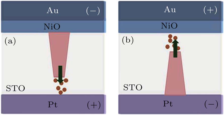
Figure 5 and the above analysis show that the switching should occur in different material regions, i.e., in STO film under negative and on the NiO and STO interface under positive bias. So, the unipolar RS depending on the bias polarity should be induced by the movement of the CF ruptured regions according to the bias direction. It is now widely accepted that the CFs in many oxide RS cells do not have a uniform cross-sectional area nor shape along their length direction.[20,21] Furthermore, the origin of RS behavior in STO is caused by oxygen vacancy or ion movement under an applied bias.[22,24–26] The negatively charged oxygen ions move toward the anode under applied bias, and simultaneously oxygen vacancies are created at the cathode and drift toward the anode, forming localized CFs in the oxide. This set process is accompanied with the thickening and thinning of the CFs in the vicinity of the cathode and anode interfaces, respectively. During the following reset process, more Joule heat is generated at the thin CF part by a high Ireset due to its large resistance, so the thin CF part is easily ruptured and actually responsible for the switching. Therefore, when a negative bias is applied to the Au/NiO/STO/Pt cell, the oxygen ions will transport from the Au to the Pt, resulting in the conduction paths comprised of oxygen vacancies as shown in Fig. 6(a). The rupture and rejuvenation regions of CFs occur at a weaker CF part near the STO/Pt interface, which results in repeated RS behaviors. When the positive bias is applied to the Au/NiO/STO/Pt cell, the oxygen vacancies generated at the STO/Pt interface would move toward the NiO/STO interface as shown in Fig. 6(b). The reset regions will move towards the weaker CF part. Ultimately, the reset region should be across the NiO/STO interface under positive bias — the corresponding reset curves as shown in Fig. 5(b) take on an abnormal shape with abrupt increase and decrease — which results in the non-switching state. In brief, the RS behaviors of the Au/NiO/STO/Pt cell occur near the anode, which is consistent with the reported results about n-type materials.[27–29] It might be reasonable to assume that an insulating oxide layer without oxygen vacancies is created at the NiO/STO interface. So a non-switching state is observed when positive bias is applied. This can also explain why the resistance of HRS in positive bias is greater than that in negative bias as shown in Fig. 4.


