Room-temperature operating extended short wavelength infrared photodetector based on interband transition of InAsSb/GaSb quantum well
Sun Ling1, 2, Wang Lu1, Lu Jin-Lei1, 2, Liu Jie1, 2, Fang Jun1, 2, Xie Li-Li3, Hao Zhi-Biao3, Jia Hai-Qiang1, Wang Wen-Xin1, Chen Hong1, †
Key Laboratory for Renewable Energy, Beijing Key Laboratory for New Energy Materials and Devices, Beijing National Laboratory for Condensed Matter Physics, Institute of Physics, Chinese Academy of Sciences, Beijing 100190, China
University of Chinese Academy of Sciences, Beijing 100049, China
Department of Electronic Engineering, Tsinghua University, Beijing 100084, China


† Corresponding author. E-mail: hchen@iphy.ac.cn

Abstract

Here in this paper, we report a room-temperature operating infrared photodetector based on the interband transition of an InAsSb/GaSb quantum well. The interband transition energy of 5-nm thick InAs0.91Sb0.09 embedded in the GaSb barrier is calculated to be 0.53 eV ( ), which makes the absorption range of InAsSb cover an entire range from short-wavelength infrared to long-wavelength infrared spectrum. The fabricated photodetector exhibits a narrow response range from to with a peak around at 300 K. The peak responsivity is 0.4 A/W under −500-mV applied bias voltage, corresponding to a peak quantum efficiency of 23.8% in the case without any anti-reflection coating. At 300 K, the photodetector exhibits a dark current density of 6.05×10⁻³ A/cm2 under −400-mV applied bias voltage and 3.25×10⁻⁵ A/cm2 under zero, separately. The peak detectivity is under zero bias voltage at 300 K.

1. Introduction

Research progress in infrared (IR) detector technology is mainly connected to the development of IR photodetectors, such as HgCdTe detectors, quantum well detectors, and superlattice detectors.[13] These detectors have been widely exploited in the fields of military surveillance, missile warning, guidance, etc.[4,5] The IR photodetectors exhibit a tunable and ultrafast response to the incident radiation with excellent signal-to-noise performance.[6] However, as the detection wavelength is longer, the narrower bandgap will result in increased thermal carriers, which significantly increase the dark current. In order to reduce the thermal noise, photodetectors require an exquisite cryogenic cooling system, which makes them bulky, expensive and have a short-life.[7,8]

Many efforts have been made to obtain photodetectors without the cryogenic cooling system operating in extended short-wavelength IR (eSWIR) and the mid wavelength IR (MWIR) ranges.[914] For example, p–i–n-type HgCdTe photodetectors operating at room temperature show high performances with suitable dopants,[13,15] while they require a complex material growth process and large area CdZnTe substrates are still unavailable.[16] Maimon and Wicks proposed a new type of barrier photodetectors,[17] such as InAsSb and HgCdTe nBn detectors,[1820] which can reduce dark current and noise without an impeding photocurrent to increase the operating temperature. In addition, cascade IR detectors, such as interband cascade devices based on type-II InAs/GaSb interband supperlattice absorbers,[21] have been introduced to avoid the limitation imposed by reduced diffusion length and effectively increase the absorption efficiency.[22] However, the performances of the last two types still need to be improved compared with those of the traditional HgCdTe photodetectors. Therefore, it is needed to develop novel IR photodetectors with low cost, high performance and being capable of operating at room temperature.

In general, the operating temperature of the IR photodetector is determined by dark current, which mainly consists of diffusion current and generation–recombination (GR) current. Both the dark currents are proportional to the square of the intrinsic carrier concentration of semiconductor material, while the intrinsic carrier concentration is determined by a natural bandgap. So the balance between absorption wavelength and dark currents dominates the device design and intrinsic limit of the detector performance.[23] Recently, it has been reported that the photo-excited carriers in a low-dimensional semiconductor material can be effectively extracted from a p–n junction.[2426] An InGaAs/GaAs quantum well (QW) prototype device based on such a phenomenon was already fabricated, which successfully proved the effectiveness of utilizing the interband transition of QWs as a new method of detecting IR spectra.[27] Because most of the device materials consist of wide bandgap barrier materials when using QWs, the dark current can be largely suppressed. Besides, based on the recently reported abnormal localized carrier extraction phenomenon, the absorption efficiency in thin QWs can be rather high, which can enhance the signal-to-noise ratio. So IR photodetectors based on the interband transition of QWs promise to achieve an effective high operating temperature in the IR detection.

As an ideal candidate material for fabricating the IR detectors, InAsSb can cover the wavelengths of MWIR and long-wave infrared (LWIR) with different antimony quantities.[28,29] Therefore, we here demonstrate a novel InAsSb/GaSb QW IR photodetector based on the interband transition. Such a detector has a working mechanism different from the currently widely used ones, which operate based on either inter sub-band transition of low-dimensional semiconductor materials, like GaAs/AlGaAs quantum well IR detectors, or interband transition of bulk material, like HgCdTe detectors. So it provides a new method to fabricate IR photodetectors operating at room temperature.

2. Calculation and experiment

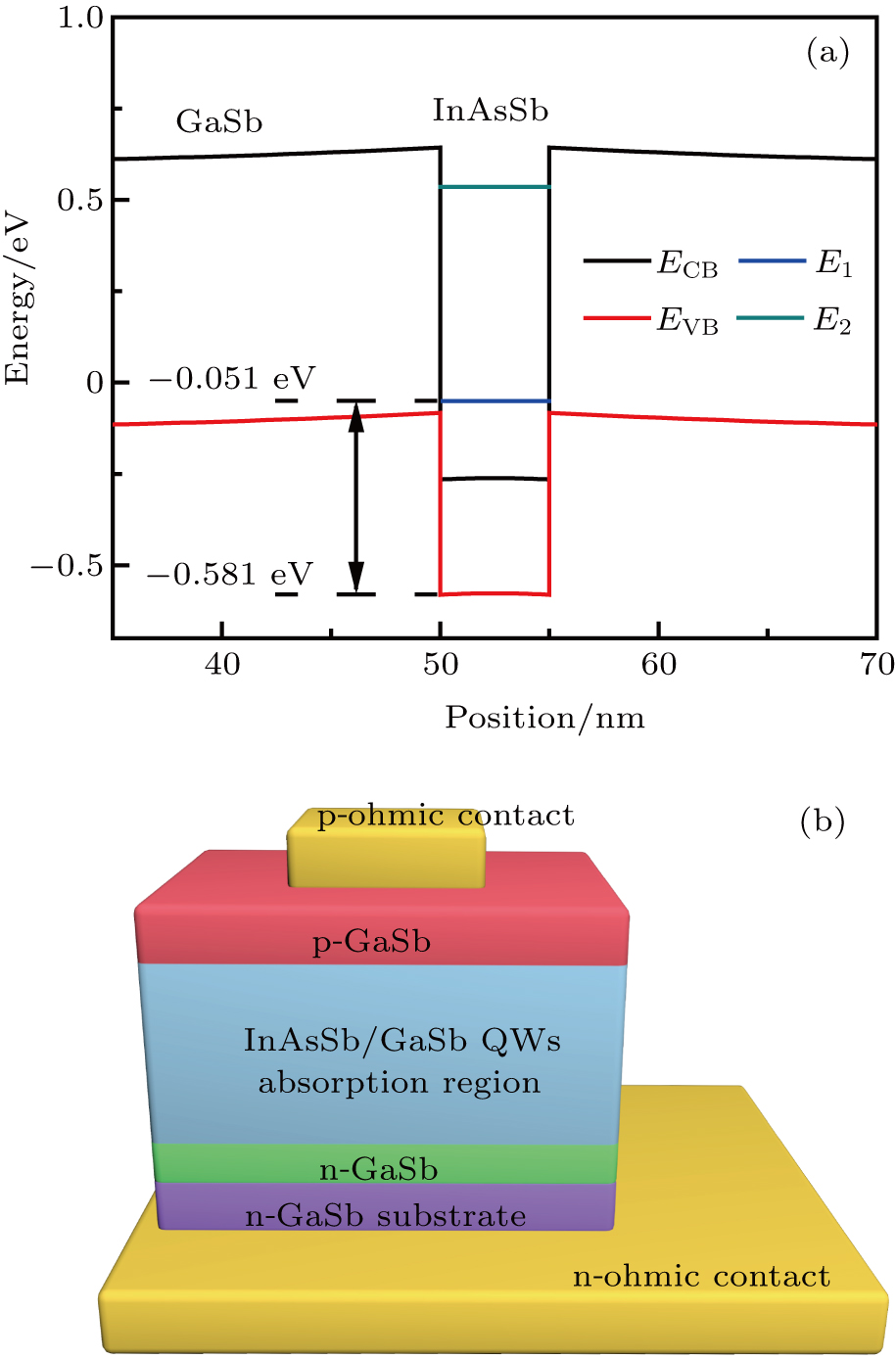
Since the energy level position is essential for designing an effective device, we first calculated the energy band structure of InAsSb/GaSb QW within the framework of effective-mass approximation as shown in Fig. 1(a). The strong quantum confinement in such a structure results in an obvious increase in E1 position compared with the conduction band (CB) of InAsSb. Nevertheless, E1 is still 35 meV higher than the valence band (VB) of GaSb, which makes the QW a type-II one. Since E1 is very close to the VB of GaSb, the type-II transition cannot be observed. The main transition that can be utilized in this structure is from VB of InAsSb ( to E1. The transition energy of 5-nm thick InAs0.91Sb0.09 (matched to the lattice constant of GaSb substrate) embedded in the GaSb barrier was calculated to be 0.53 eV ( ), much larger than 0.28 eV ( ) of bulk InAs0.91Sb0.09. So the absorption wavelength decreases from the MWIR range to the eSWIR range. Therefore, the small effective mass of the carrier of InAsSb makes the InAsSb/GaSb material system capable of covering the SWIR into LWIR spectrum range. The tunable absorption wavelength renders the InAsSb/GaSb QWs system an alternative for future wide response range and multi-color IR detectors.

Fig. 1. (color online) (a) Band structure of single 5-nm thick InAs0.91Sb0.09 QW embedded in GaSb bulk with a transition energy 0.53 eV ( ) from to E1. (b) Schematic diagram of the InAsSb/GaSb QWs photodetector.

Based on the principle of the interband transition of QWs and the calculation results, we designed the structure of the IR photodetector (Fig. 1(b)). The InAsSb/GaSb QWs were grown on an n-GaSb substrate in a V80H solid source molecular beam epitaxy reactor equipped with a valved arsenic cracker cell and a valved antimony cracker cell. The epitaxial growth started with growing a 400-nm-thick n-GaSb buffer layer to smooth the surface, then, a 100-nm un-doped GaSb barrier layer, followed by 10 periods of InAs0.91Sb0.09 (5 nm)/GaSb (50 nm) MQWs, a 200-nm-thick p-type GaSb (8×1017 cm−3), a 200-nm-thick p-GaSb (1×1018 cm−3) and 5-nm p-InAs (3×1018 cm−3). The Te and Be were used as the n-type dopant and p-type dopant, respectively. The growth temperature was 410 C, and the growth rates depending on gallium and indium beam flux were 5000 Å/h and 2000 Å/h, respectively.

After characterizing the crystal quality, the wafers were processed into a set of unpassivated mesa-isolated photodetectors with device area 1 mm2 by using the method of photolithography and wet etching. The electrodes of 20/100-nm Ti/Au were deposited onto the p-InAs in sequence by electron-beam evaporation. Then, 15/101/26/26/100-nm-thick Ni/Au/Ge/Ni/Au layers were deposited on the n-GaSb for an n-ohmic contact. The photodetectors were left unpassivated and had no anti-reflection coating. Then the sample was loaded into a cryostat with a germanium (Ge) window for both optical and electrical characterization. All the tests were carried out at room temperature except for the dark current.

3. Results and discussion

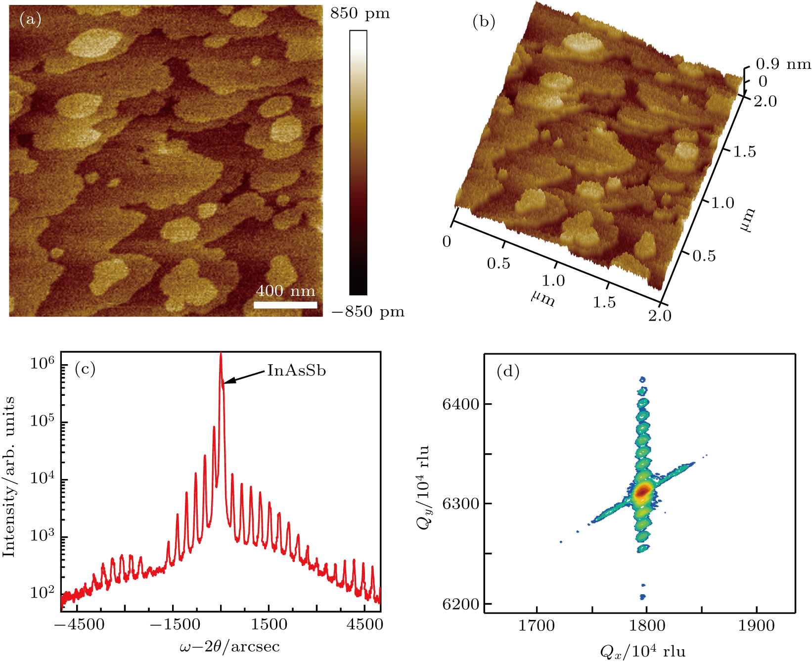
Crystal quality of epitaxial layer directly determines the performance of the subsequent device. Figures 2(a) and 2(b) exhibit the sample surface morphologies of the sample characterized by a Bruker MultiMode8 atomic force microscope (AFM). Figure 2(a) shows a small root mean square (RMS) value of roughness of 1.59 Å over a area and Figure 2(b) exhibits clear atomic steps, which indicate that there is no structural degradation. Furthermore, the ω–2θ curve of the InAsSb/GaSb QW epitaxial layer in Fig. 2(c) shows an antimony quantity of 8.4%, which almost matches with that of the GaSb substrate. Additionally, the reciprocal space mapping (RSM) in Fig. 2(d) also indicates that there is no lattice relaxation in the epitaxial layers.

Fig. 2. (color online) (a) Atomic force microscopy (AFM) image of a area with an RMS value of roughness of 1.59 Å, (b) three-dimensional AFM image of the grown material, and (c) x-ray diffraction pattern of InAsSb/GaSb QWs showing an antimony quantity of 8.4%, and (d) reciprocal space mapping (RSM) of InAsSb/GaSb QWs showing no lattice relaxation.

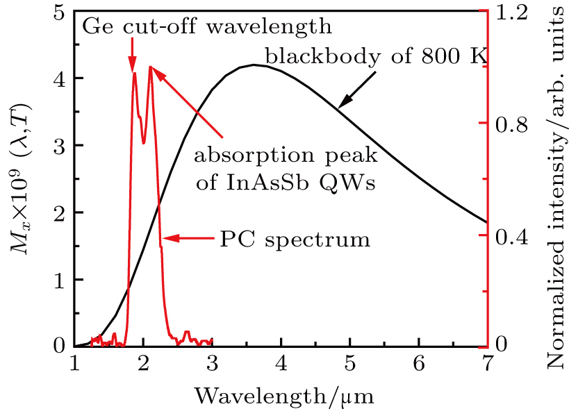
The typical normalized relative spectral response curve is tested by a Bruker VERTEX 80 Fourier transform infrared spectrometer in Fig. 3 (red solid line). It exhibits two peaks in the photocurrent (PC) spectrum. The left peak is attributed to the GaSb barrier, which is cut off by the Ge window ( at 300 K), and the right one is the interband absorption peak of InAsSb QWs. As shown in Fig. 3, the photodetector has a narrow response range from to with a peak around , which is almost in accordance with the band calculation.

Fig. 3. (color online) Typical normalized relative photocurrent spectral response curves of InAsSb/GaSb QWs (red solid line) with a peak around and blackbody radiation spectrum at 800 K (black solid line).

The blackbody responsivity (Rbb) of the photodetector is measured using a blackbody signal test system. The 800-K blackbody emission spectrum is shown in Fig. 3 (black solid line). The power of incident light onto the device surface is 5.77×10⁻⁷ W calculated based on the equation

where σ is the Stefan–Boltzmann constant, Tb is the temperature of the blackbody, TD is the temperature of the environment, Ab is the aperture of the radiation, AD is the area of the detector, and L is the length between the blackbody and the detector.

Due to the narrow range of the spectral response of the photodetector and the deviation from the peak of the blackbody radiation at 800 K, the value of Rbb is obtained to be 9 mA/W under −500 mV applied bias voltage at an environmental temperature of 300 K. The peak responsivity (Rpeak) is calculated to be 0.4 A/W, corresponding to a quantum efficiency of 23.8% in the case without an anti-reflection coating. Since the total absorption thickness is 50 nm, the absorption coefficient is calculated to be 5.43×104 cm−1 under −500 mV applied bias voltage, which is one order of magnitude higher than that of the InAs/GaSb superlattice p–i–n photodetector.[30] Considering the mismatch between the responding wavelength and the blackbody spectrum, the Rbb can be further increased through arranging InAsSb QWs with different well thickness values and antimony composition to better fit the black body spectrum.

Dark current is one of the critical factors that determine the operating temperature of photodetector. Figure 4(a) shows the plots of dark current density vs. applied bias voltage of the photodetector at different temperatures ranging from 100 K to 300 K. At 300 K, the dark current density is 6.05×10⁻³ A/cm2 under −400 mV applied bias voltage, which is better than the recently reported result by Haddadi et al.[11] The photodetector presents a dark current density of 3.25×10⁻⁵ A/cm2 under zero applied bias voltage at 300 K, which is comparable to the “Rule 07” (1.72×10⁻⁵ A/cm2), a simple empirical relationship, conveniently estimating the dark current of the state-of-the-art HgCdTe photodetector.[31]

Fig. 4. (color online) (a) Dark current densities versus applied bias voltage of the photodetector for different temperatures. (b) Dark current density of the photodetector versus inverse temperature under −400-mV applied bias voltage. The blue line refers to fitting to data in the temperature range between 250 K and 300 K, and the green line represents fitting to data in the temperature range between 100 K and 250 K. (c) Johnson noise limited detectivity of the photodetector measured under different applied bias voltages at a temperature of 300 K.

The dark current characteristic of the sample shows an excellent performance at 300 K, but the measured results at variable temperatures are different. As seen in Fig. 4(b), the dark current decreases rapidly when temperature declines from 300 K to 250 K. The decrease can be attributed to the suppression of diffusion current, which is dominant in this temperature region. However, with the further decrease of temperature, the dark current declines slowly. It can be ascribed to that the diffusion current is suppressed and the GR current is the main constituent of dark currents when temperature is below 250 K. Thus the results indirectly indicate that there are many microscopic defects in the epitaxial layers, which form recombination centers causing the GR current though the material to have no macroscopic defects. There is still room for optimizing the growth procedure to improve the material quality.

As an important figure-of-merit of photodetectors, the Johnson noise limited detectivity of the photodetector is calculated from the following equation:

where η is the peak quantum efficiency, e is the electron charge, Id is the dark current, h is the Planck constant, and ν is the frequency of the incident photon. The calculated dependent on bias voltage is shown in Fig. 4(c). The peak detectivity is under zero bias voltage at 300 K.

The InAsSb/GaSb QWs material system is chosen because of its peculiar type-II energy band structure and excellent limit to dark current. Besides, based on the theoretical calculation, the response range is tunable and it covers the eSWIR, MWIR and LWIR spectrum region with different antimony quantities and well widths. So it is very promising to fabricate the photodetectors covering with which the detector operates at high temperature. With future work on optimizing material quality, parameters of p–n junction and QW bandgap, InAsSb/GaSb QWs photodetectors based on interband transition can be another good candidate for IR detection.

4. Conclusions

In this work, we design, grow, and characterize the InAsSb/GaSb QW photodetectors based on interband transition. Through theoretical calculation, the transition energy of 5-nm thick InAs0.91Sb0.09 embedded in the GaSb barrier can be shortened to a value corresponding to a wavelength of . The photodetector exhibits a narrow response range from to with a peak around at 300 K. The peak responsivity is 0.4 A/W under −500-mV applied bias voltage, corresponding to a peak quantum efficiency of 23.8%. The peak detectivity is under zero bias voltage at 300 K in the case without any anti-reflection coating. The photodetector presents a dark current density of 6.05×10⁻³ A/cm2 and 3.25×10⁻⁵ A/cm2 under −400 mV and zero applied bias voltage, separately. Although there is still room for further optimizing those results, they are already better than those of current III/V IR detectors and comparable to those of state-of-the-art HgCdTe detectors.

Acknowledgment

We thank the Laboratory of Microfabrication, Institute of Physics, Chinese Academy of Sciences for fabricating the devices.

Reference
1 Levine B F 1993 J. Appl. Phys. 74 R1
2 Norton P 2002 Opto.-Electron Rev. 10 159
3 Rodriguez J B Plis E Bishop G Sharma Y D Kim H Dawson L R Krishna S 2007 Appl. Phys. Lett. 91 043514
4 Rogalski A 2009 Acta Physica Polonica 116 389
5 Rogalski A 2003 Prog. Quantum Electron. 27 59
6 Rogalski A 2011 Infrared Phys. Technol. 54 136
7 Piotrowski J Rogalski A 2004 Infrared Phys. Technol. 46 115
8 Piotrowski J Galus W Grudzien M 1991 Infrared Phys. 31 1
9 Jiang L Li S S Yeh N T Chyi J I Ross C E Jones K S 2003 Appl. Phys. Lett. 82 1986
10 Bhattacharya P Su X H Chakrabarti S Ariyawansa G Perera A G U 2005 Appl. Phys. Lett. 86 191106
11 Haddadi A Chevallier R Dehzangi A Razeghi M 2017 Appl. Phys. Lett. 110 101104
12 Karimi M Jain V Heurlin M Nowzari A Hussain L Lindgren D Stehr J E Buyanova I A Gustafsson A Samuelson L Borgstrom M T Pettersson H 2017 Nano Lett. 17 3356
13 Madejczyk P Gawron W Piotrowski A Kłos K Rutkowski J Rogalski A 2011 Infrared Phys. Technol. 54 310
14 Piotrowski A Madejczyk P Gawron W Kłos K Pawluczyk J Rutkowski J Piotrowski J Rogalski A 2007 Infrared Phys. Technol. 49 173
15 Martyniuk P Kozniewski A Keblowski A Gawron W Rogalski A 2014 Opto.-Electron Rev. 22 118
16 Rogalski A 2005 Rep. Prog. Phys. 68 2267
17 Maimon S Wicks G W 2006 Appl. Phys. Lett. 89 151109
18 Baril N Brown A Maloney P Tidrow M Lubyshev D Qui Y Fastenau J M Liu A W K Bandara S 2016 Appl. Phys. Lett. 109 122104
19 Kopytko M Wrobel J Jozwikowski K Rogalski A Antoszewski J Akhavan N D Umana-Membreno G A Faraone L Becker C R 2015 J. Electron. Mater. 44 158
20 Kopytko M 2014 Infrared Phys. Technol. 64 47
21 Gautam N Myers S Barve A V Klein B Smith E P Rhiger D R Dawson L R Krishna S 2012 Appl. Phys. Lett. 101 021106
22 Martyniuk P Rogalski A 2013 Opto.-Electron Rev. 21 239
23 Lao Y F Perera A G U Li L H Khanna S P Linfield E H Liu H C 2014 Nat. Photon. 8 412
24 Wang W Wang L Jiang Y Ma Z Sun L Liu J Sun Q Zhao B Wang W Liu W Jia H Chen H 2016 Chin. Phys. 25 097307
25 Yang H Ma Z Jiang Y Wu H Zuo P Zhao B Jia H Chen H 2017 Sci. Rep. 7 43357
26 Sun Q L Wang L Jiang Y Ma Z G Wang W Q Sun L Wang W X Jia H Q Zhou J M Chen H 2016 Chin. Phys. Lett. 33 106801
27 Liu J Wang L Jiang Y Ma Z G Wang W Q Sun L Jia H Q Wang W X Chen H 2017 J. Infrared Millim. Waves 36 129
28 Woolley J C Warner J 1964 Can. J. Phys. 42 1879
29 Sun Q L Wang L Wang W Q Sun L Li W C Wang W X Jia H Q Zhou J M Chen H 2015 Chin. Phys. Lett. 32 106801
30 Walther M Schmitz J Rehm R Kopta S Fuchs F Fleissner J Cabanski W Ziegler J 2005 J. Cryst. Growth 278 156
31 Tennant W E Lee D Zandian M Piquette E Carmody M 2008 J. Electron. Mater. 37 1406