Direct observation of melted Mott state evidenced from Raman scattering in 1T-TaS2 single crystal
Hu Qing1, Yin Cong1, Zhang Leilei2, Lei Li2, ‡, Wang Zhengshang1, Chen Zhiyu1, Tang Jun1, 3, Ang Ran1, 3, †
Key Laboratory of Radiation Physics and Technology, Ministry of Education, Institute of Nuclear Science and Technology, Sichuan University, Chengdu 610064, China
Key Laboratory of High Energy Density Physics and Technology, Ministry of Education, Institute of Atomic and Molecular Physics, Sichuan University, Chengdu 610065, China
Institute of New Energy and Low-Carbon Technology, Sichuan University, Chengdu 610065, China


† Corresponding author. E-mail: rang@scu.edu.cn lei@scu.edu.cn

Project supported by the National Natural Science Foundation of China (Grant Nos. 51771126 and 11774247), the Youth Foundation of Science and Technology Department of Sichuan Province, China (Grant No. 2016JQ0051), and the World First-Class University Construction Funding.

Abstract

The evolution of electron correlation and charge density wave (CDW) in 1T-TaS2 single crystal has been investigated by temperature-dependent Raman scattering, which undergoes two obvious peaks of A1g modes about 70.8 cm−1 and 78.7 cm−1 at 80 K, respectively. The former peak at 70.8 cm−1 is accordant with the lower Hubbard band, resulting in the electron-correlation-driven Mott transition. Strikingly, the latter peak at 78.7 cm−1 shifts toward low energy with increasing the temperature, demonstrating the occurrence of nearly commensurate CDW phase (melted Mott phase). In this case, phonon transmission could be strongly coupled to commensurate CDW lattice via Coulomb interaction, which likely induces appearance of hexagonal domains suspended in an interdomain phase, composing the melted Mott phase characterized by a shallow electron pocket. Combining electronic structure, atomic structure, transport properties with Raman scattering, these findings provide a novel dimension in understanding the relationship between electronic correlation, charge order, and phonon dynamics.

1. Introduction

Coexistence, competition, and collaboration of electron correlation with charge order or charge-density-wave (CDW) are a long-term unresolved issue in low dimensional physics. While the CDW order is well understood by the conventional Peierls mechanism in terms of Fermi-surface nesting due to electron–phonon coupling, electron correlation also plays a crucial role as well in some circumstances.[14] Layered transition-metal dichalcogenides (TMDs)[58] provide an ideal platform for investigating the interplay in that their intrinsic two-dimensional structure is susceptible to electronic instability. Among many TMDs, it has attracted much attention in 1T-TaS2, where its CDW phases include nearly commensurate CDW (NCCDW) and commensurate CDW (CCDW) phases. Additionally, its CCDW phase is compatible to the Mott insulating phase because of the strong electron–phonon and electron–electron interactions.[913]

Current explanation of 1T-TaS2 and its associated phases, which is focused mainly on electronic states, can be summarized in four aspects: (i) Ta atoms are displaced to form star-of-David clusters where 12 Ta atoms contract toward a central Ta atom, interlocking each cluster to form a triangular superlattice.[9,10,14] However, the 12 electrons dominate the states below the distortion-induced gap and the thirteenth one occupies the states above the gap, leading to a Mott insulating state which is responsible for high resistivity of the CCDW phase.[1517] (ii) The neighbouring NCCDW phase contains the star-of-David clusters, although they are less uniformly arranged.[9] (iii) Upon increasing temperature, the Mott phase melts into the NCCDW phase (the melted Mott phase) with an extremely fast charge response and a sudden resistivity drop, where several tens of stars organize into roughly hexagonal domains.[12,18] These reproduce locally the CCDW Mott phase, revealing that the CCDW mechanism is beyond the framework of the conventional Peierls picture.[1922] (iv) The CCDW superlattice structure could be described by the trigonal structure due to the weak interlayer interaction.[23,24] Definitely, none of them have verified a seemly counter-intuitive origin in understanding the low-dimensional electron system.

In this work, we provide definitive evidence that electron-correlation-driven Mott transition and NCCDW transition (melted Mott transition) can be directly confirmed by Raman scattering in 1T-TaS2. The observed melted Mott phase reflected by a shallow electron pocket, i.e., likely hexagonal domains which pinned in an interdomain phase, could originate from strong coupling between phonon excitation and CCDW lattice. Combining the microstructure, transport properties, electronic structure with Raman scattering, the findings presented here may provide insight into approaches for manipulating various CDW phases to understand underlying physics in low-dimensional electron systems.

2. Experimental procedure

High-quality single crystals of 1T-TaS2 was grown by the chemical vapor transport technique with iodine as a transport agent. The temperature dependence of resistivity and Seebeck coefficient were carried out using a standard four-probe configuration in a quantum design physical properties measurement system (PPMS). Thin-foil specimens for transmission electron microscopy (TEM) and scanning TEM (STEM) imaging were prepared by cutting single crystal from [0001] (c axis). The selected-area diffraction pattern (SADP) and TEM images were taken using the JEOL JEM-2010 F electron microscope operated at 200 kV. The high-angle annular dark-field (HAADF) and annular bright-field (ABF) images were taken with a 200-kV ARM-200FC STEM equipped with a probe corrector (CEOS Gmbh). Raman scattering spectra were recorded through a custom-built Raman system using a triple grating monochromator (Andor Shamrock SR-303i-B, EU) with an attached electron-multiplying CCD (ANDOR Newton DU970P-U VB, EU) excited with a 532 nm solid-state laser (RGB laser system, Germany). Low-temperature Raman experiments were performed with the Freezing Stage (THMS600, UK). Angle-resolved photoemission spectroscopy (ARPES) measurements were performed using a VG-SCIENTA SES2002 spectrometer with a high-flux He discharge lamp. The He–Iα ( = 21.218 eV) resonance line was used to excite photoelectrons.

3. Experimental results and discussion

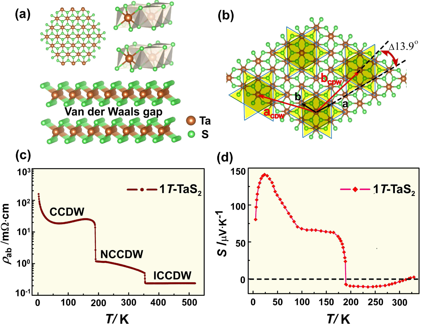
Figure 1(a) shows sketches of its crystal structure and atomic planes in 1T-TaS2, in which the central Ta is octahedrally coordinated by six S atoms within the P-3m1 space group. One plane of the hexagonally arranged Ta atoms is sandwiched in between two planes of the hexagonally packed S atoms by weak van der Waals interactions, while they are covalently bonded within the TMD sheets.[9] Figure 1(b) shows each cluster interlocked by forming a triangular superlattice with a periodicity.[9,10,14] The temperature dependence of in-plane resistivity ρab is shown in Fig. 1(c). A first-order transition from the NCCDW to the CCDW phase is discovered below 200 K. To shed light on the species of carriers, thermoelectric power S as a function of temperature is presented as shown in Fig. 1(d). The transition of S follows the one from NCCDW to CCDW phase, in agreement with the transition of resistivity. Interestingly, the sign of S is altered and switches from negative to positive in the vicinity of the transition, indicating that the charge carriers change from electron type (n-type) to hole type (p-type). Below the temperature of NCCDW transition, more hole carriers dominate the transport properties, which exhibits large Seebeck coefficient at low temperatures.

Fig. 1. (color online) (a) Crystal structure of 1T-TaS2. (b) Commensurate CDW (CCDW) triangular superlattice. The black and red arrows indicate the lattice vectors of 1 × 1 and superstructure, respectively. (c), (d) Temperature dependence of in-plane resistivity (ρab) and thermoelectric power S, respectively.

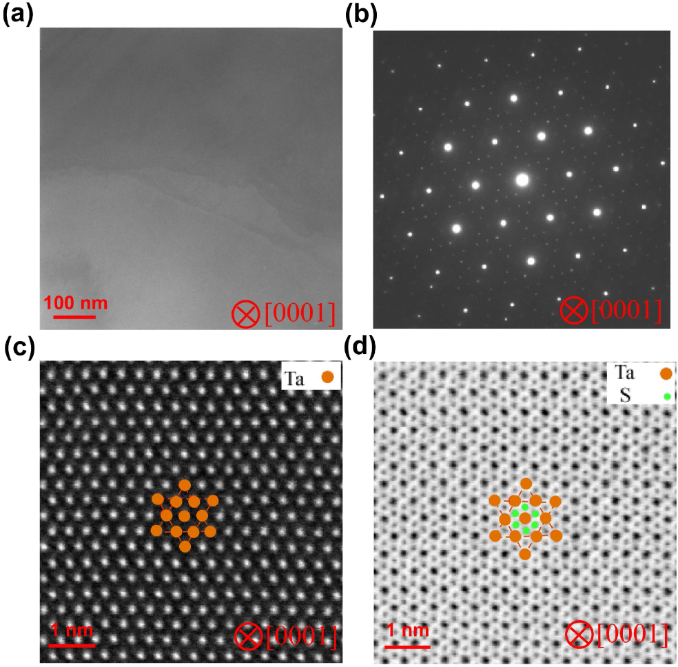
To examine the microstructure of 1T-TaS2, we performed TEM and SADP observed from [0001] orientation as shown in Figs. 2(a) and 2(b). The atomically thin flake of 1T-TaS2 displays a uniform and smooth surface. The SADP with six-fold rotational symmetry confirms the hexagonal structure of 1T-TaS2. In order to obtain high-resolution atomic structure further, the HAADF and ABF STEM viewed along c axis at room temperature have been indicated in Figs. 2(c) and 2(d). Since intensity of an atomic column in a HAADF imaging mode is proportional to Z1.7 (Z is atomic number),[25] the brighter spots represent the Ta columns. Evidently, Ta atoms (marked by larger orange circles) are almost located at the identical sites in all cases, forming the star-of-David clusters, where stars are interlocked by forming a triangular superlattice with a periodicity, in line with the crystal structure (see Figs. 1(a) and 1(b)). Surprisingly, only Ta atoms are visible in the HAADF image, whereas S atoms cannot be identified (Fig. 2(c)). Taking into account the fact that the much lighter S atoms are not scattered strongly enough to be visualized thus posing a significant hurdle to obtaining a complete structural configuration in terms of the HAADF STEM interpretation alone. To directly resolve all atomic columns, we take our newly developed ABF STEM imaging technique to observe 1T-TaS2. The ABF STEM approach has been demonstrated to allow a simultaneous imaging of light and heavy atoms with a good signal-to-noise ratio, robustly over a range of sample thickness.[26] Apart from conveying fundamental structural information as in the HAADF, the ABF STEM image, in which the dark spots represent atomic columns, identifies additional spots with weaker image contrast (smaller green circles) as the S columns (Fig. 2(d)), verifying the power of ABF technique.

Fig. 2. (color online) (a) Low-resolution TEM image and (b) the corresponding SADP patters of 1T-TaS2 along [0001] projection uncover the evident 6-fold rotational symmetry. (c) Atom-resolved HAADF and (d) ABF STEM images seen from [0001] projection (c axis). Brighter spots represent Ta atomic columns (larger orange circles), while darker ones S atomic columns (smaller green circles).

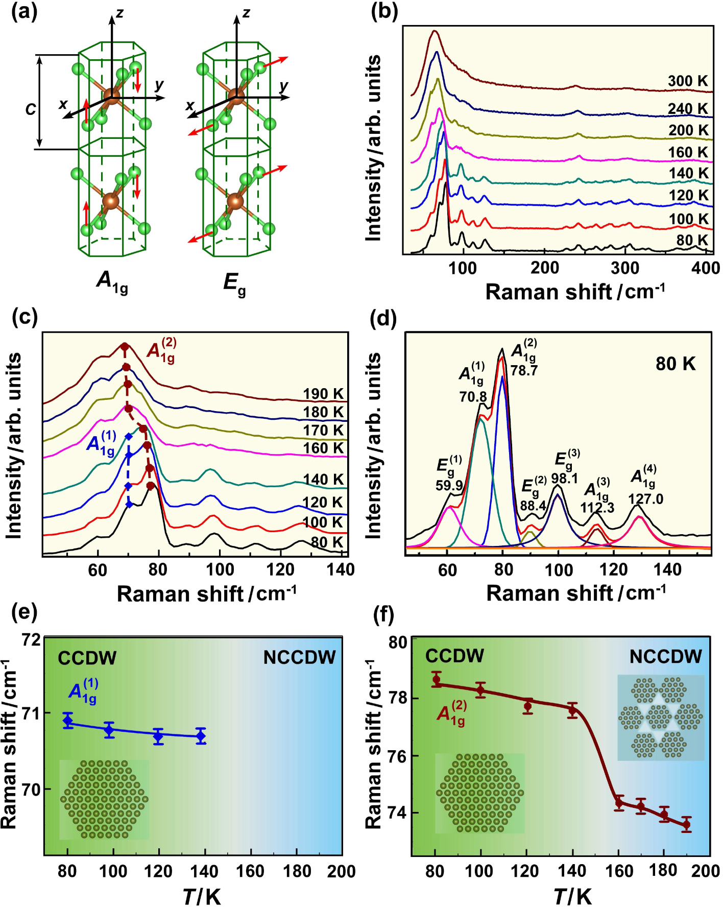
To track the dynamical properties of lattice vibrations, we carried out Raman scattering measurements. There are two Raman-active phonon modes including A1g and Eg modes,[2729] in which A1g mode refers to two S atoms per unit cell move relative to one another along z orientation, while a doubly-degenerate Eg mode reflects S atoms move opposite to one another along x or y orientation, as plotted in the inset of Fig. 3(a). Figure 3(b) shows the temperature-dependent Raman spectra of 1T-TaS2. The modes with energies below 140 cm−1 as reflected by Fig. 3(c) should arise from acoustic phonon branches where vibration of Ta atoms dominates, while those above 220 cm−1 originate from optical branches where vibration of S atoms presides. It is found that 70.8, 78.7, 112.3, 127.0 cm−1 of the pronounced out-of-plane A1g modes and 59.9, 88.4, 98.1 cm−1 of in-plane Eg modes are clearly observed at 80 K in the CCDW phase, defined as in Fig. 3(d). Especially for the two distinct peaks of and based on most remarkable intensity (i.e., 70.8 and 78.7 cm−1), the peak at 70.8 cm−1 is nearly temperature-independent in the CCDW phase and completely disappears above 160 K as plotted in Figs. 3(c) and 3(e). Such results reveal the Mott-Hubbard gap opening, which is triggered by enhancement of effective electron correlation.[11,16,22] The CCDW phase is composed of interlocking star-of-David (see Fig. 3(e)). The peak at 78.7 cm−1 apparently shifts toward low energy as the temperature increases. The abrupt transition at ~ 150 K demonstrates that the Mott phase melts into the NCCDW phase (the melted Mott phase) as plotted in Fig. 3(f), indicative of the NCCDW gap opening.[30,31] The melted Mott phase could be visualized as hexagonal domains suspended in an interdomain phase (see Fig. 3(f)).

Fig. 3. (color online) (a) Two main types of crystal lattice Raman-active vibration A1g and Eg modes in 1T-TaS2. (b) Temperature-dependent Raman spectra in the cooling cycle from 300 to 80 K. (c) Temperature-dependent Raman spectra focused on the temperature range from 190 to 80 K. (d) All of fitting peaks derived from Raman spectra at 80 K. (e), (f) Shift of Raman peaks of and as a function of temperature, respectively. Evolution of superstructure illustrated from CCDW to NCCDW phase based on Raman spectra.

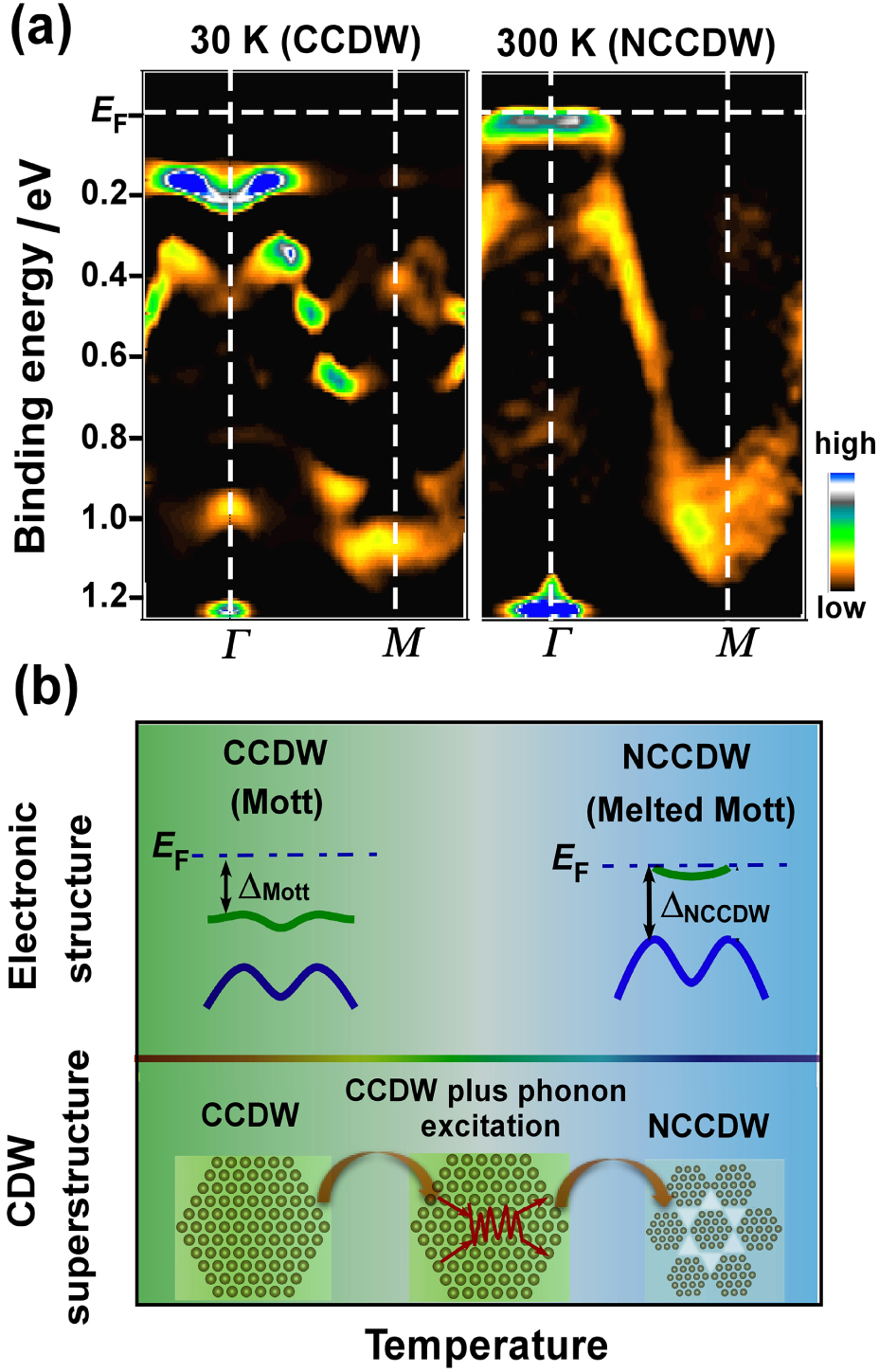
To gain more insights into correlation between CCDW (Mott phase), NCCDW (melted Mott phase), electronic structure, and phonon transmission, we performed band dispersions based on ARPES along the ΓM cut measured at 30 K (Mott phase) and 300 K (melted Mott phase) as shown in Fig. 4(a). In the Mott phase at 30 K, the Ta 5d band splits into multiple subbands because of strong CDW potential. Also, near Fermi surface (EF) spectral weight resides on the higher binding energy (EB) side of ~ 0.2 eV which originates from Mott transition and is assigned as the low Hubbard band (LHB).[17,32] In the NCCDW phase at 300 K, a highly dispersive band does not cross EF but disperses back toward higher EB near the κF (Fermi vector) point, with a characteristic pseudogap (NCCDW gap) feature. Such band-folding behavior and ARPES-intensity modification are likely caused by the superlattice potential of the NCCDW where the star-of-David clusters locally maintain the periodicity identical to the CCDW Mott phase. Inside the NCCDW gap, a narrow band pinned at EF is also observed around the Γ point. Furthermore, the narrow band is verified as an intrinsic electron pocket across EF.[31,33]

Fig. 4. (color online) (a) Second-derivative ARPES intensity of 1T-TaS2 plotted as a function of wave vector and binding energy at 30 K and 300 K, respectively. (b) Schematic band diagram derived from the ARPES experiment and evolution of superstructure from CCDW to NCCDW phase before and after phonon excitation as a function of temperature.

Figure 4(b) summarizes the band picture and phonon excitations in the CCDW and NCCDW phases, respectively. The shallow electron pocket appears in the NCCDW phase (melted Mott phase). This pocket is gapped in the Mott phase due to the enhanced electron correlation. In other words, the shallow electron pocket transforms into the LHB in the Mott phase further reveals an intimate link between the electron correlations, CCDW state, and NCCDW state. With increasing temperature, more phonons could be excited and coupled to CCDW lattice by Coulomb interaction, evidenced from observed Raman shift (see Fig. 3(f)). Therefore, the phonon propagation would result in corresponding fluctuations of CCDW state, which could cause the emergence of hexagonal domains suspended in the interdomain phase, forming the NCCDW state (melted Mott state) characterized by the shallow electron pocket (see Fig. 4(b)). The strongly coupled CCDW–phonon excitations would trigger large Raman intensity, in line with the experiment of Raman scattering (Figs. 3(b)3(d)). The direct observation of charge-order transition from Raman scattering represents an important step forward in fully tailoring the CCDW phase (Mott insulating phase) and NCCDW phase.

4. Conclusion

We have reported the temperature dependence of Raman scattering in layered 1T-TaS2 single crystal. We found direct evidence for electron-correlation-driven Mott transition and NCCDW transition (melted Mott transition) derived from Raman scattering. The electronic structure demonstrates that the shallow electron pocket is responsible for the melted Mott phase, where the possible hexagonal domains pinned in the interdomain phase, revealing strong coupling between phonon excitation and CCDW lattice. The present results not only render to recognize the intrinsic origin of Mott and NCCDW phases, but also provide a deep insight into close association between electronic correlation, charge-order state, and dynamical motions of phonons.

Reference
[1] Mathur N D Grosche F M Julian S R Walker I R Freye D M Haselwimmer R K M Lonzarich G G 1998 Nature 394 39
[2] Lefebvre S Wzietek P Brown S Bourbonnais C Jérome D Mézière C Fourmigué M Batail P 2000 Phys. Rev. Lett. 85 5420
[3] Dagotto E 1994 Rev. Mod. Phys. 66 763
[4] Damascelli A Hussain Z Shen Z X 1994 Rev. Mod. Phys. 75 473
[5] Mattheiss L F 1973 Phys. Rev. 8 3719
[6] Gabovich A M Voitenko A I Ausloos M 2002 Phys. Rep. 367 583
[7] Wang H T Li L J Ye D S Cheng X H Xu Z A 2007 Chin. Phys. 16 2471
[8] Yang H T Tao H J Zhang Z X 1998 Chin. Phys. Lett. 15 123
[9] Wilson J A Di Salvo F J Mahajan S 1975 Adv. Phys. 24 117
[10] Fazekas P Tosatti E 1979 Philos. Mag. 39 229
[11] Manzke R Buslaps T Pfalzgraf B Skibowski M Anderson O 1989 Europhys. Lett. 8 195
[12] Thomson R E Burk B Zettl A Clarke J 1994 Phys. Rev. 49 16899
[13] Pillo T Hayoz J Berger H Fasel R Schlapbach L Aebi P 2000 Phys. Rev. 62 4277
[14] Scruby C B Williams P M Parry G S 1975 Philos. Mag. 31 255
[15] Rossnagel K Smith N V 2006 Phys. Rev. 73 073106
[16] Smith N V Kevan S D Disalvo F J 1985 J. Phys. 18 3175
[17] Zwick F Berger H Vobornik I Margaritondo G Forró L Beeli C Onellion M Panaccione G Taleb-Ibrahimi A Grioni M 1998 Phys. Rev. Lett. 81 1058
[18] Spijkerman A de Boer J L Meetsma A Wiegers G A van Smaalen S 1997 Phys. Rev. 56 13757
[19] Hellmann S Beye M Sohrt C Rohwer T Sorgenfrei F Redlin H Kalläne M Marczynski-Bühlow M Hennies F Bauer M Föhlisch A Kipp L Wurth W Rossnagel K 2010 Phys. Rev. Lett. 105 187401
[20] Eichberger M Schäfer H Krumova M Beyer M Demsar J Berger H Moriena G Sciani G Miller R J D 20D Nature 468 799
[21] Ishizaka K Kiss T Yamamoto T Ishida Y Saitoh T Matsunami M Eguchi R Ohtsuki T Kosuge A Kanai T Nohara M Takagi H Watanabe S Shin S 2011 Phys. Rev. 83 081104
[22] Petersen J C Kaiser S Dean N Simoncig A Liu H Y Cavalieri A L Cacho C Turcu I C E Springate E Frassetto F Poletto L Dhesi S S Berger H Cavalleri A 2011 Phys. Rev. Lett. 107 177402
[23] Sugai S Murase K Uchida S Tanaka S 1981 Physica B+C 105 405
[24] Duffey J R Kirby R D Coleman R V 1976 Solid State Commun. 20 617
[25] Pennycook S J Boatner L A 1988 Nature 336 565
[26] Findlay S D Shibata N Sawada H Okunishi E Kondo Y Yamamoto T Ikuhara Y 2009 Appl. Phys. Lett. 95 191913
[27] Uchida S Sugai S 1981 Physica B+C 105 393
[28] He R Okamoto J Ye Z P Ye G H Anderson H Dai X Wu X X Hu J P Liu Y Lu W J Sun Y P Pasupathy A N Tsen A W 2016 Phys. Rev. 94 201108
[29] Albertini O R Zhao R McCann R L Feng S M Terrones M Freericks J K Robinson J A Liu A Y 2016 Phys. Rev. 93 214109
[30] Pillo Th Hayoz J Berger H Grioni M Schlapbach L Aebi P 1999 Phys. Rev. Lett. 83 3494
[31] Ang R Tanaka Y Ieki E Nakayama K Sato T Li L J Lu W J Sun Y P Takahashi T 2012 Phys. Rev. Lett. 109 176403
[32] Perfetti L Loukakos P A Lisowski M Bovensiepen U Berger H Biermann S Cornaglia P S Georges A Wolf M 2006 Phys. Rev. Lett. 97 067402
[33] Ang R Miyata Y Ieki E Nakayama K Sato T Liu Y Lu W J Sun Y P Takahashi T 2013 Phys. Rev. 88 115145