


Formation of high-Sn content polycrystalline GeSn films by pulsed laser annealing on co-sputtered amorphous GeSn on Ge substrate
Cite this Article
Zhang Lu, Hong Hai-Yang, Wang Yi-Sen, Li Cheng, Lin Guang-Yang, Chen Song-Yan, Huang Wei, Wang Jian-Yuan. Formation of high-Sn content polycrystalline GeSn films by pulsed laser annealing on co-sputtered amorphous GeSn on Ge substrate. Chinese Physics B, 2017, 26(11): 116802 
Permissions
Formation of high-Sn content polycrystalline GeSn films by pulsed laser annealing on co-sputtered amorphous GeSn on Ge substrate
† Corresponding author. E-mail:
Project supported by the National Natural Science Foundation of China (Grant No. 61474094) and the National Basic Research Program of China (GrantNo. 2013CB632103).
Abstract
Polycrystalline Ge1−x (poly-Ge1−xSnx) alloy thin films with high Sn content (> 10%) were fabricated by cosputtering amorphous GeSn (a-GeSn) on Ge (100) wafers and subsequently pulsed laser annealing with laser energy density in the range of 250 mJ/cm2 to 550 mJ/cm2. High quality poly-crystal Ge0.90Sn0.10 and Ge0.82Sn0.18 films with average grain sizes of 94 nm and 54 nm were obtained, respectively. Sn segregation at the grain boundaries makes Sn content in the poly-GeSn alloys slightly less than that in the corresponding primary a-GeSn. The crystalline grain size is reduced with the increase of the laser energy density or higher Sn content in the primary a-GeSn films due to the booming of nucleation numbers. The Raman peak shift of Ge–Ge mode in the poly crystalline GeSn can be attributed to Sn substitution, strain, and disorder. The dependence of Raman peak shift of the Ge–Ge mode caused by strain and disorder in GeSn films on full-width at half-maximum (FWHM) is well quantified by a linear relationship, which provides an effective method to evaluate the quality of poly-Ge1−xSnx by Raman spectra.
1. Introduction
Ge1−xSnx alloys with Sn content higher than about 0.1 are revealed to achieve the transition from indirect to direct band gap.[1–3] Therefore, single crystalline Ge1−xSnx have been intensively studied[4,5] as promising materials for light emitting devices[6,7] based fully on group IV elements. In addition, GeSn lasers have been reported[8–10] as the solution to the problem of a lack of monolithic Si-based laser sources. With high carrier mobility exceeding 500 cm2/(V⋅s),[11] GeSn can be used for high performance complementary metal-oxide-semiconductor (CMOS) devices.[11–13] All of the above need high-quality single crystalline Ge1−xSnx which must meet strict growth conditions. On the other hand, relatively few studies of poly-GeSn which have significant potential for the use in thin film transistors (TFTs) and infrared focal plane array (IRFPA) detectors have been reported.[14,15] Furthermore, the characterization and analysis of disorder in poly-GeSn have scarcely been reported. Therefore, the processing and analysis techniques of poly-GeSn films with large grain size and high Sn content have important values.
High-Sn content poly-GeSn reveals lower crystallization temperature below 400 °C[16,17] and thermal conductivity about 5–9 W⋅m−1·K−1,[17] which is a suitable channel material for high-performance TFTs rather than poly-Si. It even potentially provides a material platform for better performance flexible TFTs. However, the low solid solubility of α-Sn in Ge below 1 at.%[18,19] hinders the development of high-Sn content GeSn. In order to overcome this problem, non-equilibrium techniques such as pulsed laser annealing (PLA) have been extensively used.[20,21] The PLA process provides a local and rapid annealing source and then cools down in an ultra-short time scale of nanoseconds, which is much shorter as compared to rapid thermal annealing (RTA). Besides, PLA can confine the thermally affected zone in the vicinity of the laser treated area. Thus, high crystallinity and high Sn content GeSn can be achieved by PLA.
In this work, we deposit a-GeSn on p-type Ge (100) wafer with 0.088 Ω·cm resistivity by magnetron sputtering and then transform it into poly-GeSn with large grain size (50–94 nm) and high Sn content (10%–18%) using PLA. The GeSn grain size is found to be reduced with the increase of the laser energy density or higher Sn content in the initial a-GeSn. Disorder of poly-crystal GeSn alloys, besides Sn content and strain, has a great impact on the Raman peak shift of Ge–Ge mode. The influence of the energy density of PLA and the Sn content in the initial a-GeSn on the properties of the poly-crystal GeSn is discussed in detail.
2. Experimental procedure
The processes of sample preparation are schematically shown in Fig.
 | Fig. 1. (color online) Fabrication scheme of poly-GeSn films. |
The crystalline phase and Sn content in the samples were characterized by x-ray diffraction (XRD) patterns and selected-area electron diffraction (SAED) patterns. The depth analysis of chemical composition of poly-GeSn by Auger electron spectroscopy (AES) illuminated that the Sn segregation is neither on the surface nor at the interface between the poly-GeSn and buffer-Ge but at the grain boundaries. Transmission electron microscopy (TEM) was used for structural characterization. After etching off the segregated Sn by HCl solution for 3 min, the poly-GeSn grains were visibly observed by scanning electron microscopy (SEM). Additionally, disorder in poly-GeSn which lost long-range orders was analyzed by Raman scattering spectroscopy (spot size: 4 μm, wavelength: 532 nm).
3. Results and discussion
Figure
 | Fig. 2. (color online) XRD patterns of poly-Ge and poly-GeSn films fabricated from (a) a-Ge0.85Sn0.15 and (b) a-Ge0.8Sn0.2 after PLA with energy density of 250 mJ/cm2, 400 mJ/cm2, and 550 mJ/cm2. |
| Table 1. Sn contents for poly-Ge1−xSnx films fabricated from samples a-Ge0.85Sn0.15 and -Ge0.8Sn0.2 after PLA. The values x1, and x2 are calculated from the diffraction peaks of GeSn (111) and (220) in the XRD patterns, respectively. . |
In order to analyze the disorder in the polycrystalline films by Raman scattering spectroscopy, we have prepared poly-Ge films on Ge (100) wafers with different crystalline qualities using PLA with 250 mJ/cm2 and RTA at 600 °C. Figure
 | Fig. 3. (color online) Raman scattering spectroscopy of samples: (a) as-deposited a-Ge and poly-Ge crystallized by PLA with 250 mJ/cm2 and RTA at 600 °C, (b) a-Ge0.85Sn0.15 and (c) a-Ge0.8Sn0.2 after the PLA process at energy density of 250 mJ/cm2, 400 mJ/cm2, and 550 mJ/cm2. The insets show trends of FWHM and Δω respected to (a) different crystalline qualities and (b), (c) different energy density. (d) The Ge–Ge mode peak shift Δωstrain+disorder in a-Ge and poly-Ge1−xSnx (0 ≤ x ≤ 0.18) caused by strain and disorder depends on FWHM. The dash line is a linear fit to the data. The inset zooms into the data of poly-Ge1−xSnx (0 ≤ x ≤ 0.18). (e) The Ge–Ge mode peak shift Δωstrain+disorder in poly-GeSn films fabricated from a-Ge0.85Sn0.15 and a-Ge0.8Sn0.2 after PLA with energy density of 250 mJ/cm2, 400 mJ/cm2, and 550 mJ/cm2. |
Figures
The depth distribution of chemical elements in the poly-Ge0.85Sn0.15 film formed by PLA on a-Ge0.8Sn0.2 at 250 mJ/cm2 was measured by AES and shown in Fig.
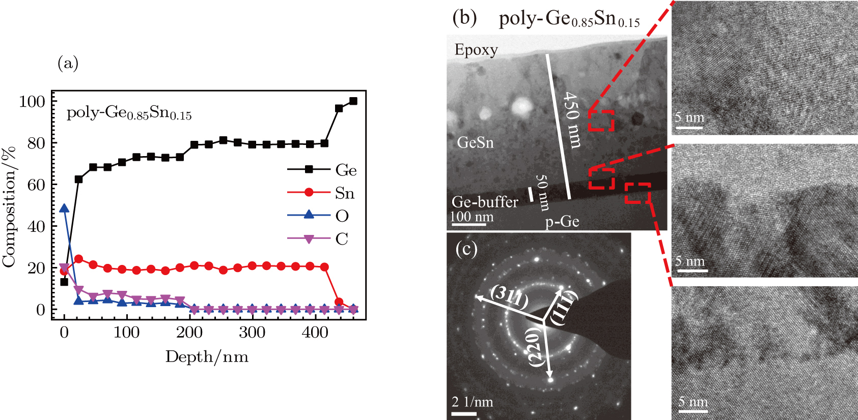 | Fig. 4. (color online) (a) AES scan, (b) TEM image, (c) and SAED patterns of the sample poly-Ge0.85Sn0.15. |
After etching off the segregated Sn at the grain boundaries by HCl solution for 3 min, the poly-GeSn grains were visibly observed in SEM images as shown in Fig.
 | Fig. 5. SEM images of poly-GeSn films fabricated from (a)–(c) a-Ge0.85Sn0.15 and (d)–(f) a-Ge0.8Sn0.2 after PLA with energy density of 250 mJ/cm2, 400 mJ/cm2, and 550 mJ/cm2, respectively. |
4. Conclusion
We demonstrated the growth of poly-Ge1−xSnx films with high Sn content (10%–18%) on Ge substrates using pulsed laser annealing on co-sputtered a-GeSn. It is shown that the crystalline grain size of poly-GeSn decreases with the increase of the laser energy density or Sn content in the primary a-GeSn film, both of which enhance the nucleation of a-GeSn. High crystal quality Ge0.90Sn0.1 and Ge0.82Sn0.18 films with average grain sizes of 94 nm and 54 nm were grown. The uniform distribution of Sn element in depth and SEM images of the etched poly-GeSn films show that Sn segregation occurs at the grain boundaries rather than on the surface or at the interface between the poly-GeSn and buffer-Ge. The dependence of Ge–Ge mode peak shift caused by strain and disorder on FWHM is well quantified by a linear relationship, which commendably provides an effective method to evaluate the quality of poly-Ge1−xSnx by Raman spectra. As poly-Ge can be used for multiple flexible devices such as metal–semiconductor–metal photodiodes,[23] TFTs, and IRFPA,[24] poly-GeSn should be a very promising material to improve the performance of the above devices for the electrical properties enhanced by the doping of Sn into Ge. Hence, further study on high quality GeSn is necessary and significant.
Reference
| [1] | |
| [2] | |
| [3] | |
| [4] | |
| [5] | |
| [6] | |
| [7] | |
| [8] | |
| [9] | |
| [10] | |
| [11] | |
| [12] | |
| [13] | |
| [14] | |
| [15] | |
| [16] | |
| [17] | |
| [18] | |
| [19] | |
| [20] | |
| [21] | |
| [22] | |
| [23] | |
| [24] |