Structural characterization of indium-rich nanoprecipitate in InGaN V-pits formed by annealing
Xue Junjun1, 3, Cai Qing2, Zhang Baohua2, Ge Mei2, Chen Dunjun2, †, Zhi Ting1, Chen Jiangwei1, Wang Lianhui3, Zhang Rong2, Zheng Youdou2
School of Electronic Science and Engineering, Nanjing University of Posts and Telecommunications, Nanjing 210023, China
School of Electronic Science and Engineering, Nanjing University, Nanjing 210093, China
Institute of Advanced Materials, Nanjing University of Posts and Telecommunications, Nanjing 210023, China


† Corresponding author. E-mail: djchen@nju.edu.cn

Project supported by the National Natural Science Foundation of China (Grant Nos. 61604080, 61574079, 61634002, and 61474060), Natural Science Foundation of Jiangsu Province, China (Grant No. BK20160883), University Science Research Project of Jiangsu Province, China (Grant Nos. 16KJB140011 and 14KJB510020), and NUPTSF, China (Grant No. NY214154).

Abstract

InGaN layers capped with GaN were annealed at 550 °C for 1 hour. During annealing, cracks appeared and dissolved InGaN penetrated through the microcracks into the V-pits to form indium-rich nanoprecipitates. Some precipitates, in-situ annealed under nitrogen ion irradiation by MBE, were confirmed to be cubic GaN on the tops of precipitates, formed by nitriding the pre-existing Ga droplets under nitrogen ions irradiation.

1. Introduction

Annealing can reduce hardness, generate phase transition, eliminate defects and residual stress in steel,[1,2] making it the most important processing treatment in metallurgy. These applications of annealing have the same effects on III-nitride semiconductors. Moreover, many researchers have investigated the micro-structural changes of GaN,[3,4] InGaN,[5,6] and InAlN[7] induced by breaking of chemical bonds during annealing. This makes it more attractive to remove the phase separation in rich indium content alloys by annealing.[6,8,9] Besides all that, for GaN related semiconductors, annealing is usually applied to activate dopants[10] and to prepare ohmic contacts.[11]

Though some further achievements on InGaN have been made in recent years,[1214] several barriers still exist in obtaining indium-rich InGaN alloys. The lattice mismatch and gap of miscibility between GaN and InN are the main barriers to obtaining high crystalline quality InGaN with high indium content. In order to overcome these difficulties, more details of InGaN properties and growth mechanisms should be learned. In fact, the results from annealing, for InGaN alloys, depend strongly on the conditions of annealing.[5,6] But all the processes of indium incorporation or decomposition from InGaN have the identical characteristic that the In–N bonds are weaker than the Ga–N bonds. In this work, a novel nanostructure is reported, which can be considered to be a precipitate of InGaN during annealing. To the best of the author’s knowledge, no research concerning indium-rich precipitates with cone shape in V-pits has ever been reported.

2. Experiment

The InGaN structures, shown schematically in Fig. 1, were grown by plasma assisted molecular beam epitaxy (MBE) on c-plane sapphire. The group III fluxes, including high-purity elemental In and Ga, were supplied by effusion cells. Active nitrogen was produced by a radio-frequency (RF) plasma source, using a nitrogen flow rate of about 3 SCCM that resulted in an N-limited growth rate of about 0.8 μm per hour. The onset of sample growth began with a thin AlN nucleation layer at about 800 °C. The growth temperature was lowered to about 700 °C for growth of a GaN buffer layer with thickness of 1 μm and to about 500 °C for growth of an InGaN template layer with thickness of 500 nm. After the growth of InGaN template was complete, the temperature was elevated to 700 °C for growing the GaN capping layer with thickness of 300 nm. The as-grown InGaN films were transferred for annealing procedures. The InGaN sample, called S1, was in-situ annealed at 550 °C under nitrogen ion irradiation by MBE. Another InGaN sample S2 was ex-situ annealed at a temperature of 550 °C in flowing N2 gas under normal atmospheric pressure. The annealing time of both samples was 1 hour.

Fig. 1. (color online) Schematic structure of the InGaN as-grown sample.

Surface morphology was characterized by atomic force microscopy (AFM) and scanning electron microscopy (SEM). Chemical composition was measured by x-ray energy spectrometer (EDS) and cathodoluminescence (CL). Transmission electron microscopy (TEM) was applied to examine the microstructure of the InGaN precipitate.

3. Results and discussion

As shown in Fig. 2(a), besides the rough morphology, many striking deep pits are present on the surface of the as-grown sample. Although the surfaces become flatter after annealing treatments, cracks extent across the entire surface of the samples, and the pits are filled up with nanostructures, as shown in Figs. 1(b) and 1(c). In order to clarify the chemical content of the nano-fillers, EDS tests were applied in and out of the domains of the nano-fillers for both S1 and S2, as shown in Figs. 3(a) and 3(b), respectively. The indium contents obtained by EDS are detailed in Table 1. Hence, the nano-fillers in pits could be considered to be the indium-rich precipitate dissolved out of the InGaN layers during annealing.

Fig. 2. (color online) AFM images of InGaN layers capped with GaN: (a) as-grown, (b) in-situ annealed (S1), (c) ex-situ annealed (S2).
Fig. 3. (color online) SEM images and EDS spectra of annealed samples: (a) S1; (b) S2. The EDS spectra are placed at the bottoms of related SEM images.
Table 1.

Indium contents obtained by EDS at various positions.

.

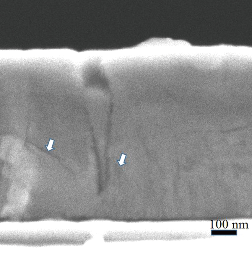
Although this morphology of precipitated phase is very common for alloy aging in metallurgy, it is a rather novel phenomenon for III-nitrides. One formation mechanism for precipitates from alloys is always that after annealing, the grain size in alloys will change and precipitates are deposited in grains along some special directions or on some particular fractures.[15,16] Here, a similar situation is suitable for our samples. This kind of precipitate has an intense relationship with the existence of cracks and, up to now, they are never observed in alloys without cracks. As shown in Fig. 4, besides of the large cracks on the surface, a lot of micro-cracks are generated inside InGaN layers, which were induced by annealing for a long time. The high indium content alloys, extracted from decomposed InGaN, prefer to accumulate in the bottom of pits according to the network of micro-cracks nearby.

Fig. 4. Cross-sectional SEM image of S1.

In fact, the decomposition at an annealing temperature of 550 °C is selective for InN and GaN. That is to say, the In–N bond can be broken very easily, but it is not so easily for the Ga–N bond to decompose into metal gallium at this temperature. So, for S2, an EDS test on position 1*, shown in Fig. 3(b), shows that elemental oxygen is contained in the precipitate. This happens because the O2 in the N2 flow can reach the bottoms of pits through the gap around the precipitates and oxidize the dissolved metal indium during annealing. However, at position 2*, the InGaN layer is protected from the O2 by the stable GaN capping layer and, hence, no elemental oxygen was detected by EDS.

Note that S1 was treated with in-situ annealing and ion irradiation by MBE, which is rarely studied. So, CL measurements were performed to further investigate the structural properties of S1. As shown in Fig. 5, all the precipitates in pits appear as bright emission spots in the CL image, and some spots are much brighter than the others. As the red crosses denote in the CL image, CL spectra taken from spots 1# and 2# are shown in Figs. 5(b) and 5(c). The CL spectrum from the brighter spot 1# reveals the emission peak of 384 nm, while the CL spectrum from spot 2# shows the emission peak centered at 579 nm. It is easy to understand that the origin of 579 nm emission at spot 2# is the In0.37Ga0.63N under the GaN capping layer. But the emission peak of 384 nm could not be from the In0.05Ga0.95N because the indium composition of the underlying InGaN should be much higher than 6% due to the existence of the GaN capping layer and in view of the results of EDS. As reported by Menniger et al., the emission peak of GaN with cubic phase is at 385 nm.[17,18] Here, it is should be mentioned that the distribution of V-pits with nano-fillers is not so uniform in the greater scope, as shown in Fig. 5. As a result, the density of the V-pits could fluctuate broadly at a small spatial scale, exactly as the AFM images show in Figs. 2(b) and 2(c).

Fig. 5. (color online) (a) CL mapping for sample S1. CL spectra extracted from positions of (b) 1# and (c) 2#.

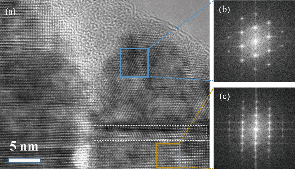
To clarify the origin of 384 nm emission, HRTEM was employed to characterize the precipitates in the pits. It should be mentioned that two crystallographic phases (hexagonal and cubic) are in the precipitate, as shown in Fig. 6. The zinc-blende GaN (z-GaN) is epitaxial on the wurtzitic GaN (w-GaN) and they are confirmed by fast Fourier transform (FFT) patterns from the selected squares inside the z-GaN and w-GaN areas, which are shown in Figs. 6(b) and 6(c), respectively. Actually, the z-GaN phase is distinguished from the w-GaN phase by type II stacking faults, which are highlighted by a white square in Fig. 6(a).[1921] Having a stacking sequence of ... ABABACBCBC..., type II stacking faults possess a displacement of R = 1/3[10-10].[19] Because the stacking fault energy of type II is higher than that of type I (with stacking sequence ... ABABCBCBC...),[19] type II stacking faults are rarely seen in GaN. But, the mixture of both the stable w-GaN and the metastable z-GaN is usually observed in doped GaN (e.g., Zn doping[19] and Mg doping[22,23]) or droplet epitaxial GaN.[24,25] The GaN thin film, for the latter, under nitrogen ion bombardment, exhibits mechanical residual stress, and the ion-induced compressive stress and densification are very high, which may trigger formation of the z-GaN at the beginning of GaN growth.[24,25] In this work, for S1, when growing the GaN capping layer, metal Ga droplets could accumulate at the apex of pits in a Ga-rich condition, and the z-GaN phase could be formed by nitriding the pre-existing Ga droplets under nitrogen ion irradiation. Based on the description above, the z-GaN on the top of precipitates can be considered as the origin of 384 nm emission.

Fig. 6. (color online) (a) HRTEM image of the top of the precipitate of S1. FFT patterns of selected areas in the blue square (b) and the yellow square (c).
4. Conclusion

We have reported a kind of novel nanostructures that filled the pits and are considered to be indium-rich precipitate dissolved out of the InGaN layers during annealing. The high indium-content precipitate, extracted from decomposed InGaN, accumulated in the bottom of pits under influence of the network of micro-cracks nearby. The precipitate, in-situ annealed under nitrogen ion irradiation by MBE, exhibited an emission peak of 384 nm in CL measurements. The emission origin was confirmed to be the cubic GaN on top of the precipitate, which was formed by nitriding the pre-existing Ga droplets under nitrogen ion irradiation.

Reference
[1] Tsuji N Ito Y Saito Y Minamino Y 2002 Scripta Mterialia 47 893
[2] Ray R K Jonas J J Hook R E 1994 Int. mater. Rev. 39 129
[3] Vartuli C B Pearton S J Abernathy C R Mackenzie J D Lambers E S Zolper J C 1996 J. Vac. Sci. Technol. 14 3523
[4] Hong J Lee J W Vartuli C B Abernathy C R Mackenzie J D Donovan S M Pearton S J 1997 J. Vac. Sci. Technol. 15 797
[5] Ju G X Fuchi S Tabuchi M Takeda Y 2013 Jpn. J. Appl. Phys. 52 08JB12
[6] Ma Q B Lieten R Borghs G 2014 J. Mater Sci: Mater. Elec. 25 1197
[7] Brice H R Sadler T C Kapper M J Oliver R A 2010 J. Cyst. Growth 312 1800
[8] Xue J J Chen D J Liu Y L Liu B Lu H Zhang R Zheng Y D 2012 IEEE Photonics Tech. Lett. 24 1478
[9] Serban E A Persson P O Poenaru I Junaid M Hultman L Birch J Hsiao C L 2015 Nanotechnology 26 215602
[10] Nakamura S Mukai T Senoh M Iwasa N 1992 Jpn. J. Appl. Phys. 31 L139
[11] Fan Z F Mohammad S N Kim W Aktas O Botchkarev A E Morkoc H 1996 Appl. Phys. Lett. 68 1672
[12] Zhao Y Zhang J C Xue J S Zhou X W Xu S R Hao Y 2015 Chin. Phys. 24 017302
[13] Xu S R Zhao Y Jiang R Y Jiang T Ren Z Y Zhang J C Hao Y 2017 Chin. Phys. 26 027801
[14] Xue J J Chen D J Liu B Lu H Zhang R Zheng Y D Cui B Wowchak A M Dabiran A M Xu K Zhang J P 2012 Opt. Express 20 8093
[15] Cao S Lim C V S Hinton B Wu X H 2017 Corrosion Sci. 116 22
[16] Goto M Han S Z Lim S H Kitamura J Fujimura T Ahn J H Yamamoto T Kim S Lee J 2016 Inter. J. Fatigue 87 15
[17] Menniger J Jahn U Brandt O Yang H Ploog K 1996 Appl. Phys. Lett. 69 836
[18] Wang C As D J Schottker B Schikora D Lischka K 1999 Semicond. Sci. Tech. 14 161
[19] Yang B Liu B D Wang Y J Zhuang H Liu Q Y Yuan F Jiang X 2015 Nanoscale 7 16237
[20] Ding Y Wang Z L 2009 Micron 40 335
[21] Meng F Estruga M Forticaux A Morin S A Wu Q Hu Z Jin S 2013 ACS Nano 7 11369
[22] Sandlobes S Zaefferer S Schestakow I Yi S Gonzalez-Martinez R 2011 Acta Mater. 59 429
[23] Yang Z Chisholm M F Duscher G Ma X Pennycook S J 2013 Acta Mater. 61 250
[24] Wang Y Y Ozcan A S Sanborn C Ludwig K F Bhattacharyya A Chandrasekaran R Moustakas T D Zhou L Smith D J 2007 J. Appl. Phys. 102 073522
[25] Gerlach J W Ivanov T Neumann L Hoche T Hirsch D Rauschenbach B 2012 J. Appl. Phys. 111 113521