† Corresponding author. E-mail:
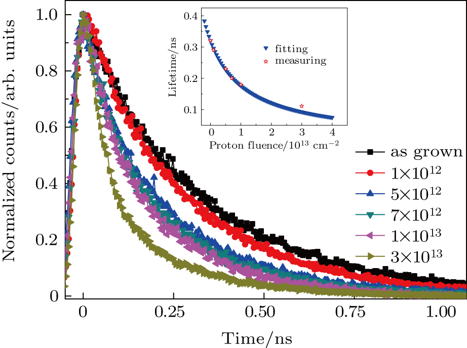
To gain a physical insight into the radiation effect on nanowires (NWs), the time resolved photoluminescence (TRPL) technique is used to investigate the carrier dynamic behaviors in GaAs/AlGaAs core–shell NWs before and after 1-MeV proton irradiation with fluences ranging from 


Recently, due to the excitation of unique electronic and optical properties of these nanostructure, GaAs/AlGaAs core/shell NWs have been studied in a broad range of optoelectronic devices such as light-emitting diodes,[1] laser diodes,[2,3] solar cells,[4,5] and photodetectors[6,7] working towards the energy conservation and environment protection. One important point is that as an alternative material to silicon, GaAs offers the possibility of higher radiation resistance[8] and a better overall performance.[9] However, despite these advances, there is still an uncertainty over the role of point defects and/or defect clusters that may be present at exceedingly high density, which could destroy semiconductor devices in the radiation environment, such as space and atom energy field. The materials used in the relevant units above must withstand long-term use in strong radiation fields. It is well known that nano-material and nano-devices, such as quantum dot[10] and quantum well,[11] present radiation hardness intrinsically.[12–15] Although the proton irradiation-induced intermixing effect in GaAs-AlGAs quantum well has been investigated[16–18] and ultra-thin GaAs solar cell with intrinsic radiation tolerance has been demonstrated,[19] these results have not been comprehensively explained due to the lack of systemized theory and data study. In terms of ion irradiation on NWs, currently the research mainly focuses on the doping profile of NWs,[20,21] or bending and alignment for shaping NWs.[21,22] Therefore, it is significant to develop the radiation effect theory and conduct experiments on NWs to understand the radiation effect on NWs in this corresponding area.
There are two categories of defects created by radiation, and they have distinctively different characteristics.[23] The first category, called point defects, includes at most a few atoms aggregated together to form a relatively stable and simple defect. The second category, called a defect cluster, involves a few hundred atoms in a large disordered region. A displacement damage effect occurs when displacement defects are created in the crystal lattice, thereby introducing additional states in the forbidden band. This displacement damage to optoelectronics devices in the Van Allen belt by electrons and protons tends to be of the simple defect variety.[23] Apparently in this case, the transmission electron microscope (TEM) technique is unable to provide enough resolution to directly observe the point defect in the crystal. Other techniques such as temperature-dependent Hall-effect (TDH), deep-level transient spectroscopy (DLTS), positron annihilation spectroscopy (PAS), and photoluminescence (PL) spectroscopy, have been employed to characterize single crystal and their defect states. While the first three techniques are used for studying materials from different viewpoints, they are the known well-established tool for bulk solids and thin films.[24,25] These methods show several limitations and technical challenges, because of the formation of Ohmic contact for instance. Besides, the displacement lattice damage in semiconductor material can have a significant influence on their electrical or optoelectronic properties, through creating more than one deep-level defect in the bandgap. Consequently, the important material parameters such as free carrier mobility and density, resistivity and generation and recombination lifetime will be affected by displacement damage. The relevant study on single NW is likely to be an extreme challenge, such as the stability of fabricating a single NW device. On the other hand, micro-photoluminescence spectroscopy (μ-PL) could largely overcome these difficulties. In addition, it can be applied to the case where there is a low defect concentration in single NW, provided that competitive non-radiative carrier recombination is not the overwhelming optical transition. Our previous study has demonstrated that the NWs with smaller diameter, which has a relatively high surface-to-volume ratio, could have greater radiation tolerance.[26] This work highlights the potential of the photoluminescence technique to estimate the irradiation-induced defect concentration by measuring minority carrier lifetime of NWs.
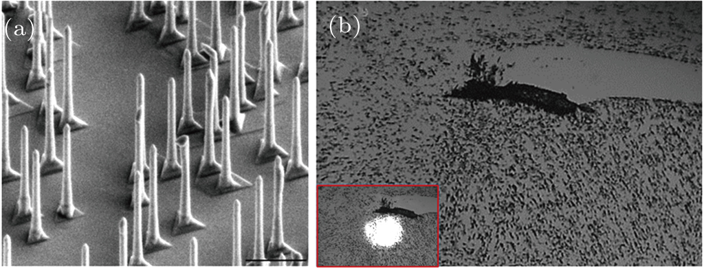
All the samples and equipment used in this study were provided by the Semiconductor Optoelectronics and Nanotechnology Group at the Department of Electronic Material Engineering, Australian National University. The GaAs/AlGaAs core-shell NWs grown via the metal-seeded vapor–liquid–solid (VLS) growth method in a metal–organic vapor phase epitaxy (MOVPE) system. The growth of the NWs, structural characterization, and PL characterization methods have been described in earlier publications by Joyce et al.
[27–29] Trimethylgallium (TMGa), trimethylaluminum (TMAl), and arsine were used as the precursors for Ga, Al, and As, respectively. Gold particle size ∼ 50 nm was used and GaAs core NWs were grown using the two-temperature procedure.[30] An AlGaAs shell was then grown around the GaAs core at 750 °C with an Al mole fraction of 0.5 (ratio of TMAl/(TMAl+TMGa)


All the samples were irradiated by using 1-MeV H


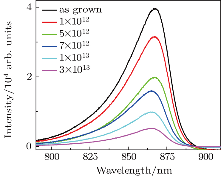
The plots of the PL intensity as a function of wavelength at different irradiation fluences for a typical cluster of GaAs/AlGaAs core/shell NWs are shown in Fig. 


Considering the fact that the minority carrier lifetime 


Then the corresponding carrier lifetime damage coefficient 


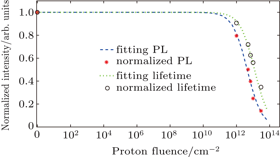
To directly see the reduction of minority carrier lifetime and degradation of the PL intensity versus radiation fluence, here we define the normalized carrier lifetime as


Under low level injection conditions, the dependence of PL intensity on external injection and minority lifetime in NWs can be expressed as:[26]


Carrier lifetime is extremely important from a device-physics standpoint, because it governs the operation of semiconductor p–n junctions, one of the basic device structures, to a large extent.[32] In contrast to the bulk recombination lifetime, surface recombination is more sensitive to ionization damage, and only marginally to displacements.[32] Studies have also found that the AlGaAs shell acts as a passivation layer which could eliminate the surface states for GaAs NWs core.[29,38] One important point, however, is that the surface recombination is determined by the density of interface traps and the surface potential. Hence this study takes it into account that the surface recombination remains constant after irradiation. On the other hand, Shockley–Read–Hall (SRH) recombination mechanism is typically used to discuss the recombination of electron-hole pairs at defect levels within the bandgap.[39] It has been usually described in the frame of the SRH theory,[37] in which the thermal (i.e., phonon-assisted) carrier transitions to and from the bands are considered. In principle, it can be extended to taking into account the contribution of different recombination centers, radiative lifetime, and the surface recombination lifetime. Hence, there is more than one deep-level defect present, and the total SRH lifetime of the NW at the low-injection level can be described by 


In summary, the radiation effect on GaAs/AlGaAs core-shell NWs with core diameter ∼ 50 nm is studied by proton irradiation in combination with the PL measurement technique. The model of relation between PL intensity degradation and minority carrier lifetime decline is obtained and explained under low photon injection and low proton irradiation fluence. Furthermore, the radiation effects on surface recombination and radiative recombination could be eliminated in the GaAs/AlGaAs core-shell NWs, and the irradiation-induced defect concentration can be extracted from the measurement of minority carrier lifetime. The results and their understanding achieved from this work will help further investigate irradiation-induced defects in nano-materials for space or atomic energy applications.
| [1] | |
| [2] | |
| [3] | |
| [4] | |
| [5] | |
| [6] | |
| [7] | |
| [8] | |
| [9] | |
| [10] | |
| [11] | |
| [12] | |
| [13] | |
| [14] | |
| [15] | |
| [16] | |
| [17] | |
| [18] | |
| [19] | |
| [20] | |
| [21] | |
| [22] | |
| [23] | |
| [24] | |
| [25] | |
| [26] | |
| [27] | |
| [28] | |
| [29] | |
| [30] | |
| [31] | |
| [32] | |
| [33] | |
| [34] | |
| [35] | |
| [36] | |
| [37] | |
| [38] | |
| [39] | |
| [40] | |
| [41] | |
| [42] |


