† Corresponding author. E-mail:
The thermal stability of a vertical-cavity surface-emitting laser (VCSEL) array is enhanced by redesigning the mesa arrangement. Based on a thermoelectric coupling three-dimensional (3D) finite-element model, an optimized VCSEL array is designed. The effects of this optimization are studied experimentally. Power density characteristics of VCSEL arrays with different mesa configuration are obtained under different thermal stress in which the optimized device shows improved performance. Optimized device also shows better stability from measured spectra and calculated thermal resistances. The experimental results prove that our simulation model and optimization is instructive for VCSEL array design.
Vertical-cavity surface-emitting laser (VCSEL) offers some natural advantages over edge-emitting laser (EEL) like symmetrical laser beam and simple arrangement in two dimensional (2D) arrays, and are very attractive laser sources for a wide range of applications in optical interconnect, parallel links, free space communications, laser pumping, illumination,[1–6] gesture recognition and 3D sensing.[7,8] These applications all demand the device’s reliability, which largely depends on the thermal stability. For example, operating lifetime of the VCSEL decreases exponentially with temperature rising, and excessive temperature rise in the active region can reduce the VCSEL array’s reliability drastically.
Thus, it is important to investigate the thermal issue of the VCSEL and many researchers have made great efforts on it. Nakwaski et al.[9] analyzed the current flow and temperature rise in etched-well VCSEL using the electrical analog method; Chen et al.[10] developed an effective electrical conductivity model and considered size effects on the electrical, thermo-physical, and radiative properties; Choi et al.[11] studied the thermal effects of 850-nm VCSEL using thermal-electric direct-coupled field analysis. These works provided valuable references both theoretically and experimentally, and usually focused on single VCSEL. Meanwhile it is common for many applications to take full advantage of the VCSEL array, so efforts have also been made for thermal characteristics of the VCSEL array. Wang et al.[12] investigated the effects of oxide-aperture and substrate thickness. Holger Moench et al.[13] simulated the heat flow in VCSEL array and presented an elongated rectangle shaped VCSEL array to achieve higher power. However, those studies basically focused on thermal characteristics of the single VCSEL device or the whole array device. Researches aiming at improving thermal stability of the VCSEL array by designing a mesa arrangement according to the heat coupling among mesas are lacking. The mesa arrangement is of great potential to have strong effects on the interplay of heat flux among different mesas in the VCSEL array, without alteration of the wafer structure and extra fabrication process. The interaction of heat flux among mesas will finally affect the temperature distribution and consequently the whole device performance.
In this paper we put forward a specially designed VCSEL array with non-regular mesa arrangement in order to enhance the thermal stability and reach higher power without overlarge mesa area. A 3D thermoelectric coupling analysis is performed to compare the temperature distribution inside the VCSEL array with different configuration of mesas. Based on the analytical results, we redesign the arrangement of mesas in order to lower down the heat coupling among mesas. Then, effects of the optimization(redesigning) were investigated experimentally. Light-current (LI) performances under different heat sink temperatures of the optimized array were compared to devices with normal 4×4 square arrays. Furthermore, we studied the spectra and central wavelength shift of arrays with different mesa arrangement, from which the thermal resistances were calculated. At last, far field patterns of different devices were measured.
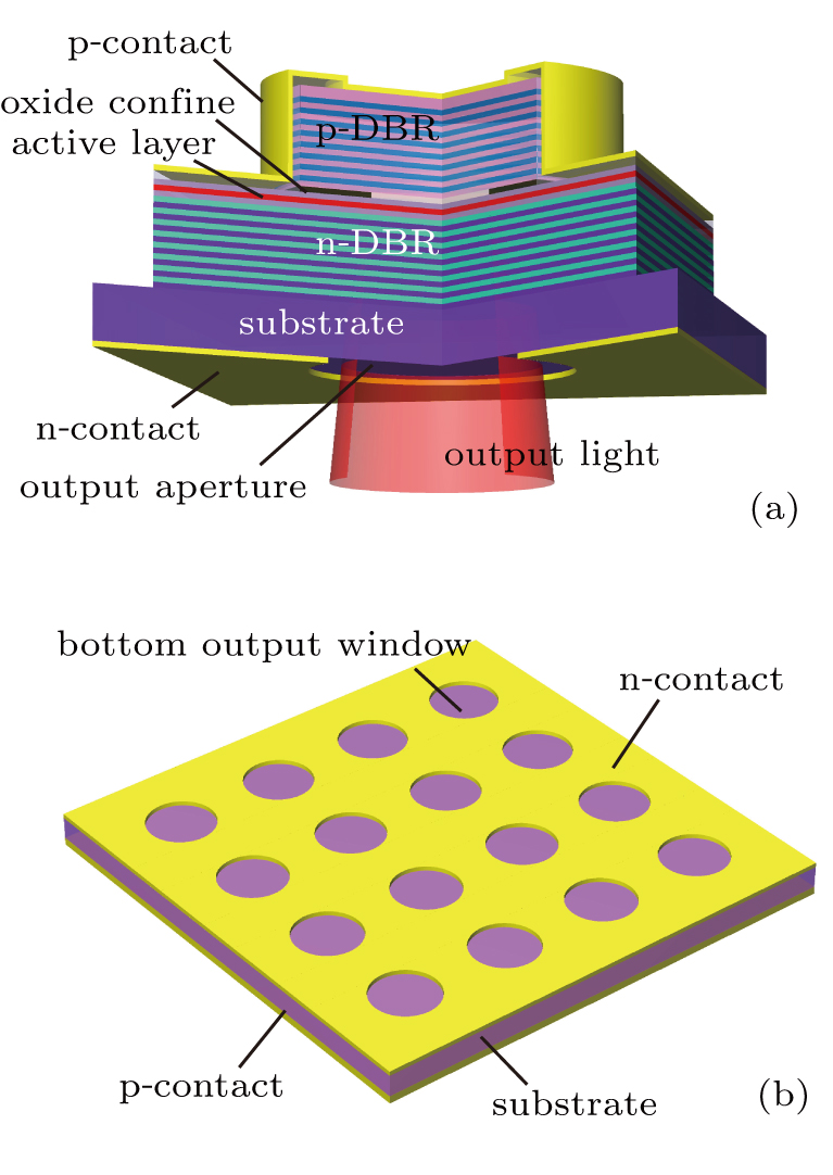
The scheme of a single 980-nm bottom-emitting VCSEL device and the array are shown in Fig.
Circular mesas are etched on the p-doped side of the wafer by chlorine using inductively coupled plasma (ICP) equipment. After a selective oxidation process, SiO2 is deposited on the surface of the mesas using plasma enhanced chemical vapor deposition (PECVD). Then the SiO2 on the top of the mesas is etched away by fluorine using ICP equipment and the p-contact is formed by DC sputtered Ti/Pt/Au. The GaAs substrate is then reduced down and polished. After sputtering of Ge/Au/Ni/Au, the output window is made by the lift-off process and the antireflection layer is grown on part of the wafer to avoid back reflections into the cavity. Finally the wafer is split apart, bonded to a C-Mount heat sink and packaged into TO-3. Further details of the device structure and output characteristics are published in Ref. [14].
To quantify the temperature distribution, heat source distributions in the VCSEL must be determined. In the DBR and the substrate layers, thermal resistance is the main heat source. In the active region, heat mainly comes from non-radiative recombination and resistive heating.[15]
Under steady state conditions, the electrical potential in the VCSEL is determined by the Laplace equation:
 |
To consider the interface and boundary scattering effects of phonons and electrons,[16,17] anisotropic material properties are used in the active layer and DBR region. The electrical conductivity σ in Eq. (
 |


 |


 |


 |
 |
We had considered the temperature-caused variation of thermal conductivity[19]
 |
Finally, the Joule heating 


 |
Table
| Table 1.
Material properties used in the simulation. . |
The primary purpose of our simulation is to investigate the temperature variation tendency of arrays with different mesa edge distances. Therefore, specifically, device structure in our simulation was simplified. The oxide layer is thin enough to be omitted and the oxidized part is regarded to be adiabatic, so the mesa’s diameter was the same as the oxide aperture’s being 100 μm. Thus we only constructed four main heat sources of a VCSEL: p-DBR, active layer, n-DBR and the substrate, which are sufficient enough to explore the thermal influence of different mesa arrangements.
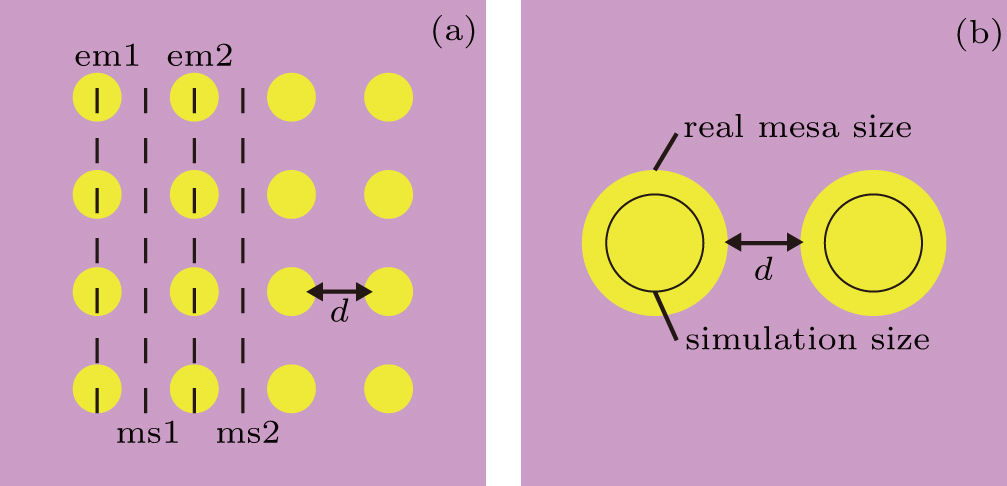
As shown in Fig.
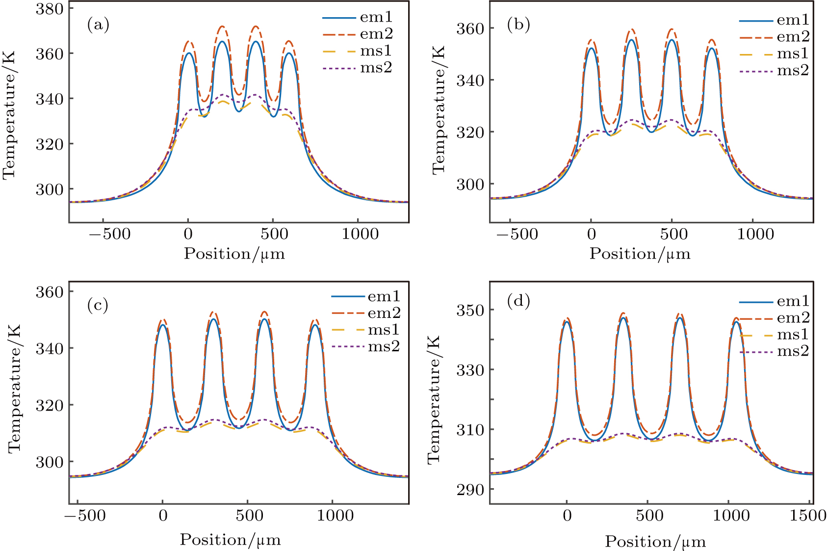
The surface temperature distribution and details on the active layer plane when adding 3-A current were obtained. Figure
Figure
To have a closer insight, we investigated 20 mesa edge distances varying from 50 μm to 350 μm as shown in Fig.
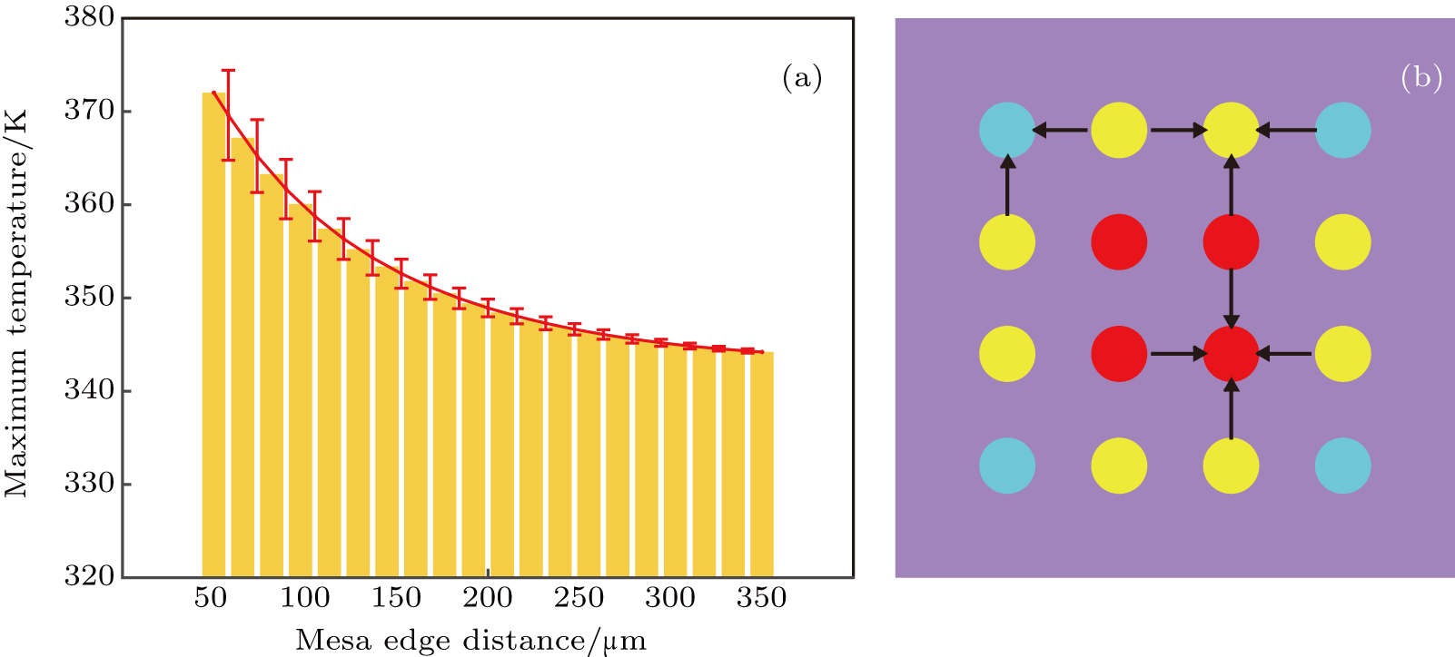 | Fig. 5. (color online) (a) Maximum temperature for VCSEL arrays with different mesa edge distances ranging from 50 μm to 350 μm and (b) illustrative interaction among mesas. |
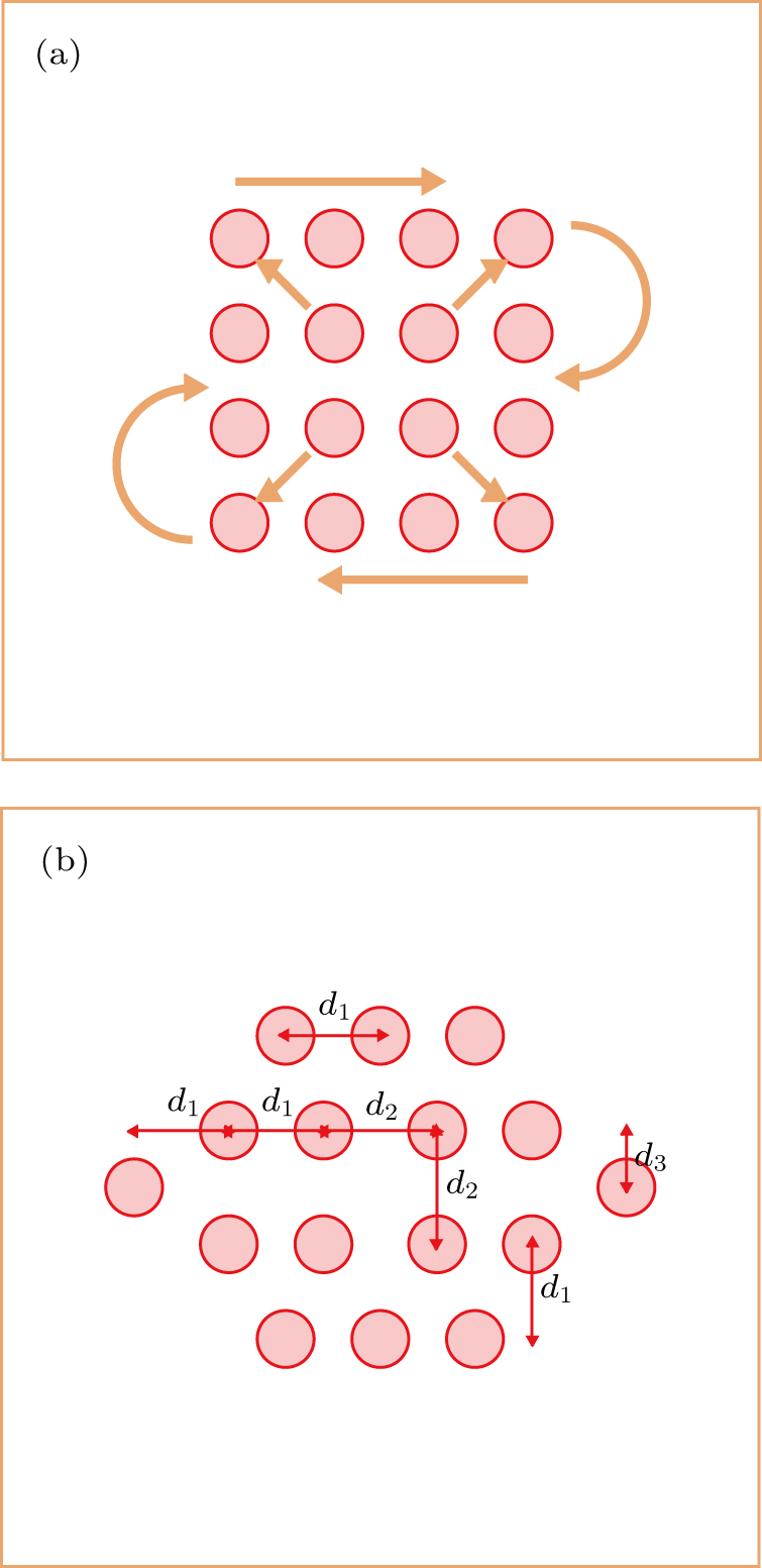
Simulation results above indicate that the mesa distance together with the number of mesas surrounding have the main influence on thermal interaction among mesas. We give our explanation by sorting mesas into three types: the corner type, edge type and central type, marked sky-blue, yellow and red color respectively as depicted in Fig.
According to the simulation, mesa distance has proven to have non-negligible influence on thermal characteristics of the device. Larger mesa distance can help avoid more heat coupling. However, the result in Fig.
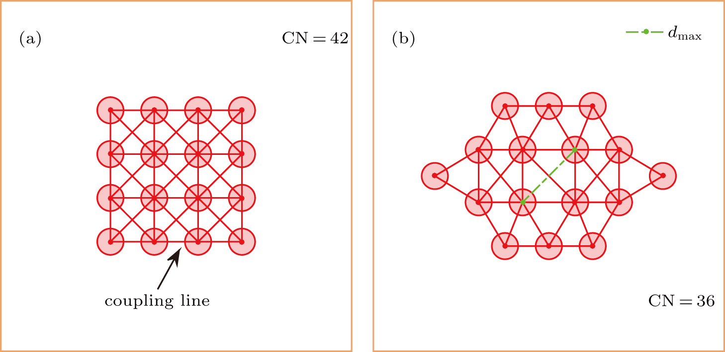
The priority in our optimizing process is to reduce the heat coupling among meas as much as possible and then comes the whole mesa area. We chose the normal 4×4 mesa arrangement as the initial arrangement. Compared to the normal device, the distances of mesas in the central part got larger in the optimized array, because heat coupling among them is more serious than other mesas’.
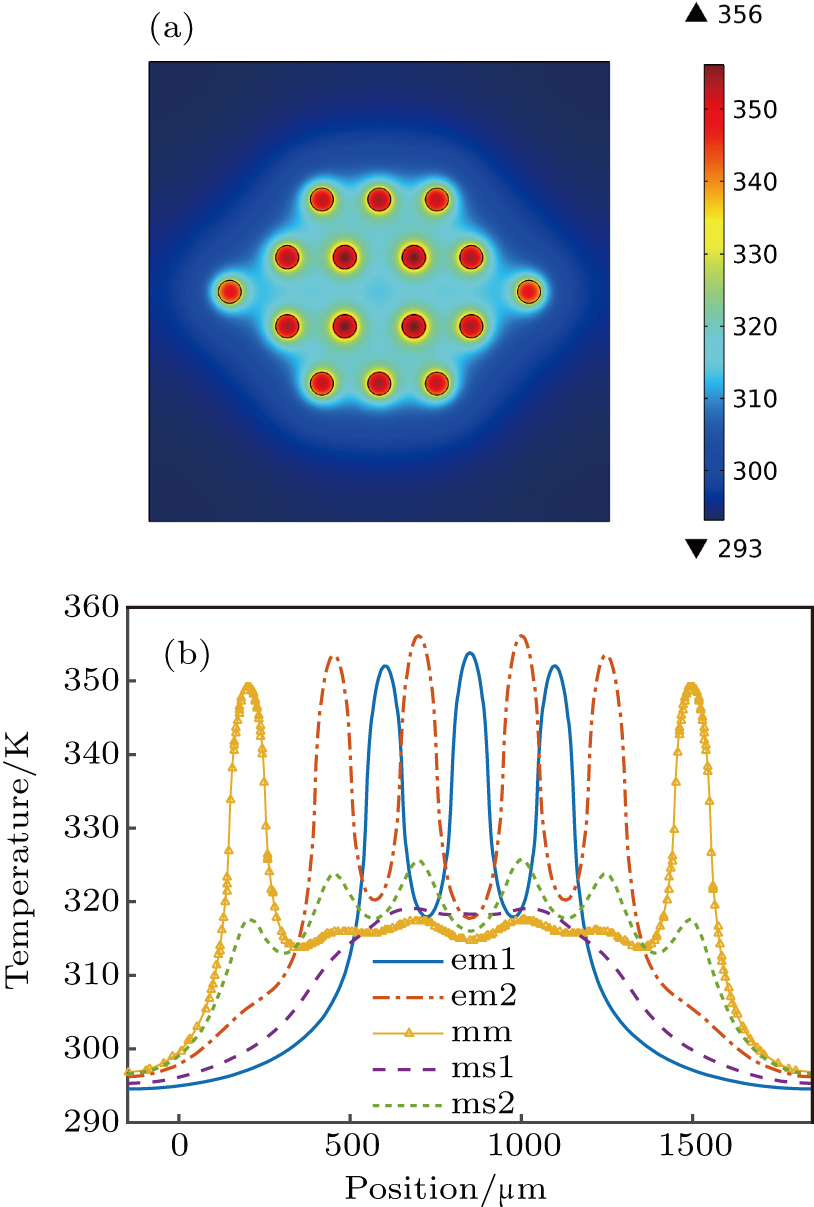
Also, the position of some mesas were modified. Two mesas at the corners were moved to the centers of left and right sides respectively. Three remaining mesas on the top and bottom sides were moved to the center in their original rows. The existence of interaction between mesas is visualized in Fig. 
Using exactly the same material parameters, boundary conditions and driving current of the 4×4 square mesa arrangement VCSEL array, we performed a simulation for the optimized one using COMSOL Multiphysics® again. Through the surface temperature distribution and details on the active layer in Fig.
According to the simulation, we fabricated three kinds of VCSEL arrays with different mesa arrangement. 4×4 square array with mesa edge distances being 100 μm, 150 μm and the optimized array were fabricated as a bottom emitting VCSEL array on the same wafer with the same mesa diameter of 150 μm. The optimized array has an irregular distribution of mesa, but it requires no additional fabrication process except changes of lithography mask.
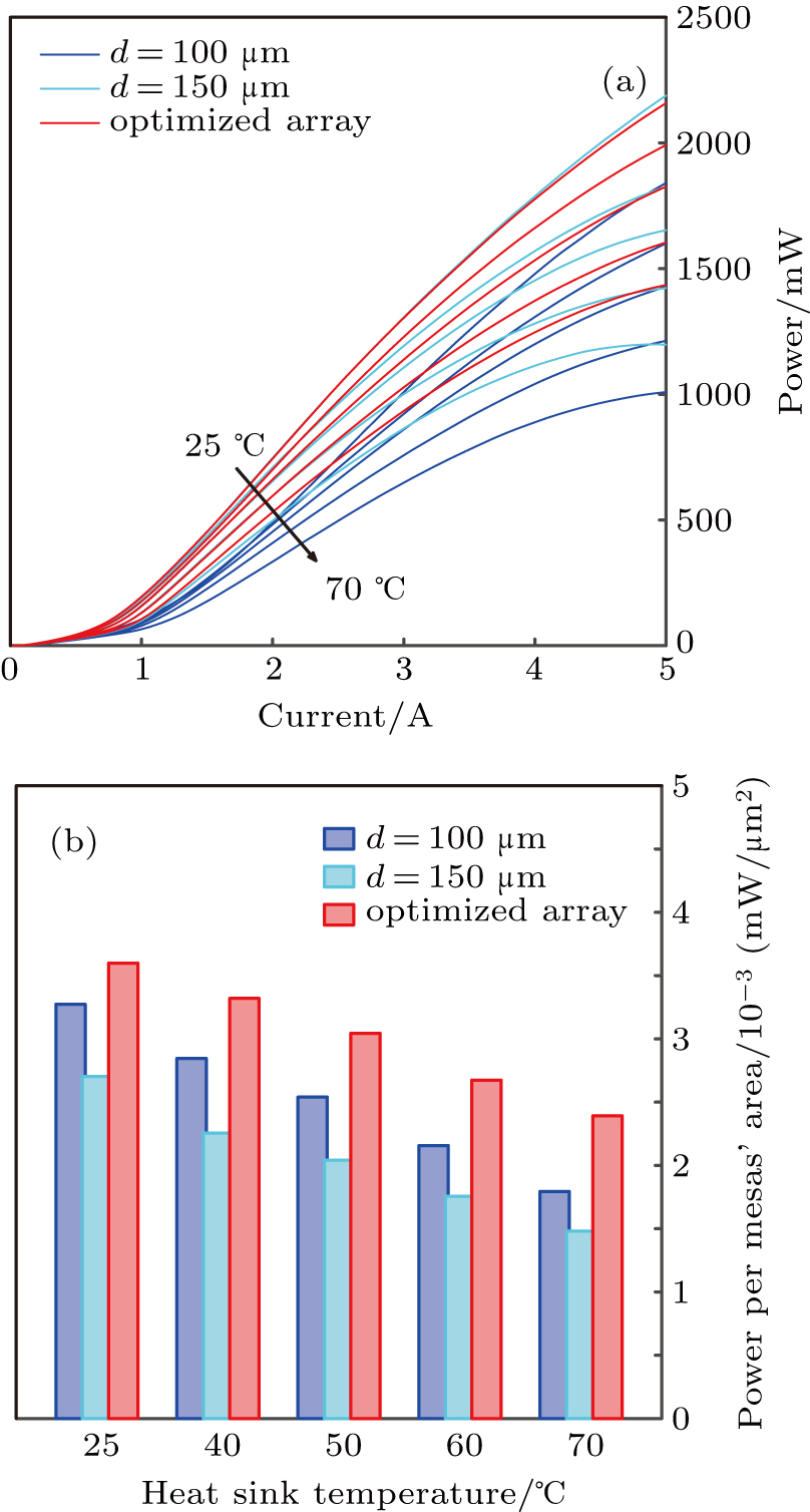
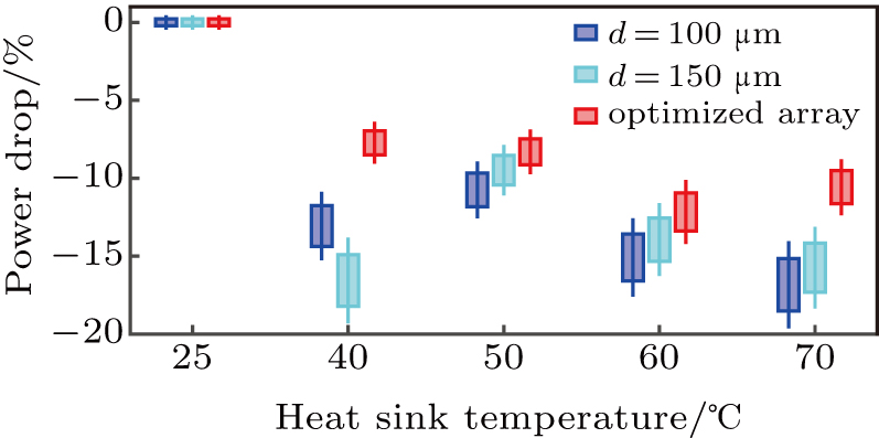
LI characteristics in different heat sink temperatures were tested under the CW condition. Due to the limit of maximum current (5 A), our device testing equipment could not make the devices reach the thermal roll-over point. It could be seen from both the LI curves for different temperatures and the statistical histogram of maximum power per mesas’ area (the maximum power divided by the mesas’ distribution area) in Fig.
The bottom emitting VCSEL device is sort of a flip chip as its p side is mounted on the heat sink. Hence the outer heat was transferred directly from p-DBR to the active layer, the case in which diffusing the heat among mesas away as much as possible becomes so important. Since each single mesa has the same epitaxial structure, factors relevant to the macro-structure like mesa arrangement is the key to lowering the thermal interaction among mesas. Figure
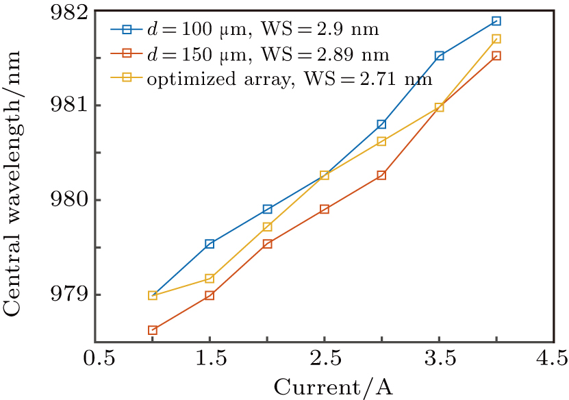
To further investigate the thermal stability of different types of devices, spectra and wavelength shift were tested. Working on a copper heat sink without heating and water-cooling, the central wavelength shift for different devices varied as illustrated in Fig.
 |
The measured wavelength-temperature variation (
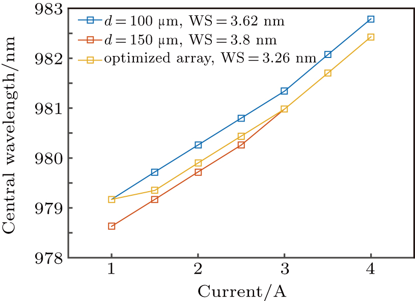 | Fig. 11. (color online) Central wavelength shift (WS) for different VCSEL array with heat sink at room temperature. |
For this condition, we can also calculate the thermal resistance defined as
 |


| Table 2.
Thermal resistance(K/W) of different devices. . |
When adding water cooling, self-generated heat from the VCSEL array was constantly transferred to the heat sink, the central wavelength shift got shrunk as shown in Fig.
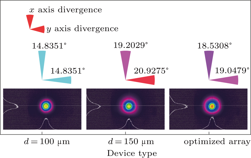
Far field patterns of different devices at 3.5 A were measured as illustrated in Fig.
A 3D thermal-electrical coupled finite-element method was developed to investigate the thermal characteristics of a 980nm high power bottom emitting VCSEL array. The simulations showed that a different mesa arrangement had an effect on the heat coupling between mesas. Optimization of the mesa arrangement was performed in order to improve the thermal behavior of the VCSEL array device. In the experimental investigation of VCSEL arrays with three kinds of mesa arrangements, the optimized VCSEL array has shown obvious advantages on LI characteristics and its thermal stability excels according to the spectra and thermal resistance under different driving currents. The optimized array has an average reduction of 1.2312 K/W in thermal resistance compared to normal VCSEL arrays at different current scales. Besides, it can reach higher output power while maintaining a not oversized mesas’ area and far field patterns suggest that non-central symmetry will not bring a negative effect to the device. The arrangement of VCSEL mesa has been proven to have a positive influence on device performances. It can be concluded that our optimizing process has efficiently reduced the thermal interplay between mesas and is instructive to array design. Finally, our optimizing method is after all a qualitative one and promisingly can be improved to a more perfect, quantitative one.
| [1] | |
| [2] | |
| [3] | |
| [4] | |
| [5] | |
| [6] | |
| [7] | |
| [8] | |
| [9] | |
| [10] | |
| [11] | |
| [12] | |
| [13] | |
| [14] | |
| [15] | |
| [16] | |
| [17] | |
| [18] | |
| [19] | |
| [20] |


