1. IntroductionAs the integrated circuit is used more and more widely in civil and military fields, research on microelectronic reliability has been a hotspot in recent years. The failures caused on the semiconductor could be various, such as a material defect, device aging and radical external excitation. High power microwave is a typical instance of electromagnetic interference with a high power level, high frequency and short width generally, and is developed rapidly for the use of microwave weapons. High power microwave (HPM) is easy to couple into electronic system via antennas, cables and apertures of shells intentionally or unintentionally, leading to degeneration in performance and temporary or permanent failure.[1]
Since the external microwave may induce a catastrophic impact, the microwave effects on various integrated circuits and semiconductors have widely been investigated in these last few years. Many experimental researches were carried out through testing the damage susceptibility of discrete PIN diode,[2] high electron mobility transistor (HEMT),[3,4] bipolar transistor,[5] integrated components on transistor–transistor logic (TTL) and CMOS logic,[6] computer system,[7] etc. Besides, theoretical studies were also presented widely. Ren et al. reported the motion of current filaments and the thermal failure effect of PIN diode under electromagnetic pulse.[8] Liu et al.[9,10] and Yu et al.[11,12] revealed the phenomena of damage and degradation as well as their mechanisms of GaAs HEMT under the influence of HPM by numerical simulation and experiment used for comparison. Chai et al.[13] and Ma et al.[14–16] proposed the thermal failure mechanism in bipolar semiconductor and proposed some measures against it. As for the CMOS device, Kim and Iliadis focused on the dynamic and static characteristics in a CMOS inverter under HPM environment.[17–20] Wang et al.[21] and Yu et al.[22–24] researched the HPM induced latch-up effect and its critical factors in experiment and theory. However, the thermal damage is also a significant failure cause for the CMOS device besides latch-up.[1]
This work focuses on the thermal failure in the CMOS inverter caused by HPM. An analytical temperature distribution is derived and the relationships between hotspot temperature and microwave frequency, and between hotspot temperature and width are predicted. Based on numerical simulation, the damage mechanism is presented and the temperature model is validated and explained. In addition, the variations of damage threshold with frequency and width are predicted and compared with simulation results and reported data.
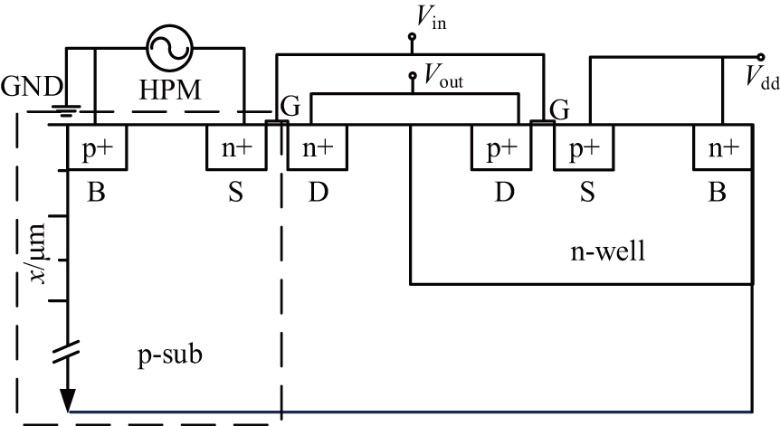
2. Modeling procedureA typical CMOS inverter schematic diagram with an n-well is depicted in Fig. 1. The doping types and the electrical connections are illustrated, and B, S, D, G represent bulk terminals, source terminals, drain terminals, and gate terminals of NMOS or PMOS, respectively. The top surface is regarded as being adiabatic and the lower surface is assumed to be at ambient temperature (300 K). For digital circuits, the external microwave is more likely to invade the electronic system via a back-door couple path,[1] of which power/ground lines are typical instances, thus the external HPM injection source acts on the source terminal of the NMOS part in our work. The external HPM is assumed to be a sinusoidal plane wave, which has been proved to be equivalent to actual HPM coupled with wires approximately.[25]
Obviously, during the positive semi-period of the external microwave, the PN junction across the bulk and source terminal becomes biased reversely, and there is only reverse current which can be ignored since an avalanche effect has not been taken into consideration. However, when the external electric potential turns negative, current paths from the bulk and source terminal near the device surface occur, leading to a Joule heat production. In this case, the temperature of this region will rise up if the heat cooling rate is less than the heat generation rate. Thus, the surface temperature presents a periodic “down-up-down” variation, and the device maybe burns out at the hotspot finally.
According to the above analysis, the rise in device temperature is due to the forward current across the “N
 –P–P
–P–P
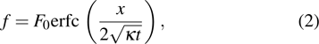
 ” structure between the source and the substrate terminal during the negative semi-period of external microwave, and the hotspot is close to the top surface of the device. Therefore, it is reasonable to regard the device (NMOS side) as a one-dimensional (1D) semi-infinity vertical solid medium with the origin point located at the top surface as seen in Fig. 1 and marked by the dash line. Here, we first regard the heat induced by the forward current resulting from external HPM as a constant flux heat at x = 0. Hence, the heat flux f inside the device satisfies the following equation with a Dirichlet boundary condition:[26]
where
x is the vertical position,
t is the time,

is the equivalent boundary flux heat and

is the thermal diffusivity which is actually relevant to temperature. For simplicity, the thermal diffusivity is assumed to be a constant in our work. The solution of Eq. (
1) can be expressed as follows:
[26]
where erfc(
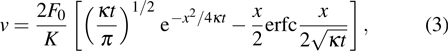
x) represents the complementary error function. The temperature distribution
v along the
x axis, which is the integral form of heat flux, can be obtained as
[26]
where
K is the thermal conductivity which is proportional to thermal diffusivity {

}, and assumed to be a constant as well. However, the surface heat fluxes are periodic, which are not identical during different temperature-rise processes. During the positive semi-period of the microwave, the heat flux can be considered as zero since there is no heat production according to the previous discussion, and the border is adiabatic, whereas during the negative half of the
N-th period, the heat flux is defined as

. Obviously,

represents the equivalent heat flux during the 1st cycle of microwave now. Therefore, after
N periods of microwaves, the temperature can be obtained according to the superposition principle as follows:
where
T is the period length of microwave,

is the initial temperature of device (300 K), and
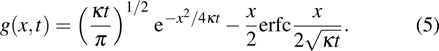
g(
x,
t) represents the following relationship:
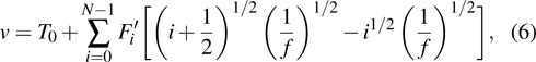
According to our previous discussion, the hotspot exists at the surface of the device, hence the max temperature is located at x = 0, and equation (4) where x = 0, can be expressed as follows:
where

is a simplified value calculated by

and
K,
f is the HPM frequency, and
N is the total number of microwave periods, which is equal to
f multiplied by pulse width

. The

reflects the heat flux of the surface during the negative semi-period of the (
i-1)th microwave period, and it is proportional to the forward current across the junction. On the other hand, the PN forward junction has a power-law relationship with temperature, that is to say,

has a power law with the following expression:
Therefore, equation (6) reveals a complex relationship between v and f, and an equivalent heat flux level
 is adopted in our work, which reflects the average flux level of
 throughout the duration of
 . According to Eq. (7),
 can be considered as a power function of f and
 . Hence, the max temperature inside the device under an injected microwave with a frequency f and pulse width
 is obtained as follows:
One thing should be noted, i.e., the injection power level is assumed to be a constant value in the above discussion, whereas it contributes to
 positively actually, and the fitting coefficients are related to the injection power.
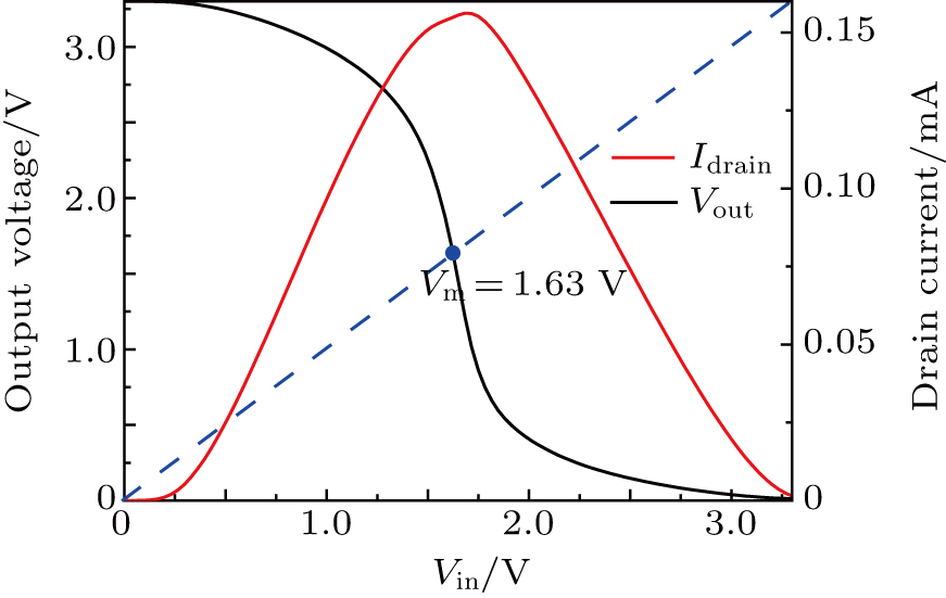
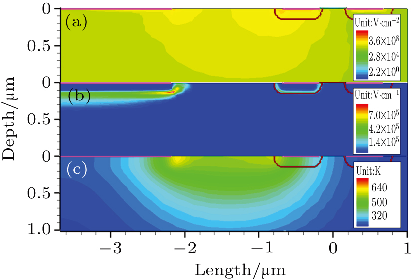
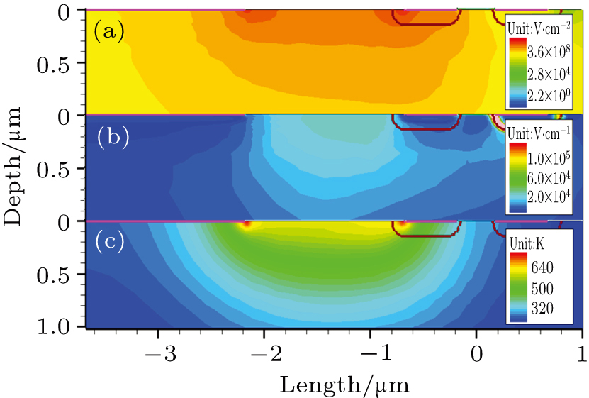
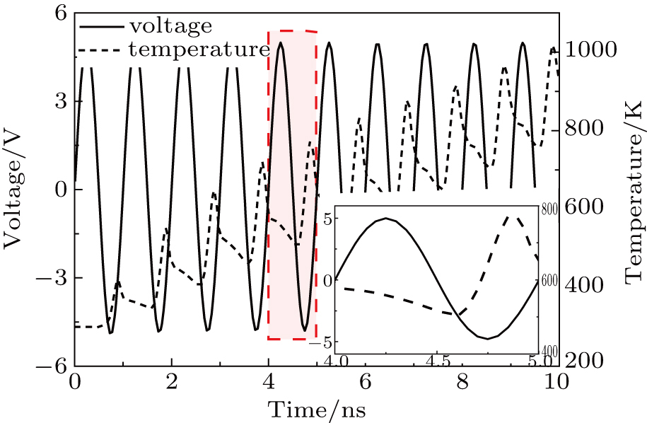
4. Results and discussion4.1. Process of temperature variationThe maximum temperature inside the CMOS inverter responding to the injected microwave with a peak induced voltage of 5 V is shown in Fig. 3. The temperature curve presents a periodic “rise-fall” trend, which is consistent with the analysis in Section 2. However, the max temperature turns higher overall, and it should reach the melting point of silicon finally, leading to a partial short-circuit and invalidating the function of the device. In order to study the details of the temperature-rise process, the part of curves (from 4
 ns to 5
 ns) are zoomed in. The result is consistent with the analysis in Section 2, in which it can be seen that the temperature rises during the negative semi-period and it decreases during the positive semi-period. Since the variation in temperature results from Joule heat, and the rate of power depends on electric field strength and current density: these physical quantities of the NMOS side are extracted from Figs. 4 and 5.
Obviously, when the external electric potential is positive, the junctions of N
 –P and P–P
 are biased reversely, and the electric fields concentrate on depletion layers. The external voltage is divided by two junctions, and the impact ionization is not enough to trigger an avalanche effect, hence there is little current from the source to the bulk terminal. The heat flows towards the substrate, and the temperature decreases. However, when the external electric potential is negative, an apparent forward-current path forms. Since the current density is quite large, it tends to form hotspots at the junction region, where the radius of curvature of the electric field is small. Therefore, if the rate of heat generation is higher than the cooling rate, the temperature becomes higher.
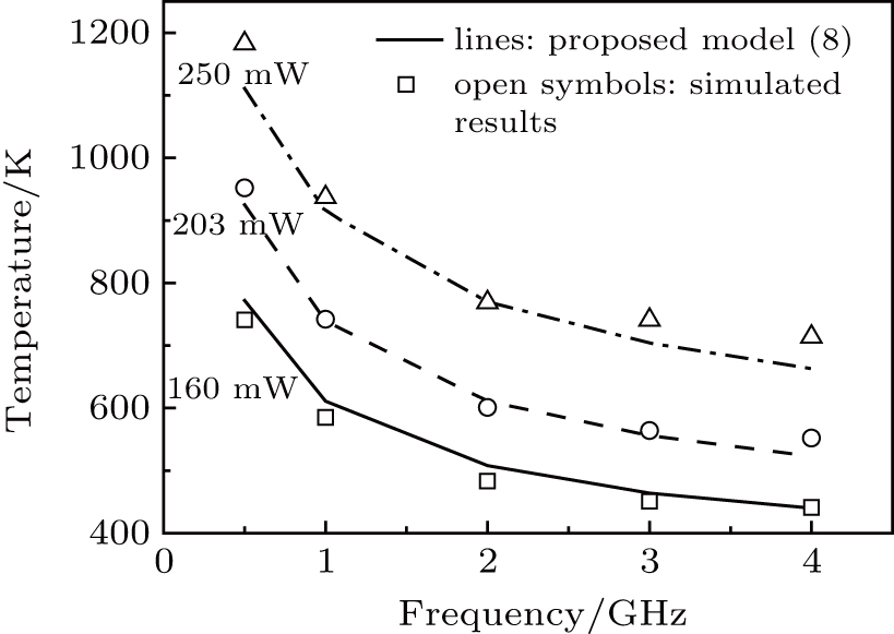
4.2. Validation of the maximum temperature modelEquation (8) reveals the relationship among maximum temperature of the device and pulse width and microwave frequency. In order to verify the validity of this model, the simulated max temperatures versus microwave frequency under diverse injection power levels are shown in Fig. 6. The pulse width is specified as 10 ns, and it is seen that the max temperatures decline with frequency increasing from 0.5 GHz to 4 GHz. The analytical model (8) is used for fitting this relationship and the results are also exhibited in Fig. 6. The fitting curves show the same trends as the curve of simulated data, proving the validity of the frequency effect.
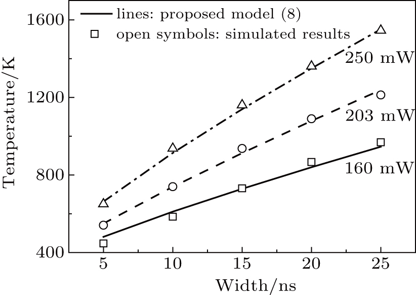
Besides, the relationship between max temperature and microwave pulse width is obtained by simulation and shown in Fig. 7. The results show a positive correlation between pulse width and max temperature. It is reasonable since the temperature increases continuously under the effect of the injected microwave with a constant frequency and power level. The analytical model (8) is also presented in Fig. 7 and shows the same trend as simulated data, validating our analysis above.
4.3. Dependence of
 on pulse width and frequency
As mentioned in Section 2, an equivalent heat flux
 is adopted to represent the average heat flux in
 duration, and it is reasonable to consider
 as a power function of f and
 . In our work,
 is approximated as follows:
where

and

are calculated to be negative values and positive values, respectively, and

is the value related to injected power positively. The signs of

and

reveal that the average heat generation rate is actually negatively related to microwave frequency and positively related to pulse width. According to the previous analysis, the heat generation behavior results from PN forward current, and the forward current is related to temperature positively. Since the peak temperature increases overall with time going by, the heat generation rate increases, that is to say,

is an increasing function of
i. So it is deduced that for a certain frequency and power level,

is an increasing function of microwave pulse width

.
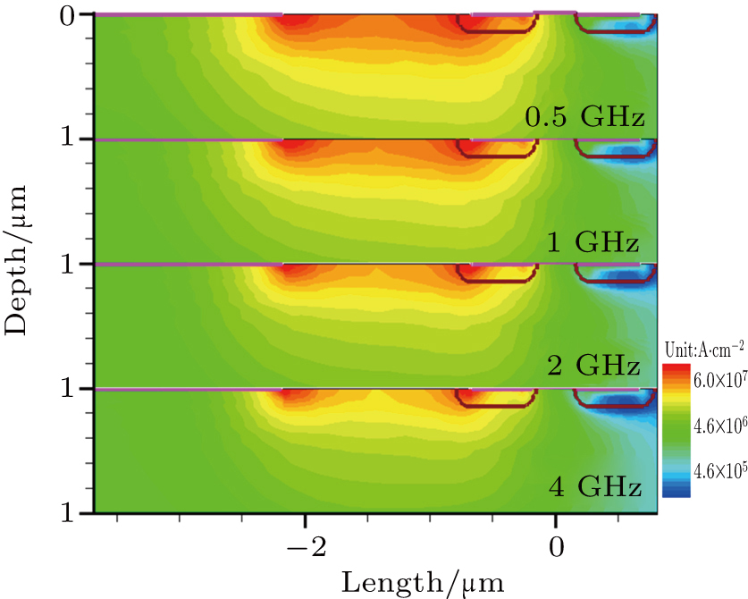
Furthermore, for a microwave with a lower frequency, the duration of each cycle is longer, and the temperature of the hotspot is larger after a temperature-rise period, leading to a larger junction current for the next cycle in turn. After the same period of time, the temperature and the current density are both higher for lower frequency, resulting in a larger
 . The scenario which can be considered as positive feedback is illustrated in Fig. 8, where the current densities at microwave negative semi-period of diverse frequencies after the same period of time are shown. It is apparent that the forward current density varies with frequency reversely; therefore,
 can be seen as a negative function of f, as we calculated previously.
4.4. Dependence of damage threshold on pulse width and frequencyAs we mentioned in Section 2, the maximum temperature inside the device presents a periodic variation and increases overall, and it is proved that the burn-out point is located at the top surface. For a microwave with frequency and pulse width fixed, one can obtain a relationship between equivalent heat flux
 and max temperature. Noticing that the forward current is apparently related to the induced voltage,
 is an increasing function of induced voltage or injected power level. In Eq. (8), it is easy to prove the summation term
 to be an increasing function of
 , and a decreasing function of f. Hence, a larger
 is needed for microwave with higher frequency and shorter pulse width to reach the silicon melt point
 . However, f and
 contribute to
 oppositely for a certain injection power level (i.e.,
 actually becomes smaller with increasing f or decreasing
 if injected power is a constant), where the trends are the same in the summation term {
 }, according to the signs of
 and
and
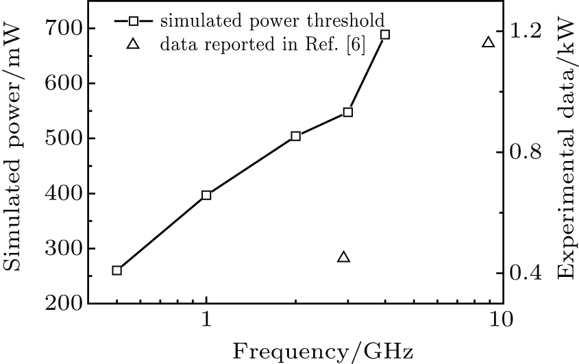
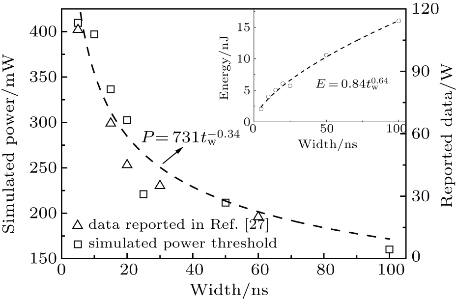
 in Eq. (9). That is to say, the device damage power threshold increases with a higher frequency and a shorter pulse width. The derived conclusion is consistent with the simulation data as seen in Figs. 9 and 10. In Ref. [6] some typical CMOS integrated components were tested under diverse frequencies, and in Ref. [27] the pulse width effect of PN junction damage was investigated. The reported data are also shown in Figs. 9 and 10, which are in accordance with the conclusions in this work, and the simulated pulse width dependence satisfies the Wunsch–Bell relationship.[28] In addition, the damage energy thresholds are also calculated and given in Fig. 10, showing an increase for a longer microwave generally, and the results are consistent with those in Ref. [29]. Thus it is believed that the heat diffuses around more for a longer width, and slows down the temperature rise at hotspots.


