Theoretical study of micro-optical structure fabrication based on sample rotation and two-laser-beam interference
Chen Yizhen1, Wang Xiangxian1, †, Wang Ru1, Yang Hua1, Qi Yunping2
School of Science, Lanzhou University of Technology, Lanzhou 730050, China
College of Physics and Electronic Engineering, Northwest Normal University, Lanzhou 730070, China


† Corresponding author. E-mail: wangxx869@126.com

Project supported by the National Natural Science Foundation of China (Grant No. 61505074), the National Basic Research Program of China (Grant No. 2013CBA01703), the HongLiu Young Teachers Training Program Funded Projects of Lanzhou University of Technology, China (Grant No. Q201509), and the National Undergraduate Innovation Training Program of China (Grant No. 201610731030).

Abstract

A method for fabricating a micro-optical structure based on sample rotation and two-laser-beam interference is proposed. The rotation process is analyzed using the coordinate transformation in matrix presentation and the theoretical expressions of the optical field distributions corresponding to different sample rotations. By rotating the samples and changing the laser wavelength, various special micro-optical structures can be obtained, such as equally spaced concentric rings and irregular trapezoidal lattices; these structures are demonstrated by simulating the corresponding optical field distributions. The proposed approach may be developed into a low-cost laser interference lithography technology for the fabrication of various micro-optical structures.

1. Introduction

Micro-structures have numerous applications, such as in photonic crystals,[1] grating structures,[2] and biosensors.[3] In fact, several micro- and nano-structure fabrication methods have been developed to date, including nano-imprinting, ion-beam lithography (IBL), electron-beam lithography (EBL),[4] x-ray lithography,[5] and atomic force microscope lithography.[6] However, these technologies have a great number of disadvantages in terms of cost, efficiency, and the complexity of the manufacturing process.[710] Recently, surface plasmonic lithography[1113] has been widely studied, as this technique allows fabrication of sub-wavelength structures. In the previous works by the present authors,[1416] waveguide-mode interference lithography was proposed and presented; this technique can be used to fabricate sub-wavelength gratings with different periods. However, as regards to micro-structure fabrication, including periodic one-dimensional (1D) and two-dimensional (2D) structures, the most commonly used method is laser interference lithography (LIL).[1722] For example, Jiang et al. fabricated 1D and 2D superhydrophobic graphene surfaces by means of two-laser-beam interference;[23] Xuan et al. obtained periodic triangle truncated pyramid arrays using an LIL system;[24] and moth-eye structures were fabricated on silicon via six-laser-beam interference lithography by Xu et al.[25]

In general, two-laser-beam interference can be used to fabricate simple periodic 1D micro-optical structures. For more complex structures, additional laser beams may be required;[26,27] however, this may complicate the optical devices and increase the operation difficulty. Thus, improvements to the LIL technology and cost performance are also required.[28] Recently, Wang et al. fabricated a 2D-lattice optical structure by rotating a sample by 90° after the initial exposure to expose it for a second time.[29] Furthermore, Hassanzadeh et al. proposed the fabrication of a large number of interesting microstructures, such as equally spaced concentric rings,[30] using multi-exposure LIL based on the rotation of a Lloyd’s mirror interferometer. However, it is difficult to rotate that type of interferometer, and the lithography principles and rotation process involved in the proposed approach have not been widely examined.

In this paper, we propose the use of two-laser-beam interference with two different kinds of photoresist-sample rotation methods for the fabrication of varieties of micro-optical structures with latent application. Based on the coordinate transformation in matrix presentation[31] and the principle of interference of two coherent light beams,[32] a theoretical expression of the optical field distribution is obtained. Hence, via numerical simulation, optical field distributions are simulated to indicate the lithography results of different sample rotation mechanisms. In particular, by simulating multi-exposure with two kinds of laser at different wavelengths, we obtain unequal periodic 2D structures, i.e., a quasi-rectangular lattice and an irregular trapezoid lattice.

2. Theoretical analysis

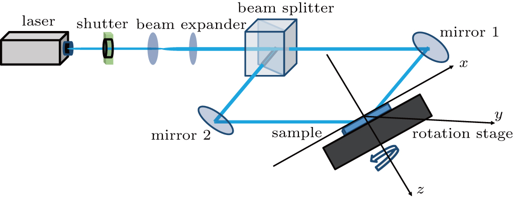
Figure 1 presents a schematic of the proposed micro-optical structure fabrication lithography method, which is based on sample rotation and two-laser-beam interference. Here, a He–Cd laser is assumed as the laser source. The He–Cd laser is typically used in LIL,[17] because it can emit lasers of two different wavelengths, i.e., 325 nm and 442 nm. In addition, the emitted laser can be easily converted from one wavelength to the other, while the beam propagation direction and the position in space remain unchanged. A shutter is used to control the exposure and a beam splitter is used to divide a single laser beam into two coherent parts. The sample is placed on a rotation stage.

Fig. 1. (color online) Schematic of lithography setup for micro-optical structure fabrication based on sample rotation and two-laser-beam interference.

It can be assumed that the two coherent light beams that emerge from the beam splitter are plane waves and can be modeled as

where and are the electric field amplitudes, and are the wave vectors, φ1 and are the initial phases, and and are the position vectors of the two beams, respectively. Furthermore, ω is the angular frequency of the waves and t is time. Thus, and represent the electric fields of the two beams.

Assume that the sample is fixed on the xy plane. Figure 2 shows the propagation of two laser beams emerging from the beam splitter in the xz plane. Thus, and are perpendicular to the y-axis and the propagating angles ( of the two beams relative to the z-axis are identical. We set . Thus, the electric fields along the x-axis on the sample surface can be expressed as

where . The superposition of the electric fields of the two individual plane waves gives

Fig. 2. (color online) Schematic of two-laser-beam interference on the sample surface, where and are the wave vectors and θ is the incidence angle.

The irradiance of the electromagnetic wave is given by . Thus, the spatial distribution of the total optical intensity of the two waves interfering on the sample is expressed as

To simplify the calculation process, we suppose ; thus, the intensity distribution can be expressed as
with the period of I(x) being

For a sample, two exposure methods are available. In one approach, N exposures are performed with sample rotations. In the other approach, the shutter retains opening and the sample is continuously exposed while being continuously rotated. By utilizing the coordinate transformation in matrix presentation,[31] the optical field distribution after the n-th rotation can be obtained, such that

where is the coordinate matrix of the optical field distribution after the n-th sample rotation and αn is the rotation angle relative to the first exposure. The initial optical field distribution is represented by . For N exposures, the total distribution can be expressed as

For the second exposure method, we assume that the angular velocity of the rotation is ω0; hence, the rotation angle can be expressed as a function of time, i.e., . Consequently, when the sample is rotating, the field distribution can be expressed as

If the total exposure time of the rotation process is T, the total optical field distribution can then be expressed as an integral

3. Numerical simulation results

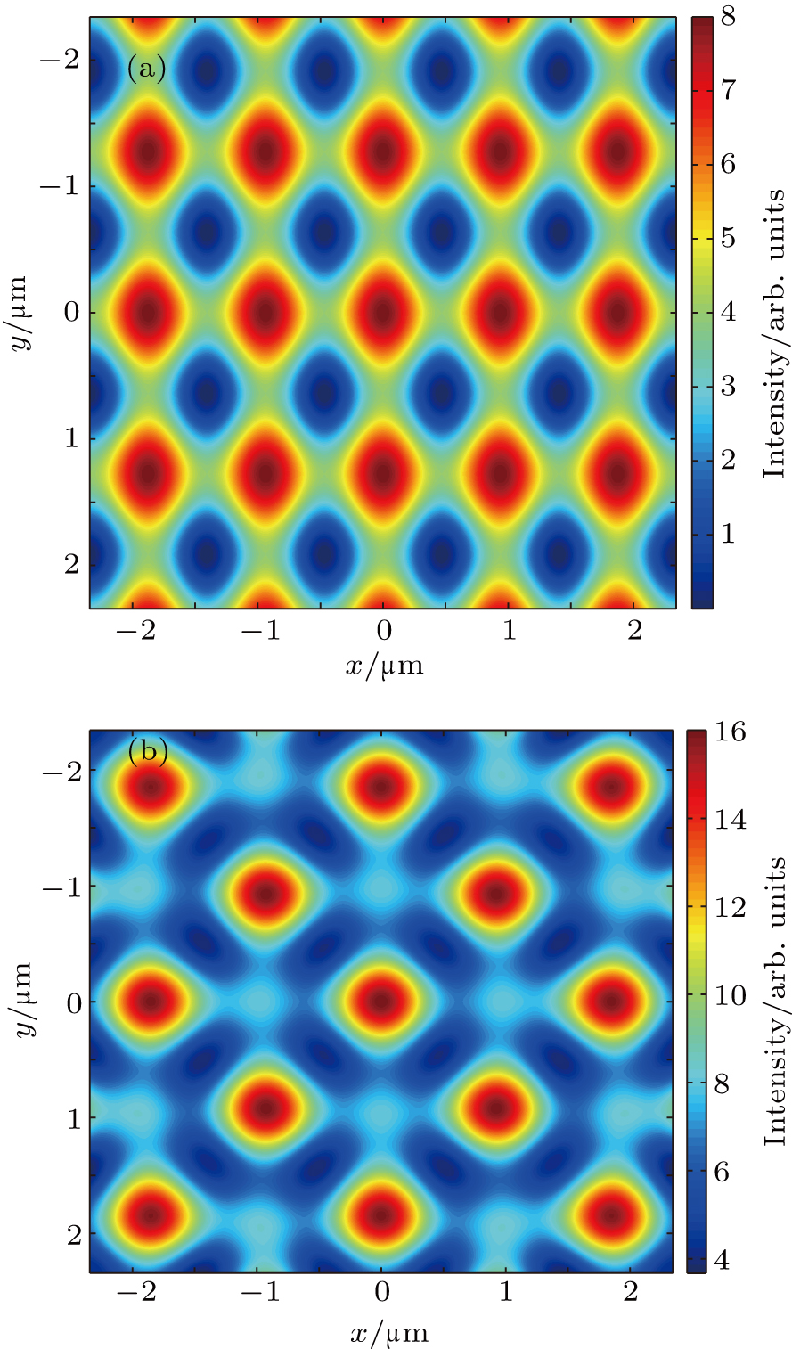
Based on the equations obtained above, we employ a numerical simulation to obtain the field distribution for a given rotation/exposure configuration, so as to theoretically demonstrate the corresponding micro-optical structure that could be fabricated in practice. A standing wave optical field distribution is formed via the interference of two coherent lasers according to Eq. (7); thus, a periodic 1D structure can be fabricated utilizing two-laser-beam interference. As an example, we use λ = 325 nm and θ = 10° in the simulation. The standing wave optical field distribution simulation results obtained for these parameters are shown in Fig. 3(a). Based on this distribution, a 1D grating with a period of 935.8 nm can be fabricated.

Fig. 3. (color online) (a) 2D optical field distribution for single exposure of two-laser-beam interference. (b) 2D optical field distribution for double exposure and 90°-rotated sample. (c) Magnified segment from panel (b).

Although the optical field distribution obtained from two coherent lasers is 1D, by exposing the photoresist sample and applying different rotation methods, we can fabricate numerous 2D micro-optical structures. As noted above, one approach is to expose the sample N times with sample rotations. If we rotate the sample by 90° and expose it for a second time with the same exposure dose, a 2D dot array pattern can be recorded on the photoresist sample. This case can be simulated using Eqs. (9) and (10), and the corresponding optical field distribution is shown in Fig. 3(b). A magnified segment of Fig. 3(b) is shown in Fig. 3(c); it is apparent that the dots of the array have a quasi-square shape. Furthermore, if the sample is subjected to three exposures under the same dose with a 60°-rotation after each exposure, a periodic hexagonal structure is obtained (Fig. 4(a)). From Fig. 4(b), a magnification of part of Fig. 4(a), it is apparent that there are six triangles outside this hexagonal structure. However, the optical field intensity of these triangles is very low compared to the hexagon. This difference is demonstrated by the 3D intensity distribution of one period shown in Fig. 4(c).

Fig. 4. (color online) (a) 2D optical field distribution for triple exposure, with the sample being rotated by 60° after each exposure. (b) Magnified segment from panel (a). (c) 3D optical field distribution of one period.

More interesting and complex structures can be fabricated by exposing and rotating the sample continuously. As an example, we simulate the total optical field distribution for the case in which the sample is continuously rotated with α = 180°, λ = 325 nm, and θ = 10°. An equally spaced concentric ring structure is obtained. Figure 5 shows the simulated results for the 2D and 3D optical field distributions. The intensity distribution along the center line of Fig. 5(a) is shown in Fig. 5(c). From the x-values of the crests and troughs, it can be determined that the loop width is approximately 936 nm, while the radius of the center round is 568 nm. From the graph of the distribution function and the 3D figure of the field distribution (Fig. 5(b)), it is apparent that the optical field of the rings decreases progressively. Further, the field at the center is extremely strong compared to that at the surrounding area.

Fig. 5. (color online) (a) 2D optical field distribution for continuous exposure, with the sample being continuously rotated by 180°. (b) 3D optical field distribution. (c) Optical field distribution along the x-axis. The numbers on the crests and troughs are the x-values.

As shown in Eq. (8), the period of the standing wave optical field distribution ( ) is proportional to λ. Therefore, by changing λ, we can fabricate micro-optical structures with vertical values different from the horizontal ones. To achieve this, the sample is first exposed to the 325-nm laser, before being rotated by 90°. The laser wavelength is changed from to , keeping as before. The sample is then exposed for the second time. The results of this procedure are shown in Fig. 6(a). It is obvious that the field distribution is similar to that shown in Fig. 3(b); however, the dots in Fig. 6(a) have a quasi-rectangular shape, with values of 935.8 nm and 1272.7 nm, whereas the dots in Fig. 3(b) are quasi square.

Fig. 6. (color online) (a) 2D optical field distribution for double exposure with different laser wavelengths (325 nm and 442 nm), where the sample rotation angle is 90°. (b) Quadruple exposure, where the wavelength of each exposure is 325 nm, 442 nm, 325 nm, and 442 nm respectively. The sample is rotated by 45° after each exposure.

Furthermore, by exposing the sample four times with 45° sample rotations after each exposure ( , 442 nm, 325 nm, and 442 nm, respectively), a more interesting structure can be obtained, as shown in Fig. 6(b). The distribution corresponds to an irregular quasi-trapezoidal lattice, but it is centrosymmetric. If we change the rotation and exposure method further, for example, by changing α or λ, additional micro-optical structures can be fabricated.

Various kinds of micro-optical structures can be fabricated using the proposed method, and the structure parameters can be controlled effectively by changing the laser-beam incidence angle and wavelength. The structures discussed above constitute selected examples of the various possibilities only.

4. Conclusion

We have proposed a method of fabricating micro-optical structures by employing sample rotation and two-laser-beam interference. By rotating and exposing a sample in different ways using the suggested interference device, a wide variety of micro-optical structures can be fabricated, such as hexagons and equally spaced concentric rings. By exposing the sample to lasers with different wavelengths, some irregular periodic optical structures can also be obtained. It is hoped that the proposed lithography method can be used for the fabrication of different kinds of micro-optical structures. Further, the micro-structures simulated in this study can be applied to numerous micro-optics fields. For example, the 1D grating can be used as a diffraction grating, the periodic hexagonal structure can be employed as a photonic crystal, and the spaced concentric rings can be used as a zone plate. Hence, the proposed technology will have considerable applications in the fields of micro- and nano-optics, because of its simple operation, low cost, and high output.

Reference
[1] Moon J H Ford J Yang S 2006 Polym. Advan. Echnol. 17 83
[2] Shibata S Che Y Sugihara O Okamoto N Kaino T 2004 Jpn. J. Appl. Phys. 43 2370
[3] Yu F Li P Shen H Mathur S Lehur C M Bakowsky U Mücklichd F 2005 Biomaterials 26 2307
[4] Liu Q Duan X M Peng C S 2014 Novel Optical Technologies for Nanofabrication Berlin Springer-Verlag 153 178
[5] Heyderman L J Solak H H David C Atkinson D Cowburn R P Nolting F 2004 Appl. Phys. Lett. 85 4989
[6] Snow E S Campbell P M 1994 Appl. Phys. Lett. 64 1932
[7] Harriott L R 2001 Proc. IEEE 89 366
[8] Hinsberg W Houle F A Hoffnagle J Sanchez M Wallraff G Morrison M Frank S 1998 J. Vac. Sci. Technol. 16 3689
[9] Brousseau E B Dimov S S Pha D T 2010 Int. J. Adv. Manuf. Tech. 47 161
[10] Hassanzadeh A Ho Wong K K 2009 Photonics North 2009 August 4, 2009 Quebec, Canada 73861
[11] Xie Z H Yu W X Wang T S Zhang H X Fu Y Q Liu H Li F Y Lu Z W Sun Q 2011 Plasmonics 6 565
[12] Sreekanth K V Murukeshan V M 2010 J. Vac. Sci. Technol. 28 128
[13] Yang F Chen X Cho E H Lee C S Jin P Guo L J 2015 Appl. Phys. Express 8 062004
[14] Wang R Wang X X Yang H Ye S 2016 Acta Phys. Sin. 65 094206 in Chinese
[15] Wang X X Zhang D G Chen Y K Zhu L F Yu W H 2013 Appl. Phys. Lett. 102 031103
[16] Wang R Wang X X Yang H Qi Y P 2017 Chin. Phys. 26 024202
[17] Xie Q Hong M H Tan H L Chen G X Shi L P Chong T C 2008 J. Alloys Compd. 449 261
[18] Seo J H Park J H Kim S I Park B J Ma Z Q Choi J Ju B K 2014 J. Nanosci. Nanotech. 14 1521
[19] Yang H F He H D Zhao E L Han J Hao J B Qian J G Tang W Zhu H 2014 Laser Phys. 24 065901
[20] Kim H Jung H Lee D H Lee K B Jeon H 2016 Appl. Opt. 55 354
[21] Hang W Q Dong T G Wang G Liu S L Huang Z M Miao X J Lv Q Qin C J 2015 Chin. Phys. 24 084205
[22] Siddique R H Hünig R Faisal A Lemmer U Hölscher H 2015 Opt. Mater. Express 5 996
[23] Jiang H B Zhang Y L Han D D Xia H Feng J Chen Q D Hong Z R Sun H B 2014 Adv. Func. Mater. 24 4595
[24] Xuan M D Dai L G Jia H Q Chen H 2014 Optoelectr. Lett. 10 51
[25] Xu J Wang Z B Zhang Z Wang D P Weng Z K 2014 J. Appl. Phys. 115 203101
[26] Lai N D Liang W P Lin J H Hsu C C Lin C H 2005 Opt. Express 13 9605
[27] Voisiat B Gedvilas M Indrišiūnas S Račiukaitis G 2011 Phys. Proc. 12 116
[28] Cheng L Lipson R H 2010 Laser Photon. Rev. 4 568
[29] Wang X X Wang X D Yang H Ye S Yu J L 2015 J. Func. Mater. 46 20132 in Chinese
[30] Hassanzadeh A Mohammadnezhad M Mittlerb S 2015 J. Nanophoton. 9 093067
[31] Boas M L 2006 Mathematical Methods in the Physics Science 3 Chichester John Wiley and Sons 126 130
[32] Born M Wolf E 1999 Principles of Optics 7 England Cambridge University Press 287 289