


Band structure of silicon and germanium thin films based on first principles
Cite this Article
Wu Xue-Ke, Huang Wei-Qi, Huang Zhong-Mei, Qin Chao-Jian, Dong Tai-Ge, Wang Gang, Tang Yan-Lin. Band structure of silicon and germanium thin films based on first principles. Chinese Physics B, 2017, 26(3): 037302 
Permissions
Band structure of silicon and germanium thin films based on first principles
† Corresponding author. E-mail:
Abstract
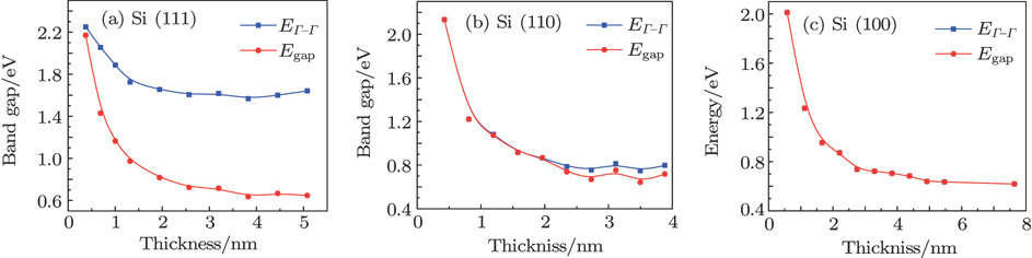
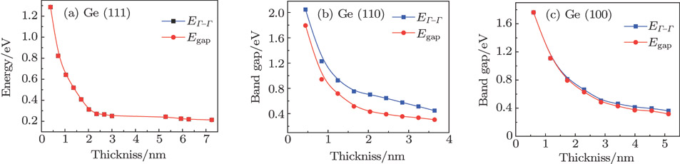
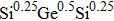
In nanomaterials, optical anisotropies reveal a fundamental relationship between structural and optical properties, in which directional optical properties can be exploited to enhance the performance of optoelectronic devices. First principles calculation based on density functional theory (DFT) with the generalized gradient approximation (GGA) are carried out to investigate the energy band gap structure on silicon (Si) and germanium (Ge) nanofilms. Simulation results show that the band gaps in Si (100) and Ge (111) nanofilms become the direct-gap structure in the thickness range less than 7.64 nm and 7.25 nm respectively, but the band gaps of Si (111) and Ge (110) nanofilms still keep in an indirect-gap structure and are independent on film thickness, and the band gaps of Si (110) and Ge (100) nanofilms could be transferred into the direct-gap structure in nanofilms with smaller thickness. It is amazing that the band gaps of Si 
1. Introduction
Due to indirect band gap materials, the luminescence efficiency of Silicon (Si) and germanium (Ge) is very low and its application is limited. However, in the past 20 years, since it has been found that a strong photoluminescence can be obtained with the direct bandgap characteristics in low dimensional nanostructures of Si and Ge,[1–6] the research of low dimensional nanostructures such as nanoparticles, nanowires, and superlattice of Si and Ge has become a very active field due to a broad application prospects in the advanced optoelectronic devices.[7–10]
The material optical characteristics are determined by the electronic states, and the electronic states and the band gap characteristics are changed in the energy band engineering. Previous research showed that the formation of nanostructure is one of the energy band engineering of Si and Ge. For example, Jensen et al. showed that the band gap of H, F, and OH terminated [110] Si nanowires with diameters up to 6.1 nm are direct band gap structures,[11] and Morishita et al. showed that the sp3 structure of the Si nanosheet is retained after functionalisation with the phenyl groups and leads to a direct band gap.[12] Taking into account a large number of experimental results for usually forming nanofilms, the electronic structures of hydrogen passivation nanofilms treated as an ideal quantum surface structure with one dimensional limit are investigated by using the first principle in the article.
2. Model and calculation method
The structure optimization and energy band structure calculations of Si and Ge nanofilms are based on density functional theory (DFT). The generalized gradient approximation (GGA) with the Perdew–Burke–Ernzerh (PBE) function is selected as the exchange and correlation potential.[13–15] For all the calculations, the ultrasoft pseudopotentials are used, the cut-off energy of 380 eV is assumed in the plane-wave basis set, the SCF convergence tolerance of electronic energy is 
The most representative Si (Ge) nanofilms in (100), (110), and (111) are selected as the research object, and the nanofilms with different thickness are set up. The unit cell, overhead view, and lateral view of Si (Ge) nanofilms are shown in Fig. 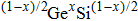


 | Fig. 1. (color online) Unit cells, overhead view, and lateral view of Si nanofilms with different orientations: (a) (100), (b) (110), and (c) (111). The Si and H atoms are represented by yellow and gray balls, respectively. |
 | Fig. 2. (color online) Optimized strctures of 4 unit cells thickness 
|
3. Results and discussion
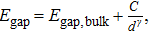
where C and γ are the fitting parameters, d is the thickness of Si film, and

is the band gap of bulk Si which is 0.599 eV by our calculation. The fitting results are shown in Table 1 , which are consistent with the previous theoretical calculation results and experimental results,[22–25] and further illustrate that the band gap changes obey the QC effect.
After geometry optimization, the lattice constant a and atomic bond length d of Si (111) face with one atom thick (silicene, 


 | Fig. 3. (color online) The energy level of Γ point (

|
After geometry optimization, the lattice constant a, atomic bond length d, and band gap of Ge(111) single atomic layer (


 | Fig. 4. (color online) The energy level of Γ point 

|
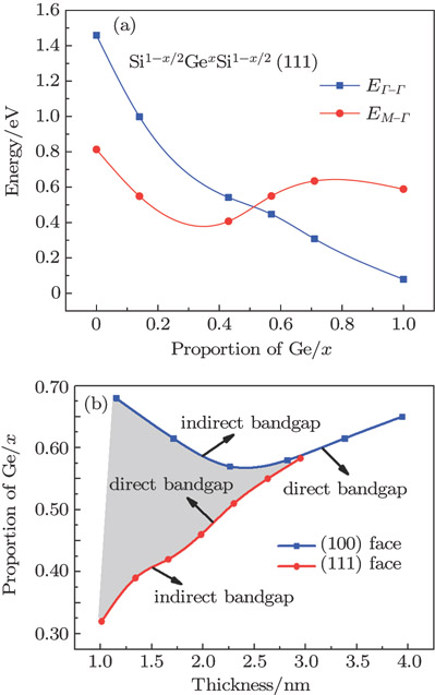
The direct band gap structure of Si (100) and Ge (111) films have common characteristics that the symmetry points in the directions of Si [100] and Ge [111] in k-space both correspond to the lowest energy valley in bulk materials, respectively.[12] The relationship among energy valleys in the conduction band of Si and Ge are 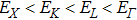
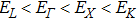
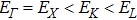
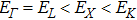


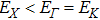
In Fig.
 | (1) |
| Table 1.
Fitting parameters for the band gap versus thickness curves using Eq. ( |
We calculate the band structure of 


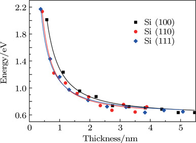 | Fig. 5. (color online) Fitting curves of band gap with change of thickness. |
 | Fig. 6. (color online) (a) Direct band gap transition to indirect band gap in 7 unit cells thickness of 

|
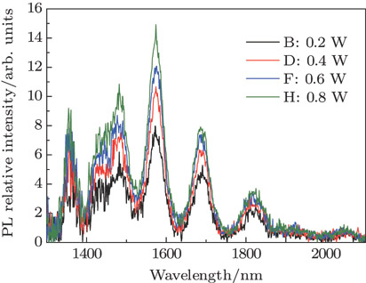
As shown in Fig.
 | Fig. 7. (color online) PL spectra in infrared wavelength measured on superlattice structure of Si–Ge layers in (111) direction at 20K. |
4. Conclusion
The thin films of Si, Ge, and 

Reference
| [1] | |
| [2] | |
| [3] | |
| [4] | |
| [5] | |
| [6] | |
| [7] | |
| [8] | |
| [9] | |
| [10] | |
| [11] | |
| [12] | |
| [13] | |
| [14] | |
| [15] | |
| [16] | |
| [17] | |
| [18] | |
| [19] | |
| [20] | |
| [21] | |
| [22] | |
| [23] | |
| [24] | |
| [25] |