† Corresponding author. E-mail:
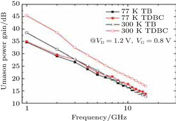
Radio-frequency (RF) characteristics under ultra-low temperature of multi-finger partially depleted silicon-on-insulator (PD SOI) n-type metal–oxide–semiconductor field-effect transistors (nMOSFETs) with tunnel diode body-contact (TDBC) structure and T-gate body-contact (TB) structure are investigated in this paper. When operating at 77 K, TDBC device suppresses floating-body effect (FBE) as well as the TB device. For TB device and TDBC device, cut-off frequency (fT) improves as the temperature decreases to liquid-helium temperature (77 K) while that of the maximum oscillation frequency (fMAX) is opposite due to the decrease of the unilateral power gain. While operating under 77 K, fT and fMAX of TDBC device reach to 125 GHz and 77 GHz, representing 8% and 15% improvements compared with those of TB device, respectively, which is mainly due to the lower parasitic resistances and capacitances. The results indicate that TDBC SOI MOSFETs could be considered as promising candidates for analog and RF applications over a wide range of temperatures and there is immense potential for the development of RF CMOS integrated circuits for cryogenic applications.
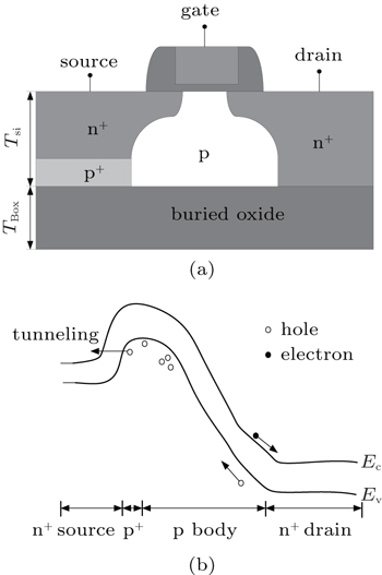
Silicon-on-insulator (SOI) technology has become more popular as a potential technology for low-power microwave circuits due to the advantages of the improved frequency performance through reduced capacitance, high mobility, and a reduction in the interconnect length, compared with bulk-Si technology.[1] Because of lower parasitic gate capacitance, the floating body (FB) structure has better frequency performance compared with body contact structures.[2] However, the main concern for FB structure is the floating body effect (FBE) caused by the impact-ionization under high drain voltage. FBE limited the application of partially depleted (PD) SOI metal–oxide–semiconductor field-effect transistors (MOSFETs) in analog circuits and RF circuits due to Kink effect.[3] In addition, the body potential instability and an abnormal subthreshold swing, caused by FBE, are also disadvantageous factors.[4] To suppress FBE in PD SOI MOSFETs, body contact methods with different structures have been proposed, such as T-gate body contact (TB) structure, H-gate body contact (HB) structure, and so on. The tunnel diode body contact (TDBC) structure was proposed to suppress FBE and improve RF performance by using a tunnel diode under the source region.[5] In contrast from the conventional body contact structure, TDBC structure efficiently suppresses FBE and body-instability problems with smaller areas compared with TB structure and achieves better fT and fMAX with respect to smaller parasitic gate-source capacitance.[6] The TDBC structure also shows excellent immunity of back gate bias effect[7] compared with FB and TB devices. Most importantly, the fabrication process of TDBC structure is fully compatible with the usual SOI CMOS technology.
Small signal ac performances of multi-finger PD SOI nMOSFET with TDBC structure and conventional TB structure manufactured by employing a 0.13-μm SOI CMOS technology are investigated at 77 K and 300 K. Moreover, the stability factors of devices based on the small-signal model parameters are derived and the effects of temperature are also investigated for RF applications.
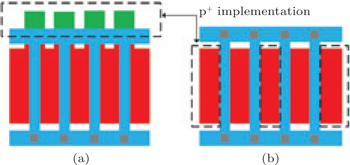
The multi-finger PD SOI nMOSFETs with TDBC structure and TB structure are fabricated in 0.13-μm SOI CMOS technology to investigate the RF performance. The devices designed with multi-fingers investigated in this paper have the same dimensions: the gate length is 0.13 μm and the total width is 20 μm. The unit finger width is 5 μm and the finger number is 4. The thicknesses for silicon film (Tsi) and buried oxides (Tbox) for the devices are 100 nm and 145 nm, respectively. For the TB device, p+ implantation is performed to form the p+ body contact area. Figure
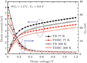
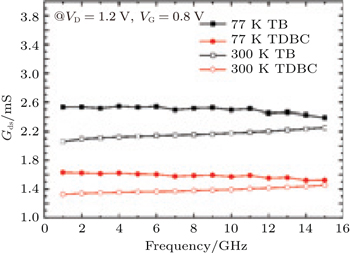
The devices were used to perform a S-parameter measurement under liquid-helium temperature (77 K) and room temperature (300 K) from 1 GHz to 15 GHz. To extract the practical performance of the devices, the measured S-parameters are de-embedded using open and short de-embedding structures. Threshold voltage (Vth) of TDBC, and TB device extracted when the drain current equals 0.1W/L μA (W is the total gate width, L is the gate length) at a constant drain voltage (Vd = 1.2 V) is 0.38 V, and 0.306 V at 77 K and 0.241 V, and 0.176 V at 300 K, respectively. The reason for the higher threshold of TDBC is the boron diffused into the channel region at the anneal stage. The output characteristic and drain conductance (Gds) of the devices under different temperatures when Vg is 0.8 V is shown in Fig.
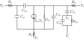
To compare the small signal characteristics of TB and TDBC devices, a simple small signal equivalent circuit is illustrated in Fig.


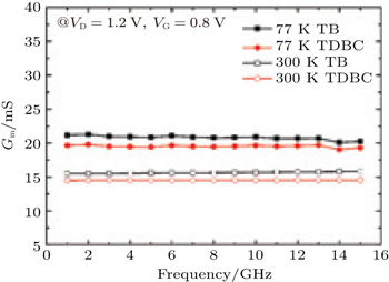
Figure
Due to the design rules limiting that the gate contact was forbidden upon active region, the gate of TDBC device is contacted from both sides and TB device is contacted from only one side, as shown in Fig.
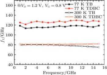
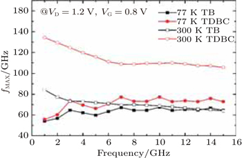
The cut-off frequency (fT) and the maximum oscillation frequency (fMAX) are important figures of merit to quantify the RF performance of a transistor.[10] The fT is the frequency when the drain current gain equals to one, and fMAX is the frequency when the power gain is unity. The physics background of fT and fMAX can be expressed as follows:[11]


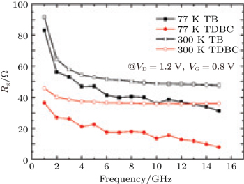 | Fig. 7. Gate resistance Rg as a function of frequency at 300 K and 77 K for TB and TDBC devices, respectively. |
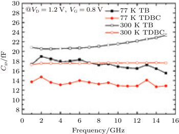 | Fig. 8. Gate-to-source capacitance (Cgs) as a function of frequency at 300 K and 77 K, respectively. |
Due to lower parasitic resistances and capacitances, the device with TDBC structure represents 15% improvement in fMAX and 8% improvement in fT compared with TB devices at 77 K respectively, as shown in Figs.
The RF performances of multi-finger PD SOI nMOSFETs with TDBC structure and conventional TB structure at 77 K and 300 K are compared in this paper. By using a simple small signal equivalent circuit model, the extracted small signal parameters of two types of devices are discussed to evaluate the influence on RF performance. The cut-off frequencies (fT) of TB and TDBC devices show ∼50% and ∼60% improvement compared with those at 300 K. The improvement in fT happens because of the improvement in trans-conductance and the decrease of gate capacitance. By contrast with the behavior of fT, maximum oscillation frequency (fMAX) decreases as the temperature decreases. For TB and TDBC devices, the most possible reason for this degradation is resulting from the increase of Gds and Cgd, while the TDBC shows more significant degradation does than TB. However, the degradation in fMAX, TDBC still shows ∼15% improvement than TB. The significant high-frequency characteristics of TDBC device under both the two temperatures indicate that the TDBC SOI MOSFETs are a good candidate for the analog and RF application over a wide range of temperatures. Moreover, based on the measured data, the significant high-frequency performance at 77 K indicates that there is immense potential for the development for cryogenic applications.
| 1 | |
| 2 | |
| 3 | |
| 4 | |
| 5 | |
| 6 | |
| 7 | |
| 8 | |
| 9 | |
| 10 | |
| 11 | |
| 12 |


