† Corresponding author. E-mail:
Project supported by the National Natural Science Foundation of China (Grant Nos. 51327001 and 51636002), and partially supported by CREST, JST, and JSPS KAKENHI (Grant Nos. 16H04280, 26289047, 16K14174, and 16K06126).
Metallic nanofilms are important components of nanoscale electronic circuits and nanoscale sensors. The accurate characterization of the thermophysical properties of nanofilms is very important for nanoscience and nanotechnology. Currently, there is very little specific heat data for metallic nanofilms, and the existing measurements indicate distinct differences according to the nanofilm size. The present work reports the specific heats of 40-nm-thick suspended platinum nanofilms at 80–380 K and ∼5×10⁻⁴ Pa using the 3ω method. Over 80–380 K, the specific heats of the Pt nanofilms range from 166–304 J/(kg·K), which are 1.65–2.60 times the bulk values, indicating significant size effects. These results are useful for both scientific research in nanoscale thermophysics and evaluating the transient thermal response of nanoscale devices.
Metallic nanofilms are important components of nanoscale electronic circuits, nanoscale sensors, and nano-electro-mechanical systems (NEMS). The accurate thermophysical characterization of metallic nanofilms is a key issue for both nanoscience and nanotechnology. Specifically, suspended metallic nanofilms have been used as resistive thermometers to probe nanoscale steady-state thermal and thermoelectric transport in the well-developed T-type method[1–4] and the H-type thermal bridge method.[5,6] In these methods, the in-plane electrical and thermal conductivities of the metallic nanofilm itself are prerequisites that are calibrated in advance using the direct current self-heating method.[7–9] In this electrical self-heating method,[7–9] the suspended metallic nanofilms are integrated with four probing electrodes, and a one-dimensional heat conduction model is used to effectively describe the direct current self-heating process, while the average temperature of the nanofilm is obtained from its own temperature-dependent resistance. The electrical and thermal conductivities of suspended metallic nanofilms have been measured many times,[1–9] and the results are distinctly different from the corresponding bulk values. The electrical and thermal conductivities of suspended 40-nm-thick platinum nanofilms were found to be less than half of the bulk values,[1–4,7–9] a fact that is explained by the surface and grain boundary scatterings.[8,9]
The specific heat of metallic nanofilms has seldom been investigated, although the specific heat is an important quantity when using metallic nanofilms to probe nanoscale transient thermal transport. In a theoretical study, Chen and Dames[10,11] used the low-dimensional Debye sub-model for elastic continuum boxes to simulate the temperature-dependent specific heat of low-dimensional materials. In this sub-model, the key parameters for determining the specific heat are the sound velocity, geometry, and the boundary conditions (fixed, free, or periodic). The results showed that the temperature-dependent specific heat follows a power law with respect to the temperature at low temperatures, where the power law exponent equals the dimensionality. Below 10 K, the specific heat of 1D materials is one order higher than that of 2D materials and two orders higher than that of 3D materials, whereas the specific heats of 1D, 2D, and 3D materials are nearly the same above 100 K. The simulation results were in accordance with the measured specific heats of TiO2 nanotubes.[10] Experimentally, Yu et al.[12–14] developed a microscale calorimeter and measured the specific heats of 20–340-nm-thick Cu and 40–1150-nm-thick Al nanofilms supported on Si wafers in a vacuum. The results showed that the specific heats of Cu and Al nanofilms increase with decreasing thickness. At 300 K, the specific heat of the Cu nanofilm was 10% higher than the bulk value when the thickness was 100 nm and 65% higher when the thickness was 20 nm, whereas the specific heat of the Al nanofilm was 42% higher than the bulk value when the thickness was 40 nm. Yu et al.[13,14] further simulated the specific heats of Cu and Al nanofilms with < 10 nm thickness, and attributed the enhancement in specific heat to the softening of phonons at the grain boundaries and the increased thermal expansion coefficient. Lugo et al.[15,16] measured the specific heats of Al, Au, and Cu nanofilms supported on glass at room temperature and atmospheric pressure based on the nanofilms’ transient response to pulse currents, and reported that the specific heats of 20-nm-thick Al, Au, and Cu nanofilms were, respectively, 1.60, 1.78, and 1.58 times that of the corresponding bulk values, suggesting significant size effects. However, Queen and Hellman[17] reported no size effects on the specific heats of metallic nanofilms. They measured the specific heats of 52.5-nm-thick, 30.3-nm-thick Cu and 54.6-nm-thick Au nanofilms supported on SiNx using a SiNx-based nanoscale calorimeter, and obtained specific heats almost the same as the bulk values. Currently, there are still very few data for the specific heats of metallic nanofilms, and the existing measurements indicate variable size effects. Therefore, more measurements are required to evaluate the size effects of the specific heats of metallic nanofilms. In addition, the measured samples in previous studies were supported on Si, SiNx, or glass substrates, and there is a lack of experimental data on the specific heats of suspended samples, which are widely used as nanoscale sensors. Moreover, the specific heats of suspended nanofilms can differ from those of supported ones because of surface interactions, and thus it is necessary to experimentally investigate the specific heats of suspended metallic nanofilms.
The 3ω measurement method[18–21] is effective for simultaneously measuring the thermal conductivity and specific heats of suspended wires, and has been widely applied in measuring the specific heat of microscale wires. In the 3ω method, an alternating current with 1ω frequency is used to heat the suspended sample, and the thermal conductivity and specific heat can be simultaneously extracted from the frequency-dependent 3ω signals. The present paper reports the measurement of specific heats of 40-nm-thick suspended platinum nanofilms at 80–380 K using the 3ω method.
In the 3ω method, an alternating current with 1ω circular frequency is passed through a suspended nanofilm, and the electrical power varies at a frequency of 2ω. This results in a 2ω vibrating temperature rise in the nanofilm.[18–21] Because the electrical resistance of the Pt nanofilm varies linearly with temperature, the electrical resistance of the suspended nanofilm will also vary at 2ω and give rise to a 3ω voltage. The thermal conductivity and specific heat can be simultaneously extracted from the relationship between the 3ω voltage and the frequency.[18–21] As for the heat conduction model, because the length of the nanofilm is much larger than the width and thickness, the heat conduction process in the suspended Pt nanofilm can be described by a 1D transient diffusive equation with a volumetric heat source, and the 3ω voltage can be derived from the average temperature rise of the suspended nanofilm. When the input current is I = I1sin(ωt), the 3ω voltage of the suspended Pt nanofilm, V3ω, is expressed by[19]


In practice, it is more common and convenient to use a voltage source instead of a current source. In this case, the resistance fluctuation of the sample should be much less than the total resistance in the circuit to guarantee the current source assumption applied in the above formulas.
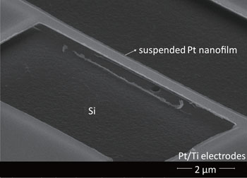
Suspended platinum nanofilms were fabricated via a series of nanofabrication processes, mainly consisting of electron beam lithography (EBL), electron-beam-induced physical vapor deposition (EB-PVD, Showa Shinku SEC-12), and etching processes on the Si wafer. First, a 320-nm-thick EBL resist, ZEP520-A, was spin coated on a 1 cm × 1 cm Si wafer with 260-nm-thick SiO2, and a pattern with four electrodes and a narrow ribbon was developed in the EBL resist. Second, 8-nm-thick Ti and ∼ 40-nm-thick Pt layers were successively deposited on the Si wafer by EB-PVD, with the Ti layer used as adhesive material between the Pt and the Si wafer. The electron beam voltage was 8 kV and the purities of the Ti and Pt were 99.99% and 99.98%, respectively. The EBL resist and the metal on the resist were then removed during the liftoff process, leaving the metallic nanofilm with the electrode–nanowire patterns on the Si wafer. Finally, the narrow Pt nanofilm was suspended by etching the Ti and SiO2 underneath the nanowire using 37% buffered HF and further etching the Si via CF4 plasma. The total etching depth was about 1 μm. Figure
| Table 1. Dimensions of the three measured suspended Pt nanofilms. . |
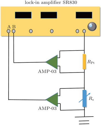
The 3ω signals were collected using a commercial lock-in amplifier (Stanford Research SR830) with a maximum output 1ω frequency of 34 kHz. The measurement system was established based on a previous study[20] and the electrical circuit is shown in Fig.
During the measurement process, the resistance box was adjusted to equal the electrical resistance of the test Pt nanofilm. The 1ω signals of the test nanofilm and the resistance box were set to be the same, and the signal noise in the circuit was eliminated by subtracting the signals of the test nanofilm and the resistance box.[20,21] Additionally, the current was controlled to within 200 μA and the temperature fluctuation to within 5 K, so that the resistance fluctuation was less than 0.3% of the total resistance in the circuit, thus ensuring that the current source assumption was satisfied.
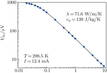
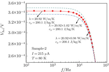
Before taking measurements, a suspended Pt wire of 30 μm diameter and 20.2 mm length was measured to validate the 3ω measurement system. Figure
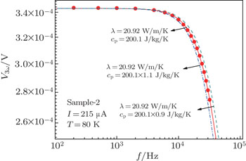
According to Eq. (
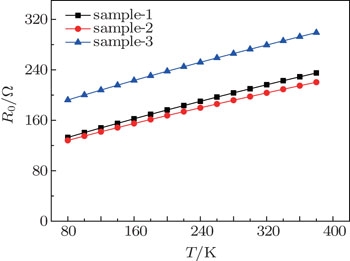
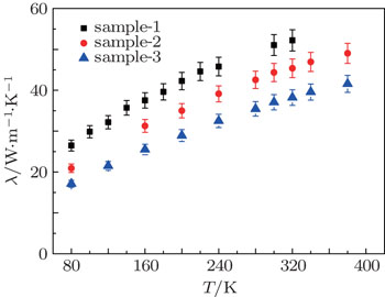
The thermal conductivities of the three samples obtained by the V3ω–f curve fitting method are shown in Fig.
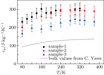
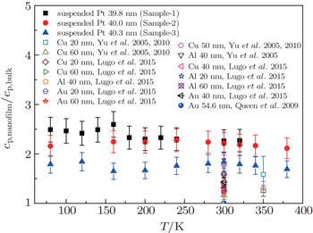
Figure
According to Yu et al.,[10–12] the enhancement of the specific heats of metallic nanofilms can be mainly attributed to two factors. First, the softening of phonons at the surfaces or grain boundaries enhances the specific heat of a constant volume cv, which means that the atoms at the surface or grain boundaries need more heat input to increase the temperature. Second, the grain boundaries and defects in the nanoscale crystalline structure significantly increase the thermal expansion coefficient, causing further enhancement of cp because the nanofilm needs more energy to perform the work of expansion. Therefore, compared with the bulk material, nanofilms need more heat input to increase internal energy and perform the necessary expansion work because of the important role of the atoms at the surfaces and grain boundaries. For the suspended nanofilms measured in the present work, the effects of the surface atoms are more significant, because there are two free surfaces, and thus the specific heats of the suspended nanofilms are even larger than those of supported nanofilms.
The uncertainties of the dimension measurements were less than 1%. The collected 3ω signals had a 4-digit resolution and uncertainties of less than 0.3%. The main uncertainty comes from the two-parameter fitting process using Eqs. (
This study investigated the specific heats of suspended 40-nm-thick Pt nanofilms at 80–380 K and ∼ 5×10⁻⁴ Pa. The specific heats of three measured samples ranged from 166–304 J/(kg·K) over 80–380 K, which are 1.65–2.60 times the bulk values. At 300 K, the specific heats of the three samples were 301 J/(kg·K), 294 J/(kg·K), and 245 J/(kg·K), some 1.8–2.3 times the bulk value, indicating significant size effects. These results are useful for scientific research in nanoscale thermophysics and the design of nanoscale devices for transient thermal response.
| 1 | |
| 2 | |
| 3 | |
| 4 | |
| 5 | |
| 6 | |
| 7 | |
| 8 | |
| 9 | |
| 10 | |
| 11 | |
| 12 | |
| 13 | |
| 14 | |
| 15 | |
| 16 | |
| 17 | |
| 18 | |
| 19 | |
| 20 | |
| 21 | |
| 22 |


