


X-band inverse class-F GaN internally-matched power amplifier
[Zhao Bo-Chao1, Lu Yang1, Han Wen-Zhe1, Zheng Jia-Xin2, Zhang Heng-Shuang1, Ma Pei-jun1, †,  , Ma Xiao-Hua2, Hao Yue1, 2]
, Ma Xiao-Hua2, Hao Yue1, 2]
|
|

 , Ma Xiao-Hua2, Hao Yue1, 2
† Corresponding author. E-mail:
Project supported by the National High Technology Research and Development Program of China (Grant No. 2015AA016801).
An X-band inverse class-F power amplifier is realized by a 1-mm AlGaN/GaN high electron mobility transistor (HEMT). The intrinsic and parasitic components inside the transistor, especially output capacitor Cds, influence the harmonic impedance heavily at the X-band, so compensation design is used for meeting the harmonic condition of inverse class-F on the current source plane. Experiment results show that, in the continuous-wave mode, the power amplifier achieves 61.7% power added efficiency (PAE), which is 16.3% higher than the class-AB power amplifier realized by the same kind of HEMT. To the best of our knowledge, this is the first inverse class-F GaN internally-matched power amplifier, and the PAE is quite high at the X-band.
GaN high electron mobility transistors (HEMTs) have advantages in breakdown voltage, power density, and high electron, so they are good choices for high-frequency high-efficiency power amplifiers.[1–3] Smaller in size compared with a hybrid microwave integrated circuit (HMIC) and better in thermal performance compared with a monolithic microwave integrated circuit (MMIC), the internally-matched power amplifier is a competitor for C-band and X-band applications. Class-F and inverse class-F[4] are two important ways to improve power added efficiency (PAE) in design. Their principles are both that: output impedances at fundamental and harmonic frequencies are presented appropriately, so the output current and voltage waveforms are shaped to minimize the power dissipation and then more power is carried out.
Several high efficiency GaN-based power amplifiers have been presented. In 2009, Helaoui et al.[6] designed an L-band 81% PAE class-F power amplifier. In 2011, Kim et al.[7] manufactured S-band 69.9% PAE class-F and 69.4% PAE inverse class-F power amplifiers. We also increased the PAE of the GaN-based internally-matched power amplifier to 71% at 4 GHz[8] and 69% at 5.5 GHz.[9] At X-band applications, Resca et al.[10] reported a GaN MMIC power amplifier with 38% PAE for future generation synthetic aperture radar (SAR) systems. Waltereit et al.[13] developed a 50% PAE GaN MMIC with life times above 105 h for space applications. However, the power amplifier with PAE over 60% at the X-band is rarely seen because of the heavy parasitic effects.
In this paper, the compensation design of an X-band inverse class-F internally-matched power amplifier is used based on GaN HEMTs with 1-mm gate width. The second harmonic open and the third harmonic short are achieved on the current source plane. Under the continuous-wave condition, the amplifier achieves a high PAE of 61.7% at 8.1 GHz with an output power of 6.7 W. The rest of this paper is structured as follows: Section 2 introduces the basic principle of inverse class-F PA. The compensation design and simulation of the inverse class-F are shown in Section 3. Experiment results and comparisons with class-AB and other works are shown in Section 4. The conclusion is in Section 5.
An HEMT is essentially a voltage-controlled current source. Seen from the current source plane, the voltage and current waveforms of the ideal inverse class-F power amplifier are shown in Fig.
The next question is how to realize the waveform shown in Fig.

 | Fig. 1. Current and voltage waveforms of the inverse class-F PA in the ideal case and in the case when only the second and the third harmonics are controlled, respectively. |
Generally, only the second and third harmonics are controlled in inverse class-F design, as it is very complex and there is less contribution to efficiency to control the harmonics with an order higher than third. The waveform under this condition is shown in Fig.
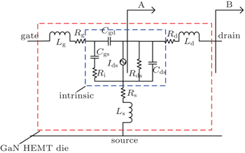
The 1-mm gate width GaN HEMT was fabricated at Xidian University, China.[9] The basic model is shown in Fig.
 | Fig. 2. Typical GaN HEMT model. “B” is the drain pad plane and “A” is the current source plane. |
It is assumed that the inverse class-F impedance condition where the second harmonic open and the third harmonic short are realized on plane “B”, figure
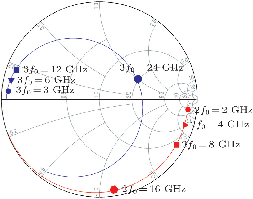 | Fig. 3. The second and third harmonic impedance on plane “A” (shown in Fig. |
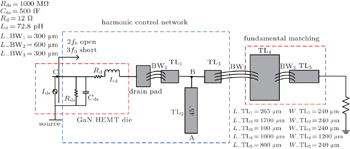
The schematic structure of the output harmonic control network and fundamental matching network is shown in Fig.
 | Fig. 4. Output harmonic control network and fundamental matching network. Second harmonic open and third harmonic short are achieved on the current source plane. |
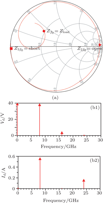
 | Fig. 5. Fundamental, second, and third harmonic impedance on the current source plane (a). Frequency spectrum of voltage (b1) and current (b2) on the current source plane. |
The simulated impedance is shown in Fig.
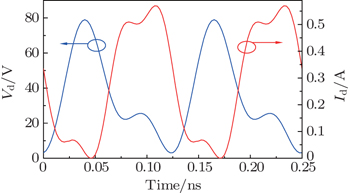
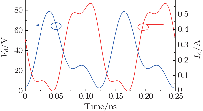 | Fig. 6. Simulated waveforms of current and voltage on the current source plane. |
The matching modules are soldered in a package with a cavity size of 14.5 mm × 14.8 mm. The 1-mil (1 mil = 0.0254 mm) diameter bonding wires connect the modules, participating in the match at the same time. Due to the manufacturing error and model error, the lengths of BW1 and BW2 can tune the second and third harmonics respectively (the MMIC power amplifier cannot be tuned after being fabricated). The photograph of the proposed X-band inverse class-F power amplifier is shown in Fig.
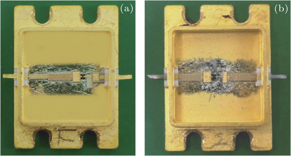 | Fig. 7. Photographs of the proposed X-band inverse class-F power amplifier (a) and the compared X-band class-AB power amplifier (b). |
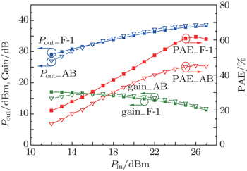
The two power amplifiers are measured under the continuous-wave operation. The DC bias condition is VDS = 40 V and IDS = 60 mA. As described in Fig.
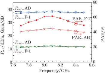
The frequency response of the two power amplifiers is also shown in Fig.
As a power amplifier product, the last process is parallel seam sealing to achieve high quality and long term reliability. After the sealing process, the variation of gain and PAE is less than 0.1 dB and 0.2%.
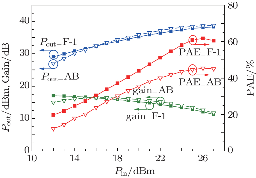 | Fig. 8. Measured microwave performance of the power amplifier in continuous mode at 8.1 GHz. The output power Pout, gain, and PAE are compared between inverse class-F and class-AB power amplifiers. |
 | Fig. 9. Measured microwave performance of the power amplifier in continuous mode when input power is 26 dBm. The Pout, gain, and PAE are compared between inverse class-F and class-AB power amplifiers. |
The comparison between the proposed inverse class-F power amplifier and other works is shown in Table
| Table 1. The high efficiency power amplifier at different frequency bands. . |
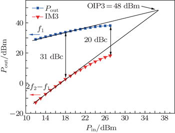
Two-tone measurements are also performed to characterize the linearity of the inverse class-F power amplifier. As shown in Fig.
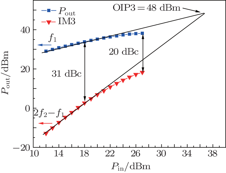 | Fig. 10. Measured linearity performance using two-tone signal. Here, f1 = 8.05 GHz and f2 = 8.15 GHz. |
An X-band 61.7% PAE inverse class-F power amplifier is presented. A harmonic control network is used for compensating the components inside the transistor model, so the inverse class-F impedance condition is obtained on the current source plane. The harmonic impedance can be tuned by the bonding wires (BW1, BW2) and the compensation design can also be used in large gate width HEMT internally-matched power amplifiers. To the best of our knowledge, this is the first inverse class-F GaN internally-matched power amplifier, and the PAE is relatively high in X-band applications.
| 1 | |
| 2 | |
| 3 | |
| 4 | |
| 5 | |
| 6 | |
| 7 | |
| 8 | |
| 9 | |
| 10 | |
| 11 | |
| 12 | |
| 13 | |
| 14 |