Preparation of patterned boron nanowire films with different widths of unit-cell and their field emission properties
Zhang Yong-Xin1, Liu Fei2, Shen Cheng-Min1, †, , Li Jun1, Deng Shao-Zhi2, Xu Ning-Sheng2, Gao Hong-Jun1, ‡,
Beijing National Laboratory for Condensed Matter Physics, Institute of Physics, Chinese Academy of Sciences, Beijing 100190, China
State Key Laboratory of Optoelectronic Materials and Technologies, Guangdong Province Key Laboratory of Display Material and Technology, and School of Microelectronics, Sun Yat-sen University, Guangzhou 510275, China


† Corresponding author. E-mail: cmshen@iphy.ac.cn

‡ Corresponding author. E-mail: hjgao@iphy.ac.cn

Project supported by the National Basic Research Program of China (Grant Nos. 2013CB933604), the National Natural Science Foundation of China (Grant No. 51572290), and the Fund from the Chinese Academy of Sciences (Grant Nos. 1731300500015 and XDB07030100).

Abstract
Abstract

Large-area patterned films of boron nanowires (BNWs) are fabricated at various densities by chemical vapor deposition (CVD). Different widths of unit-cell of Mo masks are used as templates. The widths of unit-cell of Mo masks are 100 μm, 150 μm, and 200 μm, respectively. The distance between unit cells is 50 μm. The BNWs have an average diameter of about 20 nm and lengths of 10 μm–20 μm. High-resolution transmission electron microscopy analysis shows that each nanowire has a β-tetragonal structure with good crystallization. Field emission measurements of the BNW films show that their turn-on electric fields decrease with width of unit-cell increasing.

1. Introduction

For flat-panel field emission display devices, the pattern growth of cold cathodes based on quasi-one-dimensional nanoscale materials is becoming increasingly important because patterning can dramatically improve field emission (FE) properties and increase the FE enhancement factor by reducing screening effects between units of nanomaterials.[1,2] Boron bonds through a unique three-center two-electron bond make it possible to form the B12 icosahedron structural unit.[3] Therefore, boron possesses chemical stability and many desirable physical properties, such as low density, high melting point, and hardness comparable to diamond.[4,5] Moreover, it has a large tensile strength and high Young's modulus and a negative high-temperature electrical resistivity. Boron one-dimensional (1D) nanostructure, as a cold cathode material, has exhibited superior FE performances.[6]

The morphology of a boron nanostructured cold material, such as aspect ratio and density, can affect its FE properties. Therefore, preparation of patterned boron 1D nanostructure is important for improving the FE behavior.[7,8] In recent decades, various patterned 1D nanostructures have been fabricated by different means.[913] The patterned 1D nanostructures have also shown superior field emission properties. Compared with random-growth 1D nanostructured film, patterned structure has a lower turn-on field and threshold field. These results indicate that the FE property is significantly improved. In our group, patterned boron nanostructures have been synthesized by self-assembly of magnetic catalyst nanoparticles and a pre-manipulation to pattern the catalyst with a grid template serving as a mask.[14,15] In this present work, we use different widths of unit-cell of Mo masks as templates to tune the patterned distribution densities of boron nanowires. The results of field emission measurements of patterned BNWs with different unit-cell sizes indicate that their turn-on electric field decreases with increasing the width of unit-cell in the patterning.

2. Experiment
2.1. Materials

Boron powder (with purity 99.99%), B2O3 (99.99%), and carbon powder (99.9%) were purchased from Beijing Sinopharm Chemical Reagent Co. Argon (99.9%) and H2/Ar (H2, 10 vol%) were purchased from Beijing Praxair Application Gas Co., Ltd. Boron powder, B2O3, and carbon powder with mass ratio of 4:2:1 were mixed together as precursors.

2.2. Preparation of patterned B nanowires

The patterned BNWs were fabricated by the template method used in our previous reports.[15,16] A detailed description is as follows: different widths of unit-cell of Mo masks (100, 150, and 200 μm) were fixed on the surfaces of Si (111) wafers; then, 100-μL Fe3O4 hexane solution (20 mg/mL) was dropped on the Mo mask, coating the Si substructure and heated at 100 °C for 60 min; finally, the Mo mask was removed from the surface of the Si substrate, uncovering the patterned catalyst substrate. We used chemical vapor deposition (CVD) to grow patterned BNWs. The Si wafer patterned with Fe3O4 catalyst nanoparticles was placed in an alumina boat, lying in front of the precursors. Then, the alumina boat was transferred into a quartz tube in a horizontal tube furnace. After the system was pumped below 10 Pa, 50 sccm (standard cubic centimeters per minute) H2/Ar mixed gas (10%, volume ratio %) was introduced and system pressure was changed to 1 × 10² Pa. Then the furnace was heated to 1150 °C at a rate of 8 °C/min and the system pressure was maintained at 1 × 10⁴ Pa. The reaction was allowed to continue for 2 h at this temperature. The furnace was cooled down to room temperature at a rate of 8 °C/min. Brown–black products were found on the Si substrate.

2.3. Characterization of BNWs

The morphology and the structure of the BNWs were characterized by field emission scanning electron microscopy (FE-SEM: SFEG, FEI Corp), transmission electron microscopy (TEM: Tecnai-20, Philips Corp.), and high resolution transmission electron microscopy (HRTEM: Tecnai F20, FEI Corp.), respectively. Measurements of the field emission (FE) properties of patterned BNWs were performed on a high vacuum FE analysis system (4 × 10− 5 Pa).

3. Results and discussion

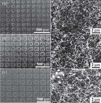
Figure 1 shows typical SEM images of patterned BNWs with different widths of unit-cell. From Fig. 1 it can been seen clearly that large-area, densely patterned BNWs are prepared using different widths of unit-cell of Mo masks as templates. The widths of unit-cell are 100 μm, 150 μm, and 200 μm, respectively. The distance between unit cells is 50 μm in all samples. No BNWs could be found at the bottoms of the channels between patterned units. The higher magnification SEM images are shown in Figs. 1(d)1(f), corresponding to widths of unit-cell 100 μm, 150 μm, and 200 μm, respectively. BNWs fully cover the surface of the Si (111) substrate. The results indicate that BNWs are packed densely on each square of the pattern. These nanowires have about 10 μm–20 μm in length and a diameter of 20 nm each.

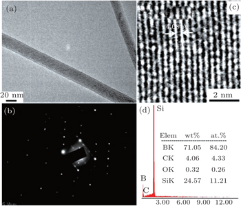
Further structure characterizations of BNWs are performed by transmission electron microscopy (TEM), high-resolution transmission electron microscopy (HRTEM), and selected area electron diffraction (SAED). Figure 2(a) shows a TEM image of BNWs. Each BNW has a smooth surface and diameter of 20 nm. This result is consistent with SEM analysis. The SAED patterns of the BNWs shown in Fig. 2(b) confirm that each BNW is of single crystal. Figure 2(c) shows an HRTEM image of a single boron nanowire. It demonstrates that the BNWs have a single crystalline structure each. The spacing d between the adjacent growth planes is 4.08 Å, matching well with the d-spacing of the [202] facet of the β-tetrahedral structure according to the JCPDS database (31-0206).[17] The EDX analysis of BNWs demonstrate that as-prepared nanowires are mainly comprised of boron elements (Fig. 1(d)).

Fig. 1. SEM images of ((a)–(c)) large-area patterned boron nanowires prepared on the unit-cells with different widths. (d)–(f) High-magnification SEM images of the same boron nanowire patterns. The widths of the unit-cells are ((a) and (d)) 100 μm, ((b) and (e)) 150 μm, and ((c) and (f)) 200 μm.
Fig. 2. Morphology and structure of boron nanowires. (a) TEM image of an individual boron nanowire; (b) SAED pattern and (c) HRTEM image, indicating single crystal with a β-tetragonal structure. (d) EDX pattern of boron nanowires. Both the SAED pattern and the HRTEM image of a single boron nanowire show that it has a perfectly single-crystalline β-tetrahedral structure.

The field emission (FE) properties of different morphologies of boron nanostructures have been investigated by many groups. They have exhibited good FE behavior. In the present work, we measure the FE properties of boron nanowires patterned prepared on the different-width unit-cells. The FE measurements are carried out at room temperature in a vacuum with a base pressure of 3 × 10⁻⁵ Pa–4 × 10− 5 Pa. Each BNW sample respectively serves as a cathode, and a molybdenum probe (1 mm in diameter) is used as an anode. During our experiments the anode-cathode distance was fixed to be 300 μm. Table 1 lists the turn-on and threshold electronic field of patterned BNWs with different-width unit-cells.

Table 1.

Values of Eto and Ethr of patterned BNWs prepared on the different-width of unit-cells.

.
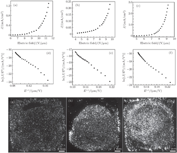
Fig. 3. (a)–(c) Field emission characteristics of patterned BNWs prepared on the different-width unit-cells at working distance 300 μm; (d)–(f) corresponding FN plots; (g)–(i) emission image of patterned BNWs prepared on the different-width unit-cells. The widths of unit cell are ((a), (d), and (g)) 100 μm, ((b), (e), and (h)) 150 μm, and ((c), (f), and (i)) 200 μm.

The relationship curves of patterned BNWs prepared on the different-width unit-cells between current density J and applied field E are shown in Fig. 3. From Figs. 3(a) and 3(b), the values of turn-on electric field Eto (at 10 μA/cm2) of different-width unit-cell B NWs patterned films are 7.1 V/ μm for 100 μm, 6.1 V/μm for 150 μm, and 5.4 V/μm for 200 μm, respectively. The values of threshold electric field (Ethr) (at 1 mA/cm2) with different-width unit-cell patterns are 11.2 V/μm for 100 μm and 8.4 V/μm for 200 μm, respectively. Comparing the unit size of 100 μm with that of 150 μm, the width of unit-cell of emitter with 200 μm shows low turn-on and threshold field. The threshold field value of width of unit-cell of these BNWs patterned films is higher than those of patterned B nanocones (3.8 V/μm)[15] and B nanocones films (5.3 V/μm),[6] but it is lower than those of other reported nanostructures including patterned BNWs (24.0 V/μm),[7] AlN nanowires pattern (13.1 V/μm),[11] and In2O3 nanowires arrays (17.7 V/μm).[17] These results demonstrate that the patterned 1D nanostructure could reduce screen effects and improve FE properties.

The Fowler–Nordheim (FN) curves of patterned BNWs prepared on the different-width unit-cell are plotted in Figs. 3(d)3(f). The FN plots of all samples show quasilinear relationships. The quasilinearity of the curves implies that Fowler–Nordheim theory for semiconductors is applicable here. These results are consistent with our previous reports about boron nanowires.[18]

In order to evaluate the uniformity of field emission for each sample, we measure their brightness distribution. Figures 3(g)3(i) show the emission images of the three samples, revealing clearly that they show different brightness in the emission process. When the width of unit-cell is 200 μm, the patterned BNWs have uniform emission brightness, indicating that the distribution of BNWs in each emitter unit is very uniform in this pattern. On the other hand, the emission brightness is nonuniform in each emitter unit when the width of unit-cell is 100 μm or 150 μm. From Figs. 3(h) and 3(i), it can be found that some center cells and edge cells have no emission. These results further indicate that a high turn-on field appears in unit-cell sizes of 100 μm and 150 μm.

In order to reduce the screening effect of boron nanowires, we prepare the boron nanowires (BNWs) by using different-width unit-cells. The widths and the numbers of the unit cells for these three Mo templates are quite different as summarized in Table 2. Therefore, the numbers and areas of the BNWs are very different when we use Mo masks with different-width unit-cells. As seen in Table 2, the structure parameters of three BNW patterns using different Mo masks are compared to better understand the originations of different FE behaviors.

The BNW sample using Mo mask with a 200-μm-wide unit-cell has the largest number of emitters on the Si substrate with the same area, which leads to the fact that it has the lowest turn-on and threshold field. It can be illustrated as follows. From Table 2, it can be found that the total area of the BNW patterns will increase from 0.1932 cm2 to 0.2864 cm2 when the width of unit-cell on Mo mask turns larger. Moreover, it is obviously seen that the growth density (1.0 × 10¹³/cm2) of the BNWs using the Mo mask with a 200-μm-wide unit-cell is nearly 4.2 times bigger than that (2.4 × 10¹²/cm2) of the BNWs using the Mo mask with a 100-μm-wide unit-cell on a pattern. So the BNW patterns using the Mo mask with the biggest-width unit-cell (200 μm) have the largest number (9.3 × 10⁸) of the nanowires on Si substrate in these three samples, which is almost 6.2 times bigger than that of the BNW patterns (9.3 × 10⁸) using the Mo mask with the smallest-width unit-cell (100 μm). It is suggested that the BNW sample using the Mo mask with a 200-μm-wide unit-cell has the largest number of the emitters on the Si substrate with the same area, and thus it should have the lowest turn-on and threshold field as seen in experiments.

Table 2.

Comparisons of structure parameters among three BNW patterns using Mo masks with different-width unit-cells.

.

Figure 4 shows the SEM images of BNWs prepared on different-deposition-width unit-cells. From this figure it can be seen that the uniformity of nanowire morphology in each pattern will turn higher with the increase of the unit-cell size on Mo mask. It also follows that the BNW patterns using a largest-width unit-cell (200 μm) have the lowest turn-on and threshold field. It can be explained in the following. The aspect ratio of the nanowires will increase with increasing the width of unit-cell of the Mo mask, which reveals that the BNW sample using the Mo mask with the largest-width unit-cell (200 μm) should have the highest field emission enhancement factor. Therefore, the actual number of the cathode emitters involved in field emission will correspondingly turn smaller if the nanowire uniformity is worse. Combining the morphology uniformity, the nanowire numbers of Si substrate, the aspect ratio of the nanowires, we can draw a conclusion that the turn-on and threshold field of the BNW patterns with better uniformity and higher aspect ratio will become lower. In other words, the BNW sample using the Mo mask with a 200-μm-wide unit-cell should have the best field emission properties, which is in good agreement with our measurement results.

Now a question arises: why can the 100-μm-wide unit cell not produce such a good aspect ratio nor uniformity like the 200-μm unit cell. The reason of uniformity and aspect ratio of nanowires affected by the unit-cell size can be derived from the preparation process of the patterned catalysts. In experiment, we use Fe3O4 nanoparticles (NPs) hexane solution to drop on the surface of the Mo mask to pattern the catalyst NPs. In this process, the soakage between the hollow region of the Mo mask and the catalyst NPs solution is insufficient due to the effect of the surface tensile force in the small space sizes of 100 μm and 150 μm unit. It might result in non-uniform distribution of NPs catalysts after removing the hexane solvent. Some parts of the surface of unit-cell are not covered by catalyst NPs. The concentrations of catalyst NPs decrease in the 100 μm and 150 μm unit. Therefore, they affect the growth of nanowires, which leads to the relative non-uniformity and reduction of length of nanowires (Figs. 4(a) and 4(b)).

Fig. 4. SEM images of BNWs prepared on unit-cells with widths of (a) 100 μm, (b) 150 μm, and (c) 200 μm.
4. Conclusions

Large-area films of boron nanowires (BNWs) patterned with different-width unit-cells (100, 150, and 200 μm) are fabricated using the Mo mask as templates by the chemical vapor deposition (CVD) method. The BNWs have an average diameter of about 20 nm and lengths of 10 μm–20 μm. The high-resolution transmission electron microscopy and select area electron diffraction results show that the boron nanocones have a β-tetragonal structure with good crystallization. Field emission measurements of BNW films patterned with different-width unit-cells show that their turn-on and threshold electric field decrease with increasing the width of unit-cell. The results indicate that the patterned growth method is also applicable to optimizing the FE properties of other field emitter nanostructures.

Reference
1Tian J FXu Z. CShen C MLiu FXu N SGao H J 2010 Nanoscale 2 1375
2Xu N SHuq S E 2005 Mater. Sci. Eng. 47 R48
3Tsagareishvili G VTavadze F N 1988 Prog. Crystal Growth Charact. 16 341
4Wang D WLu JOtten C JBuhro W E 2003 Appl. Phys. Lett. 83 22
5Zhang Y JAgo HYumura MKomatsu TOhshima SUchida KIijima S2002Chem. Commun.232806
6Wang X JTian J FYang T ZBao L HHui CShen C MGao H J 2007 Adv. Mater. 19 4480
7Li C.Tian YWang D KShi X ZHui CShen C MGao H J 2011 Chin. Phys. 20 037903
8Menz WMohr JPaul O2001Microsystem Technology2nd edn.WeinheimWiley-VCH
9Geissler MXia Y 2004 Adv. Mater. 16 1249
10De Heer W AChâtelain AUgarte D 1995 Science 270 1179
11Liu NWu QHe C YTao H SWang X ZLei WHu Z 2009 ACS Appl. Mater. Interfaces 1 1927
12Tang Y BCong H TChen Z GCheng H M 2005 Appl. Phys. Lett. 86 233104
13XiaoWuBai XZhang WYu L G 2008 J. Phys. D: Appl. Phys. 41 135409
14Liu FTian J FBao L HYang T ZShen C MXu N SGao H J 2008 Adv. Mater. 20 2609
15Li CTian YHui CTian J FBao L HShen C MGao H J 2010 Nanotechnology 21 325705
16JCPDS-International Center for Diffraction Data, PCPDFWIN, v.2.1, 2000
17Li QLiang Y XWang T H 2006 Appl. Phys. Lett. 88 053107
18Tian YShen C MLi CShi X ZHuang YGao H J 2011 Nano Research 4 780