Preparation of patterned boron nanowire films with different widths of unit-cell and their field emission properties
Zhang Yong-Xin1, Liu Fei2, Shen Cheng-Min1, †,  , Li Jun1, Deng Shao-Zhi2, Xu Ning-Sheng2, Gao Hong-Jun1, ‡,
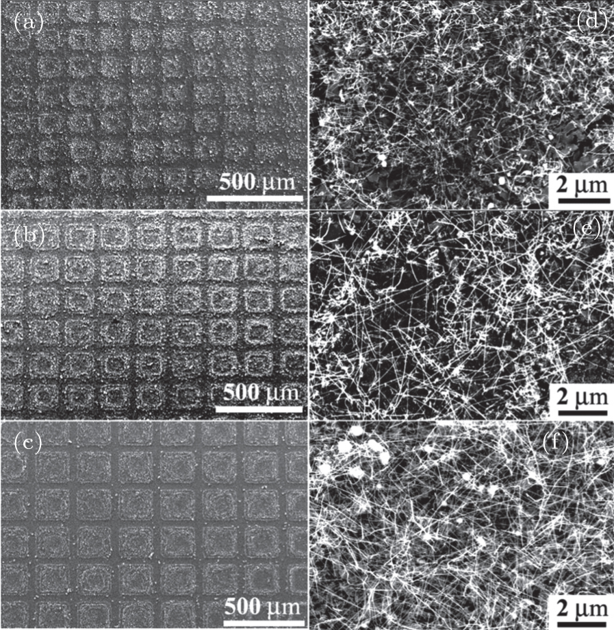
, Li Jun1, Deng Shao-Zhi2, Xu Ning-Sheng2, Gao Hong-Jun1, ‡, SEM images of ((a)–(c)) large-area patterned boron nanowires prepared on the unit-cells with different widths. (d)–(f) High-magnification SEM images of the same boron nanowire patterns. The widths of the unit-cells are ((a) and (d)) 100 μm, ((b) and (e)) 150 μm, and ((c) and (f)) 200 μm.