Preparation of patterned boron nanowire films with different widths of unit-cell and their field emission properties
Zhang Yong-Xin1, Liu Fei2, Shen Cheng-Min1, †,  , Li Jun1, Deng Shao-Zhi2, Xu Ning-Sheng2, Gao Hong-Jun1, ‡,
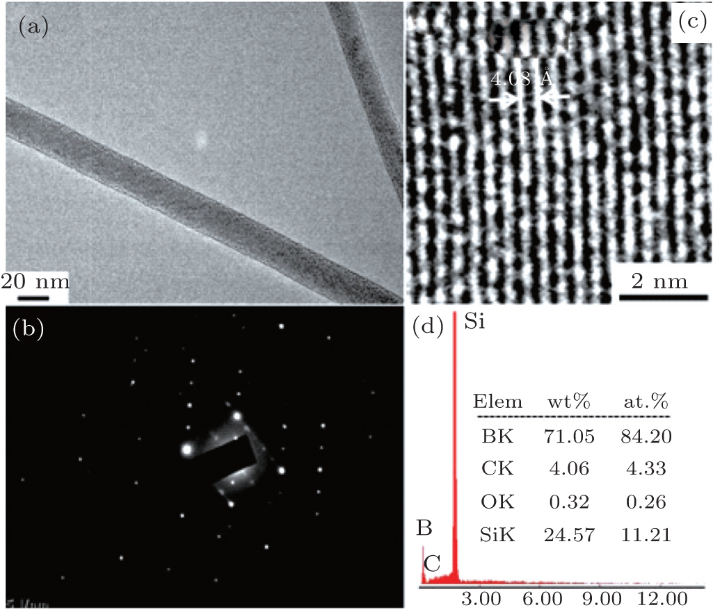
, Li Jun1, Deng Shao-Zhi2, Xu Ning-Sheng2, Gao Hong-Jun1, ‡, Morphology and structure of boron nanowires. (a) TEM image of an individual boron nanowire; (b) SAED pattern and (c) HRTEM image, indicating single crystal with a