1. IntroductionGraphene has attracted significant attention as a potential emerging semiconductor material for future electronics due to its excellent physical and electrical properties, such as the outstanding carrier mobility, high current density, large mechanical strength, excellent thermal conductivity, etc.[1–3] Over the past ten years, a number of advances in graphene based devices have been made. A intrinsic cutoff frequency (fT) of 427 GHz with 67-nm gate length graphene field-effect transistor (GFET) has been reported for peeled graphene.[4] Recently, 100-nm gate length epitaxial graphene transistor fabricated on SiC substrate has exhibited an intrinsic fmax of 137 GHz.[5] Several other significant efforts have also been made to improve the device performance and develop new graphene-based applications,[6–9] such as graphene nanoribbons, terahertz devices, photodetectors, and other graphene-based devices and circuits. In practical applications, however, graphene devices demand not only good operation performances but also thermal stabilities. Thermal effects, including self-heating generated during device operation and ambient temperature variations, will strongly affect the characteristics of devices, leading to degradations of device performances. Therefore it is very important to understand the operation mechanisms of graphene devices at different temperatures.
Many groups have reported on the temperature dependent characteristics of graphene devices at relatively low temperatures, typically ranging from ∼1.5 K to 380 K.[10–12] For example, Bolotin et al. investigated the temperature-dependent transport in suspended graphene in a temperature range 5 K < T < 240 K.[11] Feng et al. studied the temperature-dependent electrical properties of GFETs in ambient atmosphere with temperature rising from 300 K to 380 K.[12] These early studies gave an insight into the understanding of the basic physical and electronic properties of graphene. In many practical applications, devices often work under different kinds of high temperature conditions, such as the temperature above 100 °C. It is important to investigate the behaviors of graphene devices under high temperature. But few reports on high temperature performances of graphene devices can be found in the literature.
In this work, bilayer epitaxial GFETs are fabricated on 4H–SiC substrate. The DC performances of graphene devices are studied at the temperatures ranging from 25 °C to 200 °C. The operation mechanisms and thermal stabilities of GFETs under high temperature are investigated.
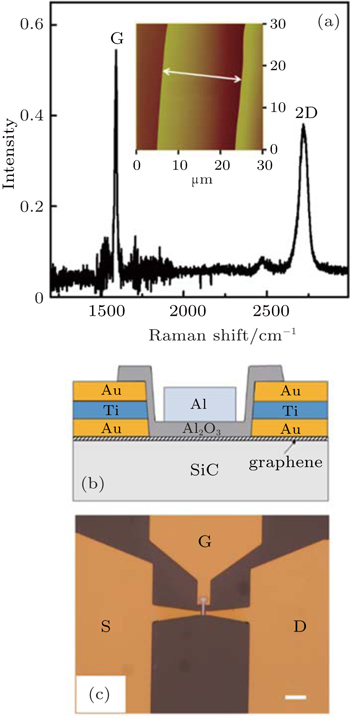
3. Results and discussionRaman spectrum of bilayer epitaxial graphene on SiC substrate is shown in Fig. 1(a). The full width of half maximum (FWHM) of two-dimensional (2D) peak is ∼59 cm−1, and the 2D band can be divided into four Lorentzian sub-bands, which is the evidence for bilayer structure of graphene.[17] An inset of Fig. 1(a) shows the morphology of graphene surface characterized by atomic force microscopy (AFM), revealing smooth and wide terrace which is around 19 μm. Figure 1(b) shows a schematic diagram of top-gated GFET on SiC substrate. The device structure consists of a graphene channel that is gated through Al2O3 dielectric from the top gate. Optical microscope image of GFET is shown in Fig. 1(c) with a gate length (Lg) of 1.2 μm and a gate width (Wg) of 2 μm.
Figures 2(a) and 2(b) show the variations of drain-source current (IDS) with drain-source voltage (VDS) scanned from 0 to −2 V for gate biases (VG) ranging from −8 V to +8 V at different temperatures (from 25 °C to 200 °C in steps of 25 °C). The bilayer graphene device shows p-type characteristic. The maximum IDS (defined at VDS = − 2 V and VG = −8 V) decreases with increasing temperature and drops from 2.36 A/mm to 2.07 A/mm as temperature increases from 25 °C to 200 °C. When increasing the VG to +8 V, the IDS shows a weak temperature dependence, and the minimum IDS (VDS = − 2 V, VG = +8 V) shows no obvious change with temperature. Figure 2(c) shows the curves of transfer characteristics and gm at VDS = − 2 V with VG scanned from −8 V to +8 V at various temperatures. Both IDS and gm decrease with increasing temperature, indicating degeneration of device performance under high temperature environment. It is seen that at the VG of −8 V, IDS decreases obviously with the increase of temperature, but has little change at the VG of +8 V (near the charge neutrality point), which is similar to the phenomenon as mentioned above in curves of IDS–VDS. To investigate the temperature-dependent IDS of GFET over different values of VG, the variations of IDS are quantitatively calculated as shown in Fig. 2(d). The value of variation in IDS is defined as θ = ((IDS − 25 °C − IDS−200°C)/IDS−25 °C) × 100%. At the VG of −8 V, a reduction of 12.58% is observed from 25 °C to 200 °C, while at the VG of +8 V, the reduction is only as small as 0.88%. A similar phenomenon has been seen in several theoretical and experimental studies.[11,18,19] An inset in Fig. 2(d) shows the energy-band diagram of graphene with VG swept from −8 V to +8 V. For graphene at high carrier density, the temperature-dependent scattering effect becomes prevailed, which leads to a metallic behavior (∂σ/∂T < 0, σ = neμ) of the graphene channel conductance. While in a low carrier density region (at or close to the Dirac point), thermal activation of charge carriers in electron-hole puddles originating from potential fluctuations associated with randomly distributed charged impurities plays a very important role, which gives rise to the increase of carrier density and results in a semiconducting behavior (∂σ/∂T > 0).
For our device, when VG = −8 V, a high carrier density regime is formed in the channel of graphene. Thermal activation of electron-hole puddles is exponentially suppressed at this time, and the scattering effect plays a major role and dominates the channel of graphene. Hence the IDS (σ·E) of GFET decreases obviously with increasing temperature, and 12.58% reduction of IDS is observed under 200 °C with VG = −8 V. The gate voltage is scanned from negative to positive voltage, and the number of carriers in the channel is reduced, and IDS shows a continuous drop with VG increasing. At a VG of +8 V, a relatively low carrier density regime is formed in the graphene channel and the thermal activation will dominate. It is needed to point out that to avoid the electrical breakdown of Al2O3 dielectric the bias applied to the gate does not exceed +8 V. The Dirac point is not reached in this measurement for our device. Dirac point is larger than +8 V, implying that the carrier density under VG of +8 V is not low enough and a pure semiconducting behavior cannot be present here. It is observed in Fig. 2(d) that the IDS shows a small reduction of 0.88% under a VG of +8 V at a temperature of 200 °C. The reduction indicates that a weak metallic behavior is still maintained in the graphene channel. This phenomenon is the result of the competing interactions between physical mechanisms of scattering and thermal activation, indicating that scattering has a stronger influence on the carrier of graphene than the thermal activation. Hence, only a little reduction of IDS is observed under the condition of VG = +8 V in the device.
It is important to note that the maximum IDS of GFET is only reduced by 12.58% after the temperature increasing from 25 °C to 200 °C. This value of reduction in the GFET is significantly smaller than those of other traditional semiconductors (e.g., silicon, GaN, etc.) devices. It is reported that a very large reduction of about 61% for the maximum IDS is observed in GaN-based MOSFET after the temperature rising from 25 °C to 200 °C.[20] To give an insight into the reasons for this small IDS reduction, the temperature-dependent scattering effect is used to investigate the operation mechanisms of GFETs. IDS can be determined using the following expression:

where
σ is the conductance of graphene channel,
E is the electric field between drain-source electrodes,
ns is the carrier density,
e is the charge of electron, and
μ is the carrier mobility. For a fixed
VDS,
IDS is proportional to the product of
ns and
μ. In our previous study, the carrier density
ns of bilayer QFSEG from Hall measurements (from 1.26 × 10
13 cm
−2 of 300 K to 1.28 × 10
13 cm
−2 of 500 K) showed a very slightly increase with temperature.
[14] The
ns can be regarded as a constant which is independent of temperature. Then,
IDS can be described by a simplified formula as
IDS =
A1·
μT, where
A1 is the fitting parameter and
μT is the mobility at different temperatures. It is well known that the carrier mobility is inextricably linked to the scattering. Here, four different scattering sources are considered: 1)
μc, Coulomb scattering; 2)
μgr, acoustic phonon scattering of graphene; 3)
μRP, remote optical phonon scattering from SiC substrate and gate dielectric of Al
2O
3; 4)
μsr, short range scattering, which can be approximately calculated by the following formulas for bilayer graphene, respectively:
[13,14]
where
A and
B are constants,
T is the temperature, and
nimp is the impurity density;

where
h is the reduced Planck’s constant,
ρs is the mass density of graphene (7.6 × 10
−7 kg·m
−2),
νs is the LA phonon velocity (2.1 × 10
4 m·s
−1),
VF is the Fermi velocity (∼ 1 × 10
6 m·s
1),
DA is the experimentally obtained deformation potential (18 eV), and
kB is the Boltzmann’s constant;
where
CRP−SiC and
CRP−Al2O3 are the coupling strength
Eop is the phonon energy coupled to the charge carriers in graphene, the values of
Eop−SiC,
Eop1−Al2O3, and
Eop2−Al2O3 are 116 meV, 55.01 meV, and 94.29 meV, respectively;
[21]

where
S is a constant. The total carrier mobility
μ can be regarded as the result of interaction among the four different scattering sources and is given by

The temperature dependences of the four kinds of scatterings are different. The strength of short range scattering depends on the quality of the graphene sample. The μsr is a constant and temperature independent. The μc shows a proportional relationship with temperature. Owing to the parabolic band structure of the bilayer graphene, the energy averaging of the Coulomb scattering time can result in the mobility increasing proportionally with temperature. The acoustic phonon scattering of graphene is inversely proportional to temperature, which results in the mobility decreasing with temperature. The carrier in the graphene will also be scattered by optical phonons of SiC substrates and Al2O3 dielectric, which results in the mobility decreasing with temperature. The competition result between Coulomb scattering and acoustic phonon scattering of graphene, and the remote phonon (RP) scattering of substrates/dielectric cause a relatively small decrease of μ at high temperature, which leads to the slight reduction of IDS in the GFETs. The above analysis indicates that the small decrease of μ at high temperature lies in the increase of Coulomb scattering mobility with temperature rising due to its parabolic band structure of bilayer graphene. The bilayer graphene transistors show some advantages in high temperature applications.
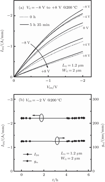
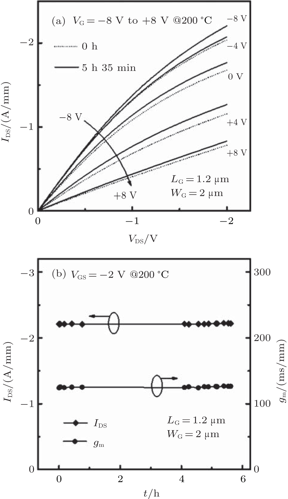
In order to further investigate the performance of GFET under high temperature, the thermal stability test is conducted in this work. The measurement is carried out under 200 °C in air ambience. The output characteristics of a GFET at different heating times are shown in Fig. 3(a). It is observed that the graphene device exhibits almost unchanged performance after high temperature measurements at 200 °C for 5 hours. Figure 3(b) shows the results of the maximal IDS and gm versus time, demonstrating a long-term thermal stability for bilayer graphene device.


 , Cai Shu-Jun2]