1. IntroductionNumerous technological and scientific challenges have to be surmounted to continue Moore’s law, which predicts that the device density will double every 18 to 24 months. The aggressive scaling of silicon (Si) electronics that comes along with the scaling of the silicon dioxide (SiO2) based gate dielectrics leads to unacceptable high gate leakage currents due to direct tunneling.[1,2] With the development of the microelectronics industry, numbers of high-k materials have been investigated as candidates to replace SiO2 as the gate dielectrics.[3] Candidate materials include Al2O3,[4] La2O3,[5] HfO2,[6] and Nd2O3,[7] La2O3 is an attractive gate dielectric candidate for replacement of SiO2 in further scaled metal–oxide–semiconductor field effect transistors (MOSFETs) due to several advantages such as a higher permittivity (∼ 27), a larger conduction band off-set (∼ 2.3 eV), and good thermodynamic stability with Si.[8] However, La2O3 is so moisture sensitive that it is considered to be incompatible with large-scale integration processes. La2O3 can easily form both La-silicate and La-hydroxide because of the catalytic and hygroscopic behavior. It will cause the decrease of the dielectric constant and the performance degradation of the films.[3] Al2O3 has many favorable properties like kinetic stability and thermodynamic stability on Si up to high temperatures, good interface with Si, and low bulk defect density.[9] However, the dielectric constant of Al2O3 (6.5–9) is low. Lanthanum aluminate (LaAlO3), which is a compound of La2O3 with a high dielectric constant and Al2O3 with a large band gap, has high immunity against ambient moisture while offering both comparable thermal stability on Si and high dielectric constant (25–27). Therefore, LaAlO3 is regarded as a promising candidate for high-k gate dielectrics.[10]
Uniform and conformal thin films have a wide variety of applications in semiconductor microelectronics. It is necessary to use a deposition technique that can produce films with good dielectric properties, accurate thickness, and smooth surface.[11] One method that is particularly suitable for making uniform and conformal layers is atomic layer deposition (ALD). ALD is a process for depositing highly uniform and conformal thin films by alternating exposures of a surface to vapors of two chemical reactants. By contrast with metal-organic chemical vapor deposition (MOCVD), molecular beam epitaxy (MBE), and pulsed laser deposition (PLD), ALD is based on self-limiting film growth via alternate saturative surface reaction. Therefore, the films deposited by ALD have high density, high purity, and accurate thickness. In this study, we investigate the LaxAlyO nanolaminate films with different structures and different oxidants deposited on Si substrates by ALD, which is an attempt to ensure the uniformity and conformity of the films. The electrical characteristics and physical properties of the films with different oxidants (H2O and O3) and different structures are studied and compared.
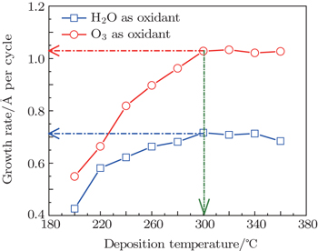
3. Results and discussionThe deposition temperature of ALD should be in the range where the surface-limited reaction occurs with a constant growth rate. Each film has an optimum temperature for the growth. Figure 1 shows the temperature dependence of the La2O3 growth rate when the process temperature is varied from 200 °C to 360 °C. The curves with red and blue colors stand for the growth rates of La2O3 films when O3 and H2O are used as the oxidant, respectively. When H2O is used as the oxidant, the growth rate of La2O3 increases as the temperature increases, and maintains a stable value (0.65–0.7 Å/cycle) when the temperature is above 260 °C. When O3 is used as the oxidant, the growth rate of La2O3 acquires a certain value when the deposition temperature is above 300 °C. A stable growth rate of 1 Å/cycle is obtained in the temperature range of 300–360 °C. Therefore, the temperature ranges of 260–360 °C and 300–360 °C within which the surface-limited reaction would most probably occur are set to investigate the influence of the deposition temperature on the growth rate when H2O and O3 are used as the oxidant, respectively.[7] When H2O and O3 are used as the oxidant, the growth rates of Al2O3 films measured by the spectroscopic ellipsometry are 0.97 Å/cycle and 1.04 Å/cycle, respectively. Therefore, 300 °C is selected as the ALD deposition temperature for LaxAlyO films. At this temperature, when H2O and O3 are used as the oxidant, the growth rates of La2O3 films are 0.71 Å/cycle and 1.03 Å/cycle, respectively.
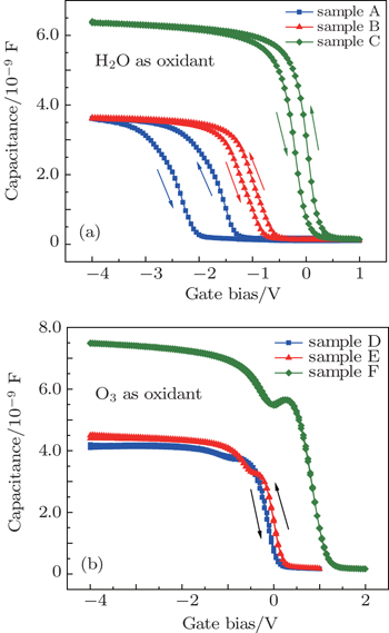
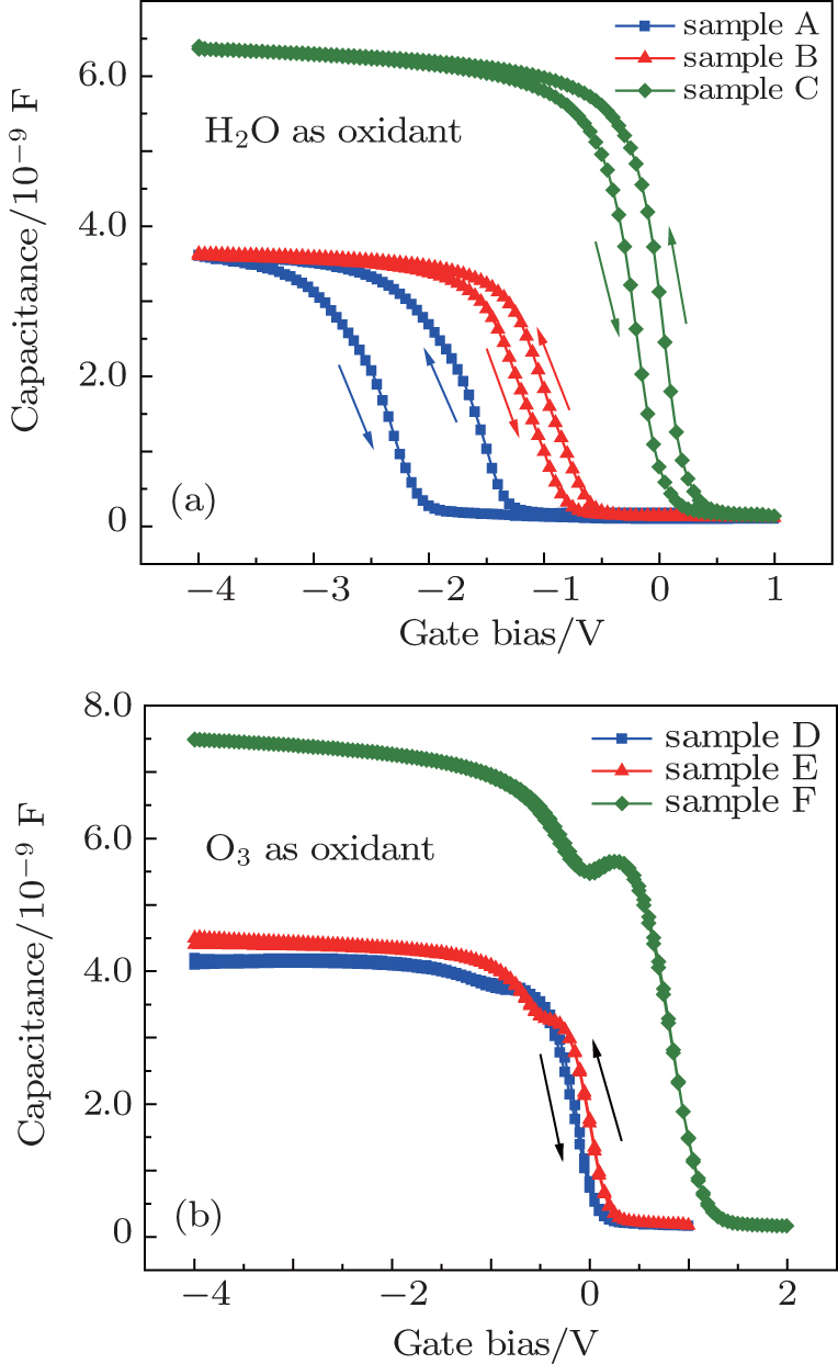
Figure 2 shows the C–V characteristics of the LaxAlyO films with different structures and different oxidants. The gate voltage is swept from negative to positive and then back to negative. In Fig. 2(a), the hysteresis voltage of sample A is 752 mV. The relatively large anticlockwise hysteresis loop during forward and reversed bias sweeps indicates serious charge trapping in the oxide. This could be attributed to the formation of a defective LaAlSiOx, LaSiOx, and AlSiOx interface layer and Si out diffusion during the ALD process, causing the poor interface quality and large interface state density.[12,13] In contrast, samples B and C possess smaller hysteresis voltages, which are 205 mV and 221 mV, respectively. To a certain extent, in samples B and C, the barrier layers of SiO2 and Al2O3 can retard the interdiffusion of Si, Al, La, and O atoms. The interface layer of sample B is attributed to the formation of LaAlSiOx, LaSiOx, and AlSiOx. The interface layer of sample C is attributed to the formation of AlSiOx. Because of the favorable property of the good interface of the Al2O3 film with silicon, which can reduce the diffusion of La and Si atoms and the formation of La-silicate, compared to sample A, samples B and C possess better interface quality and smaller interface state density. Moreover, the accumulation capacitance increases with the change of the type of the structure; this is attributed to a decrease of the concentration of the interfacial fixed charge and defects.[14] Table 2 shows the physical thickness, flat band voltage (VFB), equivalent oxide thickness (EOT), and dielectric constant of the films. The VFB of samples A and B are −1.37 V and −0.64 V, respectively. This is attributed to the formation of positive fixed charge in the films. The formation of oxygen vacancies in the LaxAlyO films increases the positive oxide charge due to the growth of a silicate interfacial layer (IL).[15–17] However, VFB of sample C is 0.33 V. The flat band voltage shifts toward the positive direction, which indicates the formation of negative charge in the film. This is attributed to the strong dipole bonding at the interface.[11]
Table 2.
Table 2.
 Table 2. Overview of characterization results of samples. .
| Sample |
Physical thickness/nm |
VFB/V |
EOT/nm |
k |
|---|
| A |
13.27 |
−1.37 |
5.55 |
9.32 |
| B |
15.43 |
−0.64 |
3.91 |
15.39 |
| C |
15.19 |
0.33 |
3.13 |
18.90 |
| D |
12.85 |
−0.21 |
4.76 |
10.52 |
| E |
14.33 |
0.16 |
2.94 |
19.04 |
| F |
14.27 |
1.16 |
2.67 |
20.83 |
| Table 2. Overview of characterization results of samples. . |
In Fig. 2(b), the C–V curves with O3 as the oxidant show a wide step, which is caused by the trapped holes injected from the LaxAlyO layer into the depletion layer. The width of the depletion layer in the Si substrate grows with the gate bias increasing. The growth of the depletion layer will stop and the capacitance becomes constant after all the trapped holes in the interface layer are injected into the depletion layer.[6] The hysteresis voltage of sample D is 20 mV, while the hysteresis voltages of samples E and F can be ignored. The negligible hysteresis voltages indicate the good interface quality and small interface state density in samples E and F. Moreover, the accumulation capacitance increases with the change of the type of the structure, this is attributed to a decrease of the concentration of the interfacial fixed charge and defects. Compared to the LaxAlyO films with H2O as the oxidant, the films with O3 as the oxidant possess larger accumulation capacitances, which is attributed to the small EOT and high dielectric constant. According to the previous report,[18] the La2O3 film can react with moisture easily and form La(OH)3 which will decrease the whole dielectric constant of the film. The extracted VFB of the LaxAlyO films in samples D, E, and F are shown in Table 2. The VFB of the three samples are −0.21 V, 0.16 V, and 1.16 V, respectively. These phenomena are attributed to the formation of positive fixed charge because of the formation of oxygen vacancies in sample D. The increase of the positive oxide charge is due to the interdiffusion of Si, Al, La, and O atoms, and the growth of the silicate interfacial layer is attributed to the formation of LaSiOx, AlSiOx, and LaAlSiOx.[19] Compared to the LaxAlyO films with H2O as the oxidant, the films with O3 as the oxidant possess smaller VFB. This indicates that the LaxAlyO films with O3 as the oxidant have smaller EOT and better quality interfacial layers.
The EOT and permittivity are determined as follows:


where
A is the area,
Cox is the accumulation capacitance of the films,
TSiO2 and
Thigh-k are the thicknesses of the native oxide and the deposited films,
εhigh-k is the permittivity of the La
xAl
yO films, and
ε0 and
εSiO2 are the permittivities of vacuum and SiO
2, respectively.
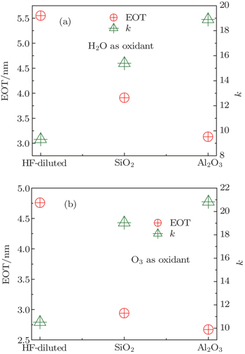
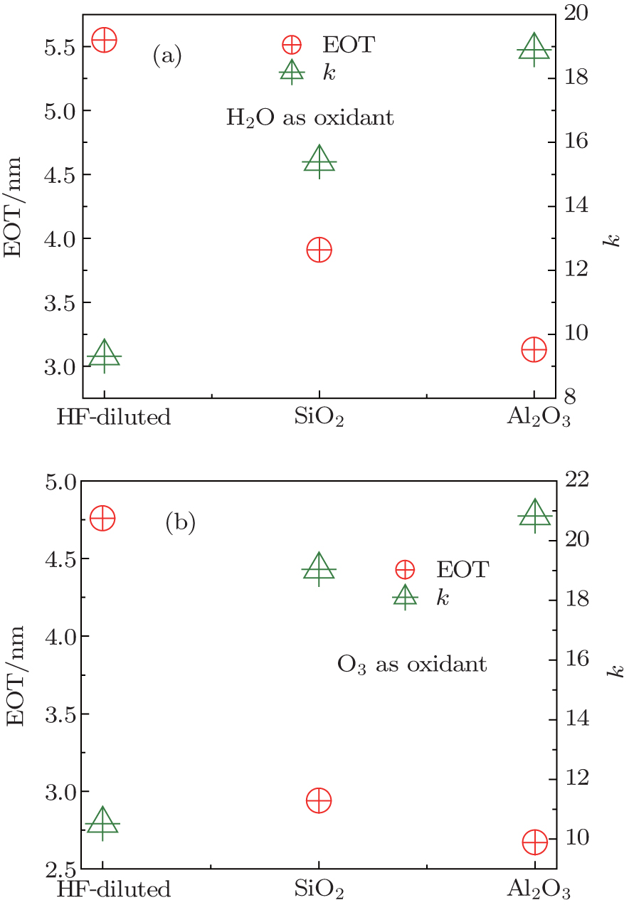
In Table 2, for the same structure, the physical thicknesses of samples A, B, and C are larger than those of samples D, E, and F. This is attributed to the formation of a thicker IL in the samples that H2O is used as the oxidant. The extracted dielectric constant and EOT of the samples are shown in Fig. 3. In Fig. 3(a), the EOT decreases and the dielectric constant increases by varying the type of the structure of the films. For sample A, the large EOT is attributed to the formation of LaSiOx, LaAlSiOx, and AlSiOx which is due to the interdiffusion of La, Al, O atoms from La2O3 and Al2O3 films close to the substrate and Si atoms from the Si substrate. On the other hand, the small dielectric constant is attributed to the formation of La(OH)3, which is mainly due to a moisture adsorption at the top surface of La2O3. For sample B, the EOT and the dielectric constant are 3.91 nm and 15.39, respectively. Similar to sample A, sample B has an interface layer of LaSiOx, LaAlSiOx, and AlSiOx.[20] However, because of the existence of the SiO2 layer, the interdiffusion of La, Al, O, and Si atoms are restrained. The formation of LaSiOx, LaAlSiOx, and AlSiOx is mainly due to the interdiffusion of La, Al, and O atoms and Si atoms from the SiO2 barrier layer. This leads to a smaller interface layer in sample B. Furthermore, for sample C, the EOT and the dielectric constant are 3.13 nm and 18.90, respectively. The smallest EOT is attributed to the Al2O3 layer which possesses a good interface with silicon and can restrain the diffusion of La and Al atoms into the Si substrate. Only a few AlSiOx are formed between the Al2O3 layer and the Si substrate.
The EOT and the dielectric constants of samples D, E, and F are 4.76 nm, 2.94 nm, 2.67 nm and 10.52, 19.04, 20.83, respectively, as shown in Fig. 3(b). For the same structure, the dielectric constants of the films with H2O as the oxidant are lower than those with O3 as the oxidant. This phenomenon is mainly attributed to the more La-hydroxide and La-silicate formed during the ALD process. The La2O3 films react with moisture from the H2O oxidant, carrier and purge gas and form La(OH)3. Moreover, the La-silicate also decreases the dielectric constants of the films. For the films with O3 as the oxidant, moisture only comes from the carrier, purge gas and less La-hydroxide is formed in the films. This explains why the films possess relative higher dielectric constants. However, the dielectric constants we obtained are smaller than the theoretical ones of the LaAlO3 films, this probably is due to the fact that the LaxAlyO films are preserved in air for a long time after deposition, which prohibit the La2O3 films from reacting to moisture in air and forming La-hydroxide.
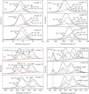
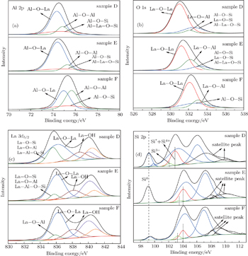
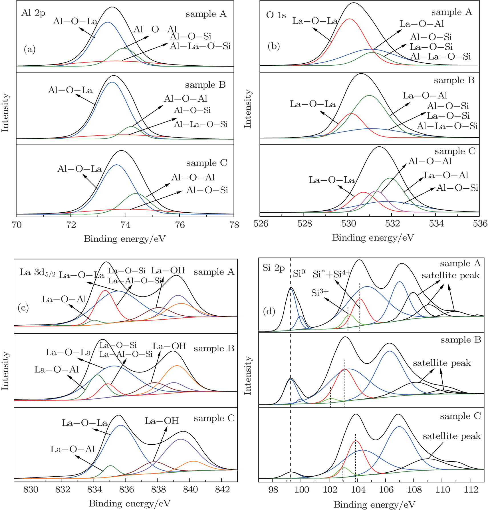
In order to confirm the above analyses, XPS spectra were obtained with using Al Kα. The binding energy (BE) was calibrated with the position of the C 1s peak at 284.8 eV. Figure 4 depicts the XPS Al 2p, La 3d5/2, O 1s, and Si 2p spectra of the LaxAlyO films with H2O as the oxidant. As shown in Fig. 4(a), the Al 2p spectrum is fitted with three peaks after the application of a smart background. Blue and green curves stand for the Al–O–La and Al–O–Al peaks, respectively.[21] The existence of Al–O–La and Al–O–Al bonds is attributed to the formation of LaxAlyO and Al2O3 in the films. The red curves stand for the aluminium compound formed in the films. The binding energy of aluminates in sample C is slightly higher than that in samples A and B; this indicates that the types of aluminium compound are different between sample C and the other two samples.[6] Sample A contains Al–O–Si and Al–La–O–Si bonds, which are attributed to the diffusion of La and Al atoms into the Si substrate. Similar to sample A, sample B also contains the Al–O–Si and Al–La–O–Si bonds. However, the Si atoms in these bonds come from the SiO2 barrier layer, while the Al–O–Si bonds in sample C are attributed to the reaction of the Al2O3 barrier layer with the Si substrate. On the other hand, the intensity of the Al–O–La peak of sample A is smaller than that of sample B; the intensity of aluminium compound peak of sample A is larger than that of sample B. Thus, sample B possesses a smaller EOT and a higher k than sample A. The O 1s spectra of samples A and B are fitted with three peaks after the application of a smart background, as shown in Fig. 4(b). Red, green, and blue curves stand for the La–O–La, La–O–Al, and La–Al–O–Si contributions, respectively.[12,20,22] The La–O–La bonds are attributed to the formation of La2O3 in the films during the ALD process. The pink curve of sample C stands for the Al–O–Al bonds of the Al2O3 barrier layer. The binding energy of the peak indicated by the blue curve for sample C is slightly higher than that for samples A and B; this indicates that the types of chemical compound in the IL are different between sample C and the other two samples. The XPS analyses of O 1s are in consonance with the analyses of Al 2p. Figure 4(c) shows the La 3d5/2 spectra of the samples. The La–Al–O, La–O–La, silicates, and La–OH bonds are indicated by green, blue, red, and brown curves, respectively.[12,23] The existence of La–OH peaks is attributed to the formation of La(OH)3 which is mainly due to the moisture adsorption of La2O3. The variation tendency of La–O–Al and silicates bonds of samples A and B in the La 3d5/2 XPS spectrum is in accordance with that in the Al 2p and O 1s XPS spectra. Figure 4(d) shows the Si 2p spectra of the samples. The binding energy located at 99.3 eV is the Si0 peak, which is attributed to the Si substrate.[24] The higher peaks indicated by black are satellite peaks. The green and red curves indicate Si3+ and Si* + Si4+, respectively, which come from the silicates and SiO2−x.[22,24] The shift of the peaks of the silicates indicates that the types of chemical bonds of silicates are different. For sample B, because of the existence of the SiO2 barrier layer, the amount of silicates in the sample is smaller than that in sample A. This causes the smaller EOT of sample B. On the other hand, the existence of Si* + Si4 + is attributed to the formation of SiO2 between the Si substrate and the Al2O3 barrier layer.
Figures 5(a)–5(d) show the XPS Al 2p, La 3d5/2, O 1s, and Si 2p spectra of the LaAlO3 films with O3 as the oxidant, respectively. The variation trends of the chemical bonds of Al 2p and O 1s of the films are similar to those of the films with H2O as the oxidant. However, in the La 3d5/2 spectra, the La–OH bonds are observed as shown in Fig. 5(c). The formation of La–OH bonds may be due to the reaction of moisture from air with La2O3 at the top of the LaAlO3 layer. The existence of La-hydroxide decreases the dielectric constants of the films. The intensity of Si* + Si4+ in the Si 2p spectrum decreases with the change of the type of the sample, and the film with Al2O3 barrier possesses smaller IL and EOT. All the XPS analyses are in accord with the analyses of electrical characteristics of the films discussed previously.


 , Wang Xing, Zhao Dong-Dong, Wang Shu-Long, Chen Shu-Peng]