


Temperature dependent direct-bandgap light emission and optical gain of Ge
Cite this Article
Liu Zhi, He Chao, Zhang Dongliang, Li Chuanbo, Xue Chunlai, Zuo Yuhua, Cheng Buwen. Temperature dependent direct-bandgap light emission and optical gain of Ge. Chinese Physics B, 2016, 25(5): 057804 
Permissions
Temperature dependent direct-bandgap light emission and optical gain of Ge
† Corresponding author. E-mail:
Project supported by the National Basic Research Development Program of China (Grant No. 2013CB632103) and the National Natural Science Foundation of China (Grant Nos. 61377045, 61435013, and 61176013).
Abstract
Abstract
Band structure, electron distribution, direct-bandgap light emission, and optical gain of tensile strained, n-doped Ge at different temperatures were calculated. We found that the heating effects not only increase the electron occupancy rate in the Γ valley of Ge by thermal excitation, but also reduce the energy difference between its Γ valley and L valley. However, the light emission enhancement of Ge induced by the heating effects is weakened with increasing tensile strain and n-doping concentration. This phenomenon could be explained by that Ge is more similar to a direct bandgap material under tensile strain and n-doping. The heating effects also increase the optical gain of tensile strained, n-doped Ge at low temperature, but decrease it at high temperature. At high temperature, the hole and electron distributions become more flat, which prevent obtaining higher optical gain. Meanwhile, the heating effects also increase the free-carrier absorption. Therefore, to obtain a higher net maximum gain, the tensile strained, n-doped Ge films on Si should balance the gain increased by the heating effects and the optical loss induced by the free-carrier absorption.
1. Introduction
Room-temperature Si-based light source is one of the most important components of Si-based photonic integration. In recent years, although many developments have been achieved for Si-based light emission,[1] to overcome the inefficient band-to-band radiative recombination of Si remains a challenge. In the last decade, due to the compatibility with CMOS processes, Ge on Si substrate has been widely studied for Si-based optoelectronic device applications.[2] Unlike Si, Ge has a direct bandgap only slightly larger (by 140 meV) than its indirect bandgap. The direct optical transition in Ge is a very fast process with a radiative recombination rate four orders of magnitude higher than that of the indirect transitions.[3] This pseudo-direct bandgap structure allows Ge to be a promising candidate for light emission. The key to improving Ge emitting is to increase electron occupancy in the Γ valley of the conduction band. There are several approaches to achieve this goal, such as tensile strain,[4,5] high n-doping,[6] and high injection.[7] Based on this principle, direct-gap transitions from Ge have been observed by photoluminescence,[6] electroluminescence,[7] optical gain,[8] and even by a Ge laser working at room temperature.[9,10] On the theoretical side, light emission and optical gain of Ge have been studied comprehensively by different models.[8,11,12] However, most theoretical studies concentrated on the light emission and optical gain of Ge under tensile strain and heavy n-doping at room temperature. The heating effects in Ge were ignored. Although light emission enhancement of Ge at high temperature was observed,[6,13,14] the temperature-dependent emission and optical gain of Ge have not been studied in detail.
In this work, we theoretically studied the band structure, electron distribution, direct-bandgap light emission, and optical gain of tensile strained, n-doped Ge at different temperatures. Our result indicated that the heating effects can increase the electron occupancy rate (Γ valley), light emission, and optical gain of Ge at a limited temperature range. We also discussed the free-carrier absorption (FCA) and net optical gain of tensile strained, n-doped Ge on Si.
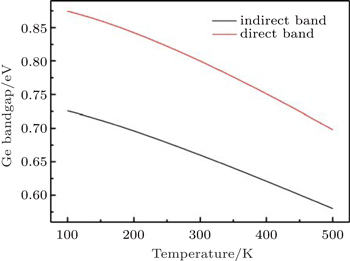
2. Temperature dependent band structure and electron distribution of Ge1 ), the calculation results of the indirect bandgap and direct bandgap of bulk Ge at different temperatures are shown in Fig. 1 . Like tensile strain, the heating effects not only shrink the bandgap of Ge, but also reduce the energy difference between the Γ valley and the L valley. The decrease of the energy difference between the Γ valley and the L valley has been proved to be an effective method to enhance the light emission of Ge.[4,5,16] Our results show that compared with bulk Ge at 300 K, the energy difference between the Γ valley and the L valley of bulk Ge reduces by 10 meV and 22 meV at 400 K and 500 K, respectively. For a thermal tensile strained Ge film, the thermal tensile strain reducing at high temperature should be considered.
The indirect bandgap and direct bandgap of Ge will both shrink with increasing temperature. Each bandgap has a different shrink rate. The temperature dependences of the indirect bandgap and direct bandgap of Ge are expressed as[15]

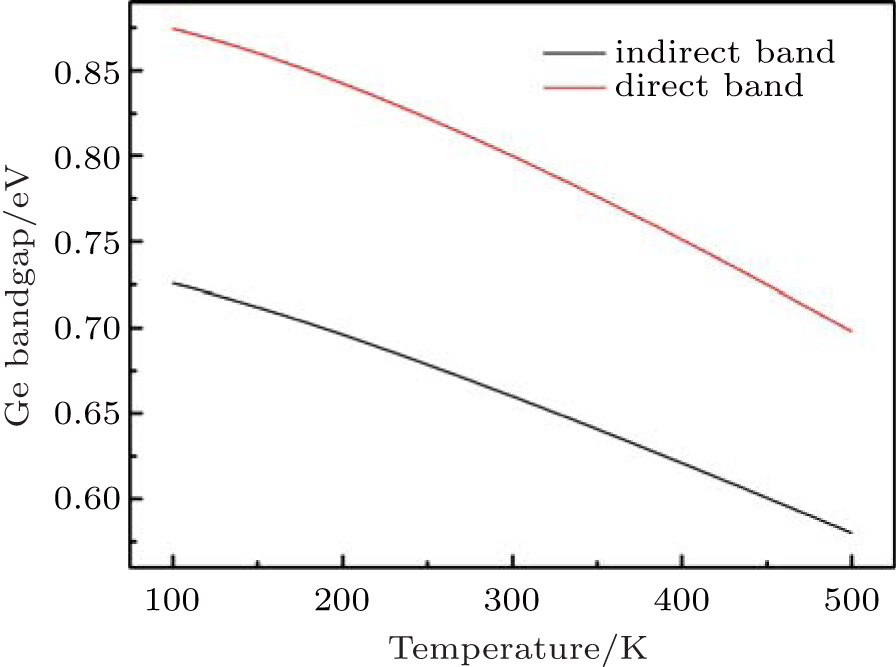 | Fig. 1. Indirect and direct bandgaps of bulk Ge at different temperatures. |
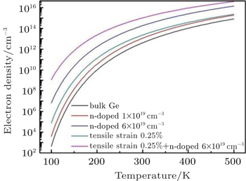
As the band structure of Ge is changed by the heating effects, the carrier distribution in the band is also changed. The electrons and the holes obey quasi-Fermi distributions with respect to the electron quasi-Fermi level (EFc) and the hole quasi-Fermi level (EFv). The occupation probabilities of an electron and a heavy hole are described by
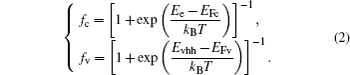
Unlike light emission from direct bandgap materials, the emission from Ge is interrelated only with the electron concentration in the Γ valley. According to Eq. (
 | Fig. 2. Electron densities in the Γ valley of different tensile strained, n-doped Ge samples at different temperatures. The input carrier concentration n = p = 1 × 1019 cm− 3. |
3. Temperature dependent light emission of Ge

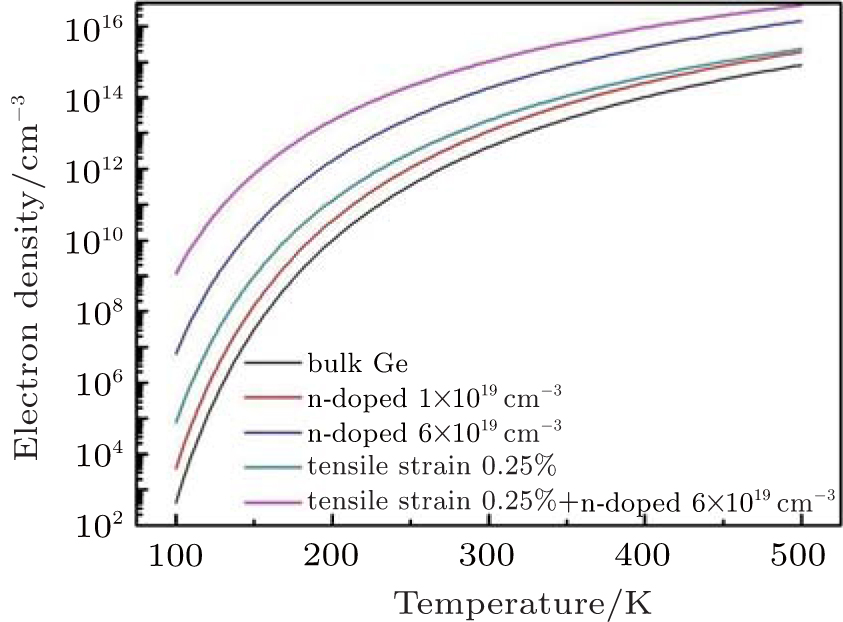
The emission of Ge is almost proportional to its spontaneous emission rate. Therefore, the total spontaneous emission intensity was used to study the emission intensity of Ge. For a given carrier concentration, the spontaneous emission rate of electrons in the Γ valley to the heavy hole band can be calculated according to the expression[18]


According to Eqs. (
 | Fig. 3. Light emission intensities of various n-doped Ge at different temperatures. The input carrier concentration n = p = 1 × 1019 cm−3. |
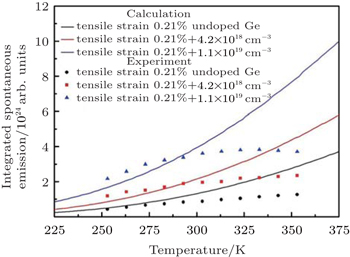
To verify the calculation results, temperature dependent photoluminescence measurements of three 0.21% tensile strain Ge films on Si with various n-doping (undoped, 4.2 × 1018 cm−3 n-doped, and 1.1 × 1019 cm−3 n-doped) were performed from 253 K to 353 K. The injected carrier density was estimated to be about 1 × 1019 cm−3. The experiment results and calculation results are shown in Fig.
 | Fig. 4. Temperature-dependent photoluminescence intensity and calculational light emission intensity of three 0.21% tensile strained n-doped Ge films on Si from 253 K to 353 K. The injected carrier density is estimated to be about 1 × 1019 cm−3. |
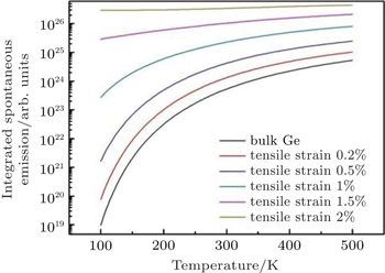
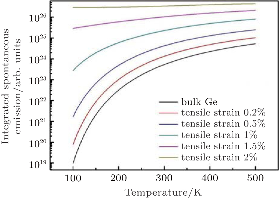 | Fig. 5. Light emission intensitits of various tensile strained Ge at different temperatures. The input carrier concentration n = p = 1 × 1019 cm−3. |
Figure
4. Temperature dependent optical gain of Ge
Although the electron occupancy rate in the Γ valley of Ge is low, the optical gain of Ge can be obtained in theory. The heavy n-doped Ge film on Si with 0.25% tensile strain is a typical example, which was used in optical gain and laser of Ge.[9,22] Therefore, we choose this typical example to study the optical gain of Ge at different temperatures. For a given carrier concentration, the gain spectrum of electrons in the Γ valley to the heavy hole band can be calculated according to the expression[18]


Figure
 | Fig. 6. Optical gain spectra of 0.25% tensile strained Ge films on Si with 6 × 1019 cm−3 n-doping at various temperatures. The input carrier concentration n = p = 1 × 1019 cm−3. |
When the temperature is lower than 300 K, the optical gain of 0.25% tensile strained Ge films on Si with 6 × 1019 cm−3 n-doping has positive temperature characteristics. This result can be explained by the fact that more electrons are thermally excited from the L valley to the Γ valley. When the temperature is higher than 300 K, the optical gain has the negative temperature characteristics, i.e., the optical gain decreases with the increase of the temperature. This phenomenon is attributed to the flatter hole distribution at high temperatures. The heating effects not only smear out the electron distribution and increase the electron occupation in the Γ valley, but also smear out the hole distribution, which prevents obtaining higher optical gain. This carrier distribution flattening is also reflected in the broadening of the gain spectral width. The gain spectral width increases from 125 nm at 200 K to 145 nm at 400 K.
To obtain the net optical gain of Ge, the optical loss induced by FCA should be considered, especially in high doping and high injection case. The FCA consisting of the absorptions of the L valley, the Γ valley, the heavy-hole band, and the light-hole band can be described by the Drude–Lorentz equation as follows:[21]
According to Eqs. (
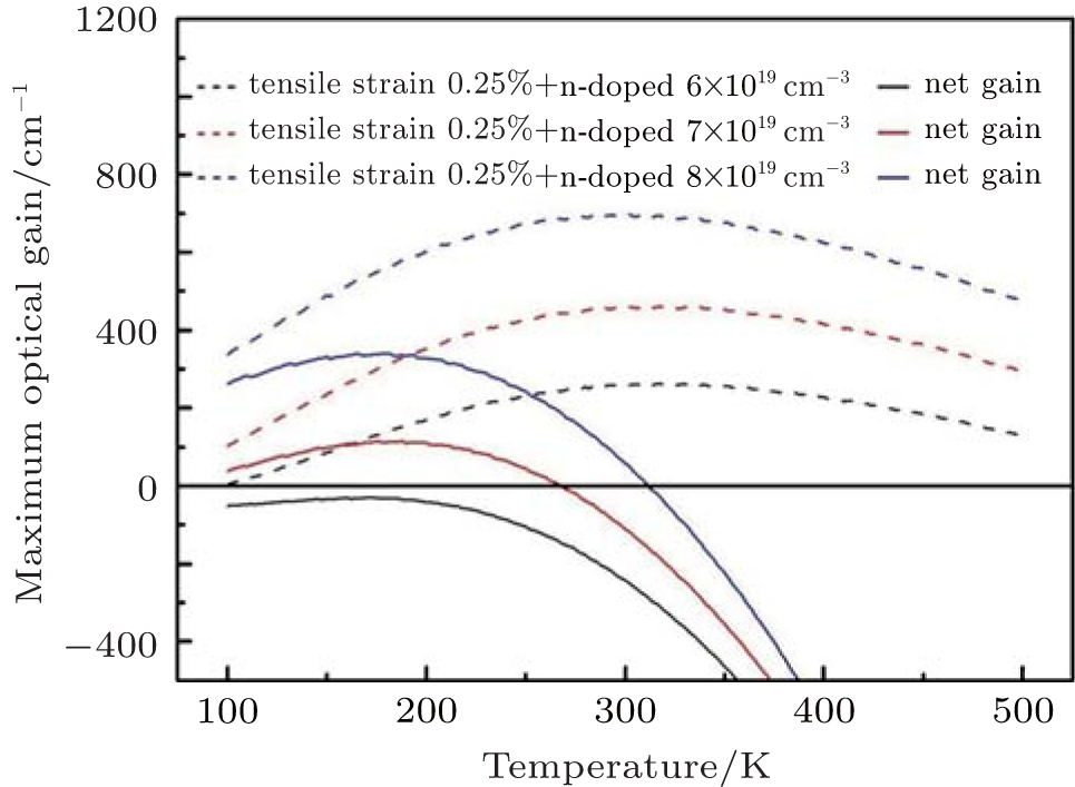 | Fig. 7. Maximum gain and net maximum gain of 0.25% tensile strained Ge films on Si with various n-doping at different temperatures. The input carrier concentration n = p = 1 × 1019 cm−3. |
5. Conclusion
We theoretically studied the band structure, electron distribution, direct-bandgap light emission, and optical gain of tensile strained, n-doped Ge at different temperatures. We found that the heating effects affect the light emission and optical gain of Ge in three aspects. Firstly, like tensile strain, the heating effects reduce the energy difference between the Γ valley and the L valley. This brings benefits to the light emission and optical gain of Ge. Secondly, the heating effects increase the electron occupancy rate in the Γ valley of Ge by Femi-level flattening (thermal excitation). The Femi-level flattening increases the light emission of Ge, but decreases the optical gain of Ge, when the hole and electron distributions become more flat at high temperatures. Thirdly, the heating effects increase the optical loss induced by FCA. Intensive FCA is one of the main reasons for the deterioration of the net optical gain of Ge at high temperatures. Therefore, to obtain high net maximum gain, tensile strained, n-doped Ge films on Si should balance the gain increase by the heating effect and the optical loss induced by the free-carrier absorption. This work helps to elucidate the mechanism of positive temperature characteristics of Ge light emission, and is useful for designing Ge light emitters and lasers.
Reference
| 1 | |
| 2 | |
| 3 | |
| 4 | |
| 5 | |
| 6 | |
| 7 | |
| 8 | |
| 9 | |
| 10 | |
| 11 | |
| 12 | |
| 13 | |
| 14 | |
| 15 | |
| 16 | |
| 17 | |
| 18 | |
| 19 | |
| 20 | |
| 21 | |
| 22 |