1. IntroductionThe super-junction (SJ) VDMOS has attracted a great deal of attention owing to its improvement on the specific on-resistance (Ron,sp) and the better trade-off between the Ron,sp and breakdown voltage (BV).[1–8] However, the Ron,sp is still determined by the doping concentration of the drift region. For high voltage SJ VDMOS, narrowing the width of the pillars is a good choice to improve the Nn and reduce the Ron,sp, but the fabrication is hard to realize. A vertical extended gate is used to form a major accumulation layer, thus reducing the Ron,sp.[9,10] Nevertheless, the peak electric field at the bottom of the extended gate causes a premature breakdown, thus limiting the BV. In Refs. [11] and [12], a gradient oxide layer between the extended gate and drift is adopted to modulate the drift electric field distribution. The BV is thus improved to some extent. Unfortunately, the peak electric field still limits the application scope below 200 V and the gradient oxide layer is fairly difficult to fabricate.
In this paper, a novel high voltage ultra-low Ron,sp VDMOS with continuous electron accumulation layer is proposed. It is characterized by an extended gate and two PN junctions in series within the extended gate. Owing to the electron accumulation layer in the on-state, the Ron,sp is reduced dramatically and almost independent of n-pillar doping concentration. Furthermore, the two PN junctions within the trench gate support a high gate-drain voltage in the off-state and on-state, respectively. The 800 V-class BV is obtained. It not only breaks through the silicon limit of conventional VDMOS, but also shows superiority to the trench gate SJ VDMOS.
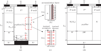
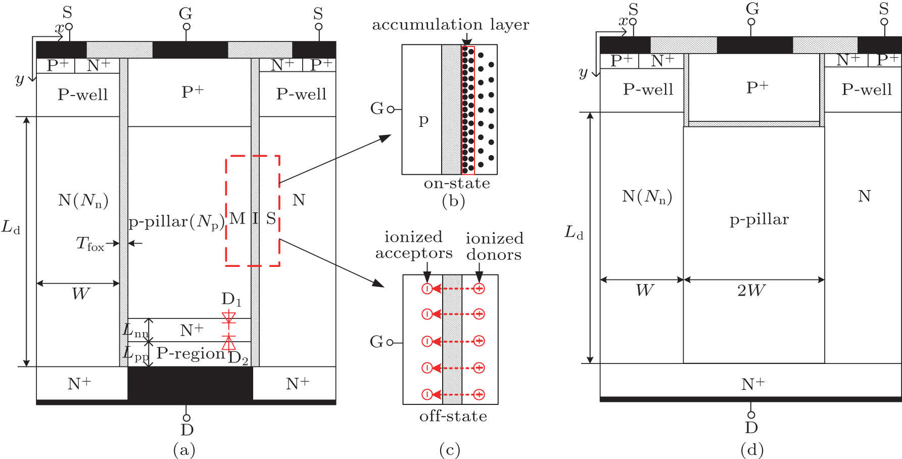
2. Device structure and mechanismFigure 1 shows the structures and operation mechanisms of the CEA-VDMOS and CSJ-VDMOS. As figure 1(a) shows, the trench gate extends to the drain and includes two PN junctions. In the extended gate, the p-pillar is in touch with the P+ gate contact region at the top. The P-region is contacted with the drain electrode at the bottom. The N+ region is between the p-pillar and the P-region. Therefore, the D1 and D2 junctions are formed. The D1 and D2 are reverse-biased to sustain the drain–gate voltage in the off-state and the on-state respectively, maintaining a high BV. Ld is the depth of the n-pillar. W and Nn are the width and the doping concentration of the n-pillar. The width of p-pillar is 2W. Tfox is the thickness of the gate oxide. Lnn and Lpp are the depths of the N+ region and p-region in the trench, respectively. Nnn and Npp are the doping concentrations of the N+ region and P-region in the trench, respectively.
In the on-state, at VGS > Vth, VGD > 0, and VDS > 0, the D2 is reverse-biased (the N+ region is not fully depleted) to sustain the VGD (for N-channel VDMOS, usually, VGD < 15 V). Owing to the equivalent metal–insulator–semiconductor (MIS) structure consisting of the p-pillar, gate oxide and n-pillar, as is marked with the red dashed rectangle in Fig. 1(a), two high-concentration electron accumulation layers are formed along the two oxide/n-pillar interfaces. Figure 1(b) shows the accumulation caused by the MIS structure. Most of the current flows through the accumulation layers instead of the neutral n-pillar, leading to continuous ultra-low on-resistance paths from the source to drain. Therefore, the Ron,sp is reduced significantly. Moreover, the Ron,sp is almost independent of Nn. Figure 1(c) shows the depletion effect of the CEA-VDMOS in the off-state (VDS > 0, VGS = 0). In the off-state, on the one hand, owing to the fact that the p-pillar and n-pillar deplete each other through the MIS structure, the depleted p-pillar and n-pillar regions ensure a high BV of drain-source. On the other hand, owing to the fact that the N+ region is not fully depleted, the reverse-biased D1 sustains the high drain-gate voltage.
3. Results and discussionIn simulation, the same parameters of the CEA-VDMOS and CSJ-VDMOS (as shown in Fig. 1(d)) are set as follows: Ld = 50 μm, W = 3 μm, and Nn = Np = 3 × 1015 cm−3. For the CEA-VDMOS, Lnn = 0.5 μm, Lpp = 1 μm, Nnn = 1 × 1020 cm−3, and Npp = 5 × 1016 cm−3 are used in the simulation. The electric characteristics are investigated with simulator MEDICI and the physical models of CONSRH, AUGER, BGN, FLDMOB, SRFMOB, IMPACT.I and CCSMOB are mainly used, and the NEWTON solution method is adopted with 2 types of carriers.
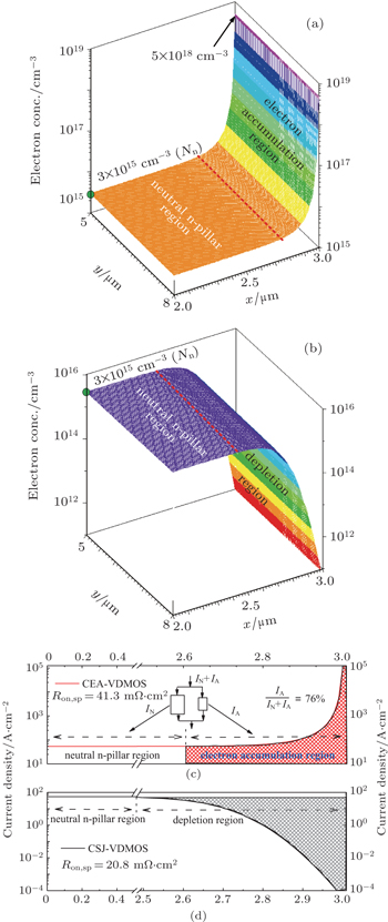
Figure 2 shows the on-state electron concentrations and current densities in the n-pillar of the CEA-VDMOS and CSJ-VDMOS (VGS = 15 V, VDS = 0.5 V). For the CEA-VDMOS, the electron concentration accumulated at the n-pillar sidewalls is up to 5 × 1018 cm−3, far higher than the doping concentration Nn of 3 × 1015 cm−3 as shown in Fig. 2(a). Therefore, approximately 76% of the current flows through the accumulation region and the maximum current density reaches up to 105 A·cm−2, which is three orders of magnitude higher than that of the neutral n-pillar region as shown with the red solid line in Fig. 2(c). However, for the CSJ-VDMOS, the electron concentration along the p-pillar/n-pillar interface is far lower than Nn due to the lateral depletion effect as shown in Fig. 2(b). Therefore, the current density (as shown in Fig. 2(d)) decreases, thus limiting the decrease in the Ron,sp of the CSJ-VDMOS. As a result, the CEA-VDMOS obtains an Ron,sp of 4.13 mΩ·cm2, much lower than the Ron,sp of 20.8 mΩ·cm2 for the CSJ-VDMOS.
The total on-state resistance of the CEA-VDMOS is composed of the accumulation layer resistance RA and neutral n-pillar region resistance RN in parallel. The RA (Ω) is given as

The RN (Ω) is shown as follows:

Then the total on-state resistance
R is given as

where
q is the magnitude of electronic charge;
μA and
μN are the electron mobility in the accumulation layer and neutral n-pillar drift, respectively;
ɛ0 is the permittivity of the free space;
ɛox is the relative permittivity of the oxide layer; and
VGS is the gate voltage.
For the CEA-VDMOS, owing to the fact that the RN and RA are in parallel (from Eq. (3)) and RA is smaller than RN, R is mainly determined by RA. Furthermore, the RA is independent of Nn according to Eq. (1). Then the variation of the Nn just influences the RN (Eq. (2)) and causes a little variation of Ron,sp. However, for the CSJ-VDMOS, the Ron,sp is almost determined by Nn and sensitive to the variation of Nn.
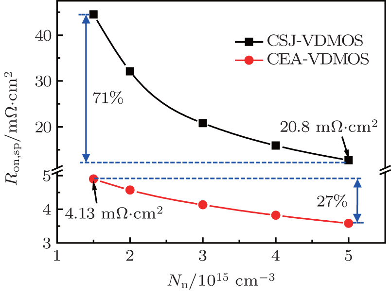
Figure 3 shows the plots of Ron,sp against Nn. As Nn decreases from 5 × 1015 cm−3 to 1.5 × 1015 cm−3, Ron,sp increases only 27% for the CEA-VDMOS, while it increases by 71% for the CSJ-VDMOS. It indicates that the Ron,sp of the CSJ-VDMOS depends on Nn, while the CEA-VDMOS relieves the Ron,sp from the strong restriction of Nn.
The IA and IN are the accumulation layer current and neutral n-pillar current, respectively, and η is defined as

where
IA is mostly determined by the
Tfox and
VGS according to Eq. (1), and
IN is mostly determined by the
W and
Nn according to Eq. (
2).
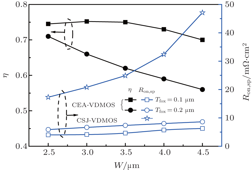
Figure 4 shows the influences of W and Tfox on η and Ron,sp. For the CSJ-VDMOS, the increase of W reduces the optimized Nn and increases the cell pitch, resulting in the sharp increase of Ron,sp. For the CEA-VDMOS, the increase of W causes IN to increase and η to decrease according to Eq. (1). Furthermore, owing to the most current flowing through the electron accumulation layers, i.e., IA≫ IN, the Ron,sp does not strongly depend on Nn and then increases slightly with the increase of W. Additionally, for the CEA-VDMOS, a larger IA is obtained for a thinner Tfox (Tfox = 0.1 μm) due to the enhanced accumulation effect and lowered RA according to Eq. (1), which leads to a larger η (Eq. (1)) and smaller Ron,sp.
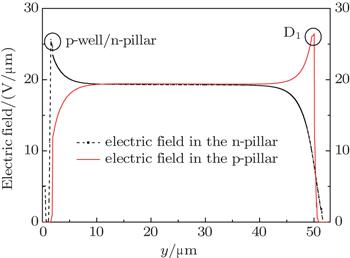
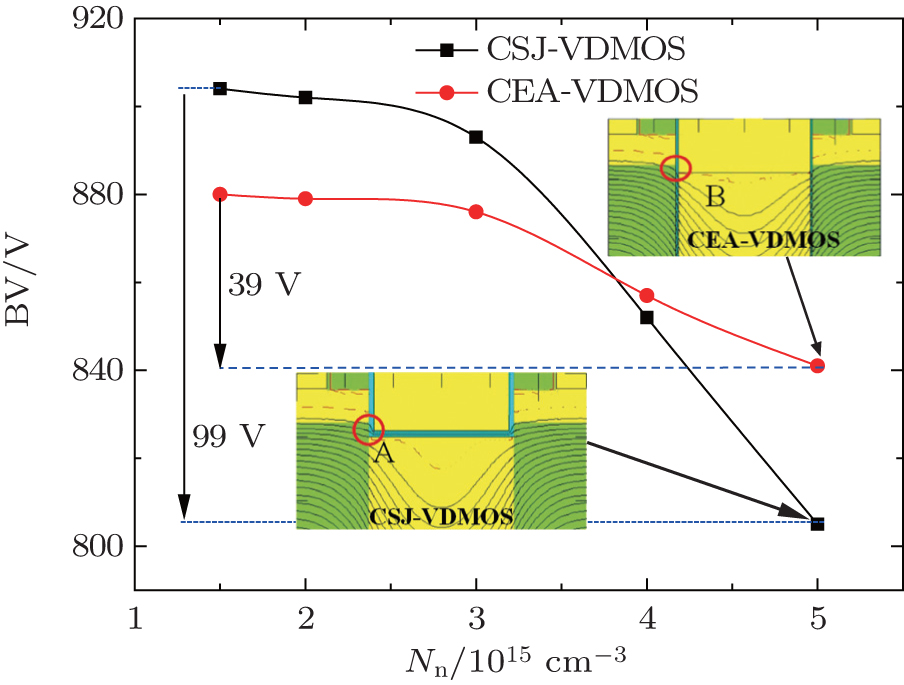
Figure 5 shows the electric field distributions in the n-pillar (black short dashed line) and p-pillar (red line) for the CEA-VDMOS in the off-state. The electric field peak in the n-pillar is located at the p-well/n-pillar junction, and the electric field peak in the p-pillar is located at D1 junction. Almost the same average electric field and electric field peak ensure the maximum breakdown voltage for the CEA-VDMOS.
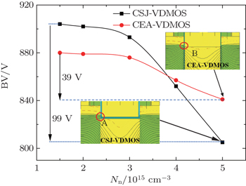
Figure 6 shows the plots of BV versus Nn for the CSJ-VDMOS and CEA-VDMOS. The simulation shows that the BV of the CEA-VDMOS is less sensitive to the variation of Nn than that of the CSJ-VDMOS. The Nn increases from 1.5 × 1015 cm−3 to 5 × 1015 cm−3, the BV of the CEA-VDMOS decreases by only 39 V, while that of the CSJ-VDMOS decreases by 99 V. The equipotential contours at breakdown for both devices are shown by the figures in the insets. For the CSJ-VDMOS, the equipotential contours are narrowed at the bottom of the trench gate (circle A), where a high peak electric field is caused and the premature breakdown is prone to occur with the increase of Nn. However, for the CEA-VDMOS, the equipotential contours are uniform at circle B. By the way, the maximum BV of the CEA-VDMOS is a little lower than that of the CSJ-VDMOS, owing to the fact that the N+ region in the trench stops the electric field prematurely, thus reducing the equivalent length of the voltage-sustaining region in the off-state for the CEA-VDMOS.
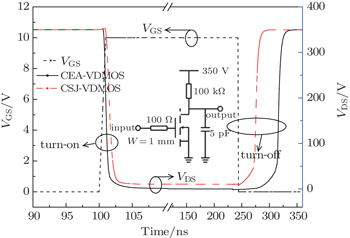
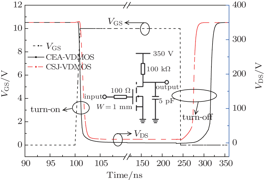
Figure 7 shows the comparison of switching characteristic between the CEA-VDMOS and the CSJ-VDMOS. From this figure, we can obtain that the ton = 0.8 ns and toff = 93 ns for the CEA-VDMOS as compared with ton = 1.2 ns and toff = 50 ns for the CSJ-VDMOS. The larger turn-off time for the CEA-VDMOS than that of the CSJ-VDMOS is mainly caused by a larger gate capacitance for the CEA-VDMOS. Considering the ultra-low Ron,sp and statics power dissipation, the CEA-VDMOS is more suitable for low and medium frequencies in the power field.
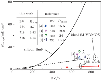
Figure 8 demonstrates the relationships between the Ron,sp and BV for the CEA-VDMOS and several power VDMOSFETs in the literature. The CEA-VDMOS obtains a much better trade-off between the BV and Ron,sp than other VDMOS mentioned above, breaks through the silicon limit of the conventional VDMOS, and shows significant superiority to the SJ VDMOS.
Figure 9 shows the feasible key process steps to fabricate a prototype of CEA-VDMOS: etch n-type epitaxial layer to form the deep trench with a depth of 50 μm and width of 6 μm, followed by peroxidation, oxide etch (to remove the etch damage) and then thermal oxidation to form a thin oxide layer with the thickness in a range of 0.1 μm–0.2 μm (see Fig. 9(a)); selectively etch the bottom oxide (see Fig. 9(b));[13–15] fill the trench with a certain doped p-type silicon, followed by implantation to form the N+ region (see Fig. 9(c)); choose low diffusion coefficient arsenic for accurate doping concentration and depth of the N+ region (see Fig. 9(d)); fill the trench with P-type doped silicon (see Fig. 9(e));[12] implant to form P-wells, gate contact P+ region and sources contact regions, then form the source/gate electrodes, followed by back-etching and forming the drain electrode (see Fig. 9(f)).


 , Wei Jie1, Tan Qiao1, Zhou Kun1, Wu Jun-Feng1]