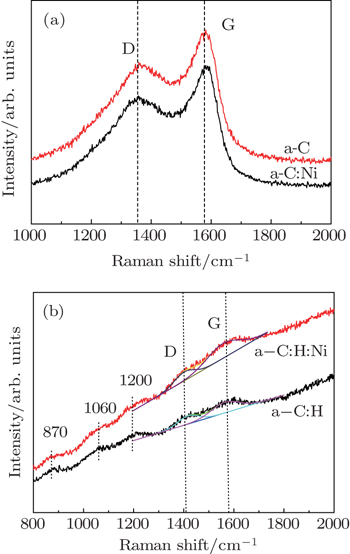
Field emission properties of a-C and a-C:H films deposited on silicon surfaces modified with nickel nanoparticles
Jiang Jin-Long1, †, , Wang Yu-Bao1, Wang Qiong1, Huang Hao1, Wei Zhi-Qiang1, Hao Jun-Ying2
Department of Physics, Lanzhou University of Technology, Lanzhou 730050, China
State Key Laboratory of Solid Lubrication, Lanzhou Institute of Chemical Physics, Chinese Academy of Sciences, Lanzhou 730000, China


† Corresponding author. E-mail: golden dragon@126.com

Project supported by the National Natural Science Foundation of China (Grant No. 51105186).

Abstract
Abstract

The a-C and a-C:H films are deposited on silicon surfaces modified with and without nickel nanoparticles by using mid-frequency magnetron sputtering. The microstructures and morphologies of the films are analyzed by Raman spectroscopy and atomic force microscopy. Field emission behaviors of the deposited films with and without nickel nanoparticles modification are comparatively investigated. It is found that the hydrogen-free carbon film exhibits a high field emission current density and low turn-on electric field compared with the hydrogenated carbon film. Nickel modifying could increase the current density, whereas it has no significant effect on the turn-on electric field. The mechanism of field electron emission of a sample is discussed from the surface morphologies of the films and nickel nanoparticle roles in the interface between film and substrate.

1. Introduction

Diamond-like carbon (DLC) films, including hydrogen-free amorphous carbon (a-C) and hydrogenated amorphous carbon (a-C:H) films, have attracted considerable attention to develop the advanced cold electron field emission materials for flat panel display and the vacuum microelectronic devices,[1] due to their negative electron affinities, low surface work functions, high thermal conductivities and outstanding chemical and physical stabilities.[2,3] However, so far the use of DLC film as a cold cathode has been restricted because of its low field emission current density. According to previous reports,[4,5] the field emission performance of DLC film was closely related to the surface morphology, composition (i.e., hydrogen content) and microstructure (i.e., sp2/sp3 bonding ratio). In recent years, great efforts have been devoted to the enhancement of the field emission properties of DLC films. Introducing the heteroatom dopant or nanoparticles into DLC film is an effective method to lower the threshold field value, increase the field current density, and enhance the field emission stability and durability.[610] Especially, transition metals, such as Ni and Fe were known to be very active to break and reform C–C bonds in a carbon matrix, which can strongly influence the microstructure of DLC film, thus further leading to the improvement of the field emission performance.[11,12] In these cases, the enhancement of the field emission is mainly attributed to the raised Fermi level, reduced work function, and enhanced conductivity.

The experimental and theoretical investigations have confirmed that the surface morphology is an important factor affecting the field emission properties of DLC film. The rough surface means more dense protrusions on the film surface, which could increase the field enhancement factor geometrically, thereby improving the field emission properties. Some efficient strategies have been used to produce protrusive surface structures. For example, Wei et al.[13] reported that the film surface turns from smooth to rough, becoming a peak-and-valley structure by the ion etching and bombarding method. Hart et al.[14] believed that plasma treatment can create sp2 clusters on the surface because it increased the field emission site density of the surface of DLC film.

As is well known, the surface roughness aspect of DLC film can also be controlled by the substrate roughness and can be maximized.[15,16] Therefore, in this work we prepare the a-C and a-C:H films by nickel nanoparticles modifying silicon substrate to regulate surface morphology using mid-frequency magnetron sputtering. The influence of nickel nanoparticle modification on the field emission property of the DLC film is comparatively investigated. To the best of our knowledge, there is no report on the field emission of DLC film deposited on Ni nanoparticles modified silicon substrate. The structures and surface morphologies of the films are investigated to clarify their field emission performances.

2. Experimental details
2.1. Film preparation

The n-Si (100) substrates were ultrasonically cleaned in alcohol and acetone. Ni nanoparticles (about 30 nm–80 nm in size) were ultrasonically dispersed in alcohol, and then dropped on the Si substrate surface. The silicon substrate modified with Ni nanoparticles was dried overnight in the atmospheric environment. Subsequently, the a-C films of approximately 180 nm in thickness were deposited on the pre-treated substrates by using mid-frequency magnetron sputtering graphite targets under 120-sccm Ar flow rate. The a-C:H films of approximately 1.2 μm in thickness were deposited by using mid-frequency magnetron sputtering graphite targets under a mixture atmosphere of 120-sccm Ar and 6-sccm CH4 flow rate. The background pressure was 3.9×10⁻³ Pa. The middle frequency (20 kHz) magnetron sputtering targets were operated at a constant current of 2.2 A with discharge voltages in ranges of 670 V–760 V for a-C films and 390 V–480 V for a-C:H films respectively. The plus bias voltage applied to the substrate was −50 V with 4-kHz frequency and 80% duty cycle. The deposition time was 90 min for all the films.

2.2. Film characterization

The surface morphologies and root-mean-square (RMS) surface roughness values of the films were acquired in tapping mode using an SPM (Nano IIIa) atomic force microscope (AFM). Raman spectra were recorded by a Horiba Jobin Yvon HR800 Raman spectrometer, with a 532-nm Ar ion laser used as an excitation resource. Field emission experiments were performed in a vacuum chamber with a pressure of 1.0×10⁻⁶ Pa. The measurements were conducted on a standard parallel-plate-electrode configuration where a stainless-steel plate was used as an anode current collector, and the film fixed onto a copper stage with conductive tape served as a cathode.[17] The distance between the film surface and the anode was adjusted to about 300 μm by a spiral micrometer prior to the measurements. The voltage was applied from 300 V to 3600 V in steps of 30 V. The anode and the cathode were connected by a computer-controlled Keithley 248 source meter to record the corresponding current.

3. Results and discussion
3.1. Raman spectra

Figure 1(a) shows the Raman spectra of a-C and a-C:Ni films. It can be seen that the visible Raman spectra of a-C films were located at approximately 1370 cm−1 and 1580 cm−1, which were referred to as the D peak and G peak, respectively.[18] This suggests that the films are typical DLC films with mixed structures of sp2 and sp3 carbon. The peak at 1370 cm−1 drives from the A1g breathing mode of the sp2 ring structure in disorder graphite, while the peak at 1580 cm−1 can be identified with the E2g vibrational mode arising from the bond stretching of all pairs of sp2 atoms in both rings and chains. There is no variation in the peak position nor shape nor intensity of the Raman spectrum after Ni nanoparticles have modified the substrate surface. This indicates that neither the sp3 carbon content nor sp2 clustering is significantly changed in each of the films.

Fig. 1. Raman spectra of the as-deposited films: (a) a-C, a-C:Ni and (b) a-C:H, a-C:H:Ni.

Figure 1(b) shows the Raman spectra of a-C:H and a-C:H:Ni films. It is observed that the peaks in Raman spectra of a-C:H and a-C:H:Ni films are overshadowed by the strongly photoluminescence background, which is attributed to the hydrogen saturation of nonradiative recombination centers due to the high hydrogen content in each of the films.[19] Even so, there are still five peaks that appear which are clearly distinguishable in a range of 800 cm−1–2000 cm−1 of Raman spectra, which are also observed and referred in Ref. [20]. Casiraghi et al.[21] reported that the bonding hydrogen content can be estimated by an empirical equation. A typical signature of the visible Raman spectrum for a-C:H film is the increasing photoluminescence background when increasing hydrogen content. Thus, it could be concluded that the a-C:H:Ni film possesses a higher bonding hydrogen content. Raman spectra in a range of 1200 cm−1–1800 cm−1 are further fitted to two Gaussian peaks in order to distinguish the structure changes of the film. It is found that the G peak position shifts from 1562 cm−1 to a lower wavenumber of 1557 cm−1, which suggests the increasing of sp3 carbon content in the a-C:H:Ni film.
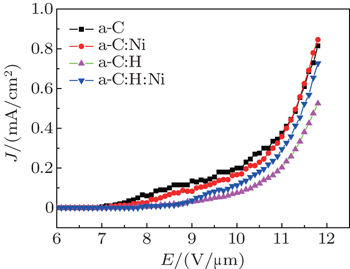
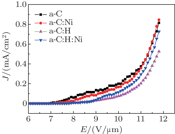
3.2. Surface morphology

Figure 2 shows the AFM images of the deposited films. It can be observed that the a-C film displays a smoother and more uniform surface. The micro-protrusion on the surface of the a-C:Ni film is more and larger than on the surface of the a-C film. The root mean square (RMS) surface roughness values of the films within the surface area of 3 μm×3 μm are demonstrated in Fig. 3. Compared with the a-C film, the a-C:Ni film exhibits a considerably rough surface with a 27-nm RMS roughness value. The a-C:H and a-C:H:Ni films exhibit the smoother surfaces, each of which is composed of uniform and compact particles. The RMS roughness of a-C:H:Ni film is about 5.5 nm, which is only slightly higher than that of a-C:H film (3.9 nm). It is notable that Ni nanoparticles modified substrate surface leads to a marked increase in surface roughness of the a-C film, but only a little change in the a-C:H film. During the growth of the film, the incident energetic ions in the plasma can bombard and etch the growing surface, which causes the smoother surface. In the growth process of a-C:H:Ni film, apart from Ar ions, the methane gas as a carbon source are decomposed into some hydrocarbon neutral radicals, ionic radicals and atomic or ionic hydrogen in magnetron charging, leading to an increase of the bombardment and etching effect. Therefore, RMS surface roughness of the hydrogenated films is lower than that of the hydrogen-free film. Consequently, the difference in RMS surface roughness value between the a-C and a-C:N films is more obvious than between the a-C:H and a-C:H:Ni films.

Fig. 2. AFM images of the deposited films: (a) a-C, (b) a-C:Ni, (c) a-C:H, (d) a-C:H:Ni.
Fig. 3. RMS surface roughness values of the deposited films.
3.3. Field emission properties

Figure 4 shows the variations of field emission current density (J) of the films with applied electric field (E). The field emission current density is determined from the formula, J = I/S, where I is the field emission current and S is the entire area of the sample exposed to the anode screen. The electric field E is determined from the formula, E = V/d, where V is the applied voltage and d is an anode-to-cathode distance. For the a-C film, the turn-on electric field, which is defined as the electric field extracted at an emission current density of 10 μA/cm2, is 7.1 V/μm, and the maximum current density is 815 μA/cm2 at an applied electric field of 11.8 V/μm. Compared with the a-C film, the a-C:Ni film possesses a turn-on electric field of 7.4 V/μm and a maximum current density of 846 μA/cm2 at 11.8 V/μm. On the other hand, it can be observed that the turn-on electric fields are 8.3 V/μm and 8.4 V/μm for a-C:H film and a-C:H:Ni film, respectively. Although Ni nanoparticle modification does not reduce the turn-on field of the a-C:H film, it markedly enhances the current density from 525 μA/cm2 to 727 μA/cm2 at an electric field of 11.8 V/μm. Furthermore, the hydrogen-free DLC films show better field emission performances than the hydrogenated DLC films, no matter whether Ni nanoparticles modify the substrate surface or not. This result could mainly be attributed to the low defect state in the form of spin density and high band gap in the a-C:H film due to high C-H sp3 bond hybridization.[22] Park et al.[23] found that the field emission current increases and turn-on field decreases with the decrease of hydrogen content in the DLC film.

Fig. 4. Variations of field emission current density of the film with applied electric field.

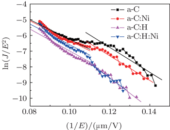
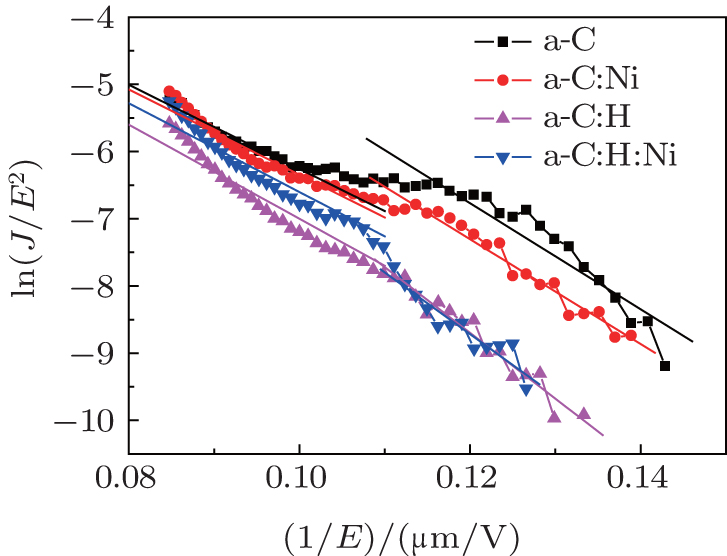
The Fowler–Nordheim (FN) plots of the films, i.e., plots of ln (J/E2) versus 1/E, are obtained in Fig. 5. According to the FN theory, the electron field emission behavior obeys the following FN equation[24] containing the work function under the external applied field:

where J is the field emission current density in units A/m2, E is the applied electric field in units V/μm, Φ is the work function in unit eV, β is the field enhancement factor at sharp geometries, and A and B are constants (A = 1.56×10⁻², and B = 6.8×10⁹). If the electron emission is controlled by the tunneling effect, the FN plot presents a nearly straight line with a negative slope which is the normal test for the field emission process.[25] Here, the FN plots could not be fitted to the good straight lines in the whole electric field range, implying the different electron emission mechanisms. This nonlinear behavior of the FN plot was observed by Yang et al.,[26] and Zhang et al.,[27] which was proposed as a consequence of the emission of thermal electrons at high temperature caused by the high current. However, it can be seen that FN plots are nearly linear in a low electric field and high electric field, respectively, which is in good agreement with FN theory. Li et al. believed that this would correspond to field emission from two different kinds of emission sites: one is the sp3 site with a low effective work function, which could provide the low-field part of the emission, and the other is the sp2 cluster with a higher effective work function, which begins to emit electrons as the applied voltage rises up.[10] Assuming that the field enhancement factor β is 1, the slope of the FN curve would be −
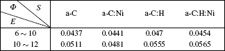
 3/2. The corresponding work functions of the samples are calculated according to the slopes of the plots in Fig. 5. The results are shown in Table 1. Actually, the real values of the work function for carbon films are 3.5 eV–4.0 eV, which are larger than the calculations. Such low work functions are due to the underestimation of the field enhancement factor.

Fig. 5. Fowler-Nordheim plots of the films.
Table 1.

Work functions of the films at low and high electric field parts. The parameters Φ in unit eV and E in units V·μm−1.

.

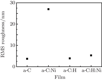
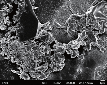
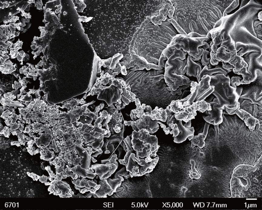
Moreover, besides surface roughening, the role of nickel nanoparticles in transport of electrons is also important, which should be considered in this case. On the one hand, it is reasonable to believe that the nickel modification can offer the higher conductivity between the film and silicon substrate, which is beneficial to transport of field electrons. However, on the other hand, the nickel modification reduces the adhesion between film and silicon substrate, leading to the wrinkles, cracks and even partly peeling off from the substrate as shown in Fig. 6, owing to the high internal stresses in the hydrogen-free films. The failure of the interface would give a special barrier for the transport of field emission electrons. Hence, although Ni nanoparticle modification leads to the remarkable increase in surface roughness, the emission current for a-C:Ni film is only slightly enhanced.

Fig. 6. SEM image of a-C:Ni film after stress relaxation.
4. Conclusions

In this paper, we report the field-emission properties of the a-C and a-C:H films deposited on silicon surfaces modified with and without nickel nanoparticles by mid-frequency magnetron sputtering. It is shown that the hydrogen-free DLC film exhibits the higher field emission current density and lower turn-on electric field than the hydrogenated DLC film. The Ni nanoparticle modification can improve the field-emission performance of the DLC film. Especially, the field emission current density slightly increases from 815 μA/cm2 to 846 μA/cm2 for the hydrogen-free DLC film, whereas it markedly increases from 525 μA/cm2 to 727 μA/cm2 for the hydrogenated DLC film. There are no distinct changes in the turn-on electric field of the film before and after modification.

Reference
1Xu JXu PWei O YChen XGuo PLi JPiao XWang MSun Z 2015 Appl. Phys. Lett. 106 073501
2Robertson J 1997 Thin Solid Films 296 61
3Ahmed S FMoon M WLee K R 2008 Appl. Phys. Lett. 92 193502
4Xu JHuang X HLi Z FLi WChen K J 2003 Diamond Relat. Mater. 12 2016
5Xie W GChen JChen JDeng S ZShe J CXu N S 2007 J. Appl. Phys. 101 084315
6Zanin HMay P WHamanaka M H M OCorat E J 2013 ACS Appl. Mater. Interfaces 5 12238
7Dwivedi NKumar SCarey J DTripathi R KMalik H KDalai M K 2013 ACS Appl. Mater. Interfaces 5 2725
8Wan S HWang L PZhang J YXue Q J 2009 Appl. Surf. Sci. 255 3817
9Zhang PLi R SYang HFeng Y CXie E Q 2012 Solid State Sci. 14 715
10Li R SXie E QZhou MZhang Z XWang TLu B A 2008 Appl. Surf. Sci. 255 2787
11Ling X MZhang P ZLi R SFan D WYao X M 2013 Surf. Interface Anal. 45 943
12Wang QLi S LWan S H 2012 Physica E: Low Dimensional Systems and Nanostructures 46 89
13Wei S BShao T MXu J 2012 Surf. Coat. Technol. 206 3944
14Hart ASatyanarayana B SMilne W IRobertson J 1999 Appl. Phys. Lett. 74 1594
15Erdemir ADonnet C 2006 J. Phys. D: Appl. Phys. 39 311
16Zhong MZhang C HLuo J B 2008 Appl. Surf. Sci. 254 6742
17Li JChen J TLuo B MYan X BXue Q J 2012 AIP Adv. 2 022101
18Ferrari A CRobertson J 2000 Phys. Rev. 61 14095
19Jiang J LWang QHuang HZhang XWang Y BGeng Q F 2014 J. Inorg. Mater. 29 941
20Jiang J LHao J YWang PLiu W M 2010 J. Appl. Phys. 108 033510
21Casiraghi CFerrari A CRobertson J 2005 Phys. Rev. 72 085401
22Siliva S R PCarey J DGuo XTsang W MPoa C H P 2005 Thin Solid Films 482 79
23Park K CMoon J HChung S JOh M HMilne W IJang J19969th International Vacuum Microelectronics Conference (IVMC–96) 1996 St. Petersburg 268
24Satyanarayana B SHart AMilne W IRobertson J 1997 Appl. Phys. Lett. 71 1430
25Fowler R HNordheim L 1928 Proc. R. Soc. 119 173
26Yang JYan XChen JSun DXue Q 2014 Chin. Chem. Lett. 25 375
27Zhang X HGong LLiu KCao YXiao XSun WHu XGao YChen JZhou JWang Z L 2010 Adv. Mater. 22 5292