Modulating doping and interface magnetism of epitaxial graphene on SiC(0001)
Zhou Pan , He Da-Wei †,
Key Laboratory of Luminescence and Optical Information, Ministry of Education, Institute of Optoelectronic Technology, Beijing Jiaotong University, Beijing 100044, China


† Corresponding author. E-mail: dwhe@bjtu.edu.cn

Project supported by the National Natural Science Foundation of China (Grant Nos. 61335006, 61378073, and 61527817), the Beijing Municipal Science and Technology Committee, China (Grant No. Z151100003315006), and Fundamental Research Funds for the Central Universities of Beijing Jiaotong University, China (Grant No. 2012YJS123).

Abstract
Abstract

On the basis of first principles calculations, we report that the type and density of charge carriers of epitaxial graphene on SiC(0001) can be deliberately controlled by decorating the buffer layer with specific atoms (i.e., F, Cl, O, or N). More importantly, a fine tuning of the doping behavior from intrinsic n-type to charge neutrality to p-type and interface magnetism is achieved via increasing the doping concentration of F atoms on the buffer layer. Our results suggest an interesting avenue to the application of epitaxial graphene in nanoscale electronic and spintronic devices.

1. Introduction

The distinct electronic structure and physical properties of graphene [ 1 4 ] or graphene-like two-dimensional materials [ 5 ] have aroused considerable interest. More particularly, graphene has been made a candidate of Si in the post-Moore era. [ 6 9 ] Nevertheless, the successful development of graphene-based electronics requires the large-scale synthesis of high-quality graphene. The epitaxial growth of graphene on SiC(0001) or via high temperature annealing is a promising fabrication strategy for technological application. [ 10 13 ] Most importantly, the fine controlling of the number of graphene layers has been realized [ 14 , 15 ] on SiC(0001). The first graphene layer, acting as a buffer layer, is covalently bonded to the Si-terminated substrate fitting into a reconstruction, [ 13 , 16 18 ] resulting in distortion in the linear dispersion near E D . This characteristic spectrum of freestanding graphene is recovered with the second carbon layer. [ 19 , 20 ] However, the first few layers in epitaxial graphene are electron doped by charge transfer from the substrate. [ 21 24 ] As is well known, the precise control of the type and concentration of charge carriers is at the heart of modern electronics. Therefore, counteracting this intrinsic electron doping to achieve charge neutrality or hole doping is also desirable for practical application of epitaxial graphene to electronic devices. Recent experiment and theory have shown that the epitaxial graphene on SiC exhibits a transition from n-type to p-type under a top-gated voltage. [ 25 , 26 ] Surface doping by external chemical species, such as NO 2 molecules, [ 27 ] tetrafluorotetracyanoquinodimethane (F4-TCNQ) molecules, [ 28 , 29 ] hydrogen atomics, [ 10 ] or atomic layers of bismuth, antimony and gold, [ 30 ] is also an effective way to tune the carriers’ properties.

On the other hand, interface engineering has been widely used to modify the structural and electronic properties in the heterojunctions, such as BNC system, [ 31 ] carbon nanotubes on InAs(111), [ 32 ] Si(0001) [ 33 ] surface, epitaxial graphene on Ir(111). [ 34 ] Wang et al. proposed that n-doped or p-doped graphene sheets on a chip could be achieved by modifying the SiO 2 substrate with self-assembled layers of silane and polymer in experiment. [ 35 ] Indeed, in the system of epitaxial graphene on SiC, Zhou et al. experimentally showed that the doping of graphene was associated with the surface charges at the interface, rather than the carrier concentration of the substrate. [ 36 ] Thus the first graphene layer and surface of the substrate, acting as the interface, offer the possibility of using them for band engineering of the system. [ 37 , 38 ] Some studies introduced a configuration with graphene/intercalated atoms/substrate for investigating the decoupling of graphene and substrates by other atoms. [ 10 , 34 , 39 ] In the system of epitaxial graphene on Si-terminated substrate, the first graphene layer and the substrate are linked by covalent bonds, which need high energy consumption to be broken up. Meanwhile, the first and second graphene layers are held together by van der Waals force. The interlamination between the two graphene layers is relatively large. Therefore, it is easier for atoms to be intercalated between the graphene layers. Therefore, we mainly focus on the second case in this paper.

In this paper, employing ab initio density functional theoretical calculations, we show both the type of epitaxial graphene and the density of epitaxial graphene atoms on SiC(0001) can be deliberately controlled via decorating the buffer layer with specific atoms (i.e., F, Cl, O, N). More importantly, the fine tuning of the doping behavior from intrinsic n-type to charge neutrality to p-type and interface magnetism are achieved by increasing the adsorption concentration of F atoms on the buffer layer. For other atom doping cases, Cl doping has similar effects to the F doping, and N decoration is an effective way to induce a metal-semiconductor transition with the Dirac point moving but not disappearing, while O modification leads to a p-type doping. There have been experimental research studies of intercalation of F atoms [ 10 ] and the intercalation of O atoms, [ 40 ] but not on the intercalation of N atoms. As mentioned above, it is easier for atoms to be intercalated between the graphene layers. After intercalation, F atoms and O atoms may be adsorbed on the surface of the first graphene layer, while N atoms are more likely to link the first and second graphene layers. These are the atomic structures to be studied in this paper.

2. Computational methods

Our calculations are performed in the framework of density functional theory (DFT) as implemented in the PWSCF code. [ 41 ] The local spin density (LDA) approximation and projector augmented wave (PAW) potentials are used to describe electronic exchange–correlation and electron–core interactions, respectively. A kinetic cutoff of 400 eV is used in the plane wave expansion. The systems studied here consist of one, two or three carbon layers with Bernal stacking on 6H-SiC(0001) substrate. We adopt a
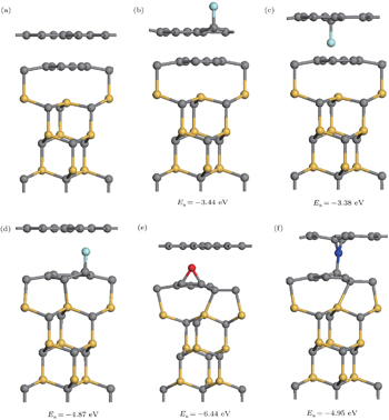
 substrate cell to accommodate a 2 × 2 graphene cell, as an approximation of the realistic model, which is too complicated to be computed. The substrate is simulated by six SiC bilayers with H saturated dangling bonds on the bottom surface. The vacuum space of at least of 12 Å is chosen to eliminate the interaction between the slabs. The Monkhorst–Pack k -points samplings of 7 × 7 × 1 and 15 × 15 × 1 grids are used for geometric relaxations and electronic structure calculations, respectively. All structures are fully optimized until the Helmann–Feynman force on each atom is less than 0.02 eV/Å.

3. Results and discussion

As shown in Fig. 1(a) , for the pristine system, there are three Si atoms at the surface of SiC substrate in a unit cell. Two of them are covalently bonded with the C atoms in the first graphene layer, with a bond length of 2.0 Å, while the third exhibits a dangling bond pointing toward the center of the top C hexagonal lattice, with a distance of 2.55 Å, consistent with the previous report. [ 20 ] Thus the first C layer is found to be corrugated and behaves as a buffer layer, while the subsequent layers display perfect planar honeycomb structures. The interlayer distance between the second graphene layer and the rippled buffer layer is between 3.24 and 3.52 Å. Following the current convention, for the C atoms in the buffer layer, we define the ones bonded to Si as C b and the others which are not bonded to Si as C l . Since the corrugation can enhance the chemical activity of graphene to some extent, [ 42 ] the doping of the buffer layer is expected to be easier than that of the other C layer. However, to manipulate carriers, another important question is to search for suitable p/n-type dopants. Adsorbates which are much more electronegative than C can act as electron acceptors, thus providing an effective way to counteract intrinsic electron doping. Here, F doping is considered first. For two graphene layers on the Si terminated substrate, we check all the possible adsorption sites, with some typical ones shown in Figs. 1(b) 1(d) , and calculate the corresponding average adsorption energies to find the stablest configuration. The average adsorption energy ( E a ) is defined as E a = [ E SiC-GR-adatoms E SiC-GR E adatom n ]/ n , where E SiC-GR-adatoms , E SiC-GR , E adatom are the total energies of doped system, perfect system, and a single isolated adatom, respectively. As shown in Fig. 1(b) , when F is adsorbed on the top surface of the second graphene layer, the interlayer distance varies between 3.00 Å and 3.58 Å, with E a being −3.44 eV. However, when F is bonded to the bottom surface of the second graphene layer [see Fig. 1(c) ], the interlayer distance increases dramatically, varying between 3.77 Å and 4.29 Å, with E a being −3.38 eV. The variations of the two adsorption energies can be exactly explained by the difference in the interlayer distance between the two cases. Theoretically, for moving from the top surface to the bottom surface of the second graphene layer, the F atoms need to cross a hexatomic ring of graphene. The energy barrier is higher than 3 eV, which means that it is not feasible to change from the state in Fig. 1(b) to the state in Fig. 1(c) . But the state in Fig. 1(c) can be actualized in experiment, as F atoms may directly move into the interlamination and then are adsorbed at the bottom surface of the second graphene layer. At the buffer layer, F inclines to bond with C l , rather than the sp 3 hybridized C b [Fig. 1(c) ]. The corresponding C–F bond length is 1.41 Å, and the E a is −4.87 eV in this case, which is ∼ 1.4 eV larger than those of other adsorption cases. The fluorinated C l transforms from sp 2 to sp 3 hybridization, This implies that when the F atom is intercalated into the interlamination of epitaxial graphene, its change will be captured preferentially by the rippled buffer layer. The original DB is saturated by the nearest top C l atom, with the Si–C bond length being 2.14 Å, because the F adsorption increases the local deformation of the first C layer.

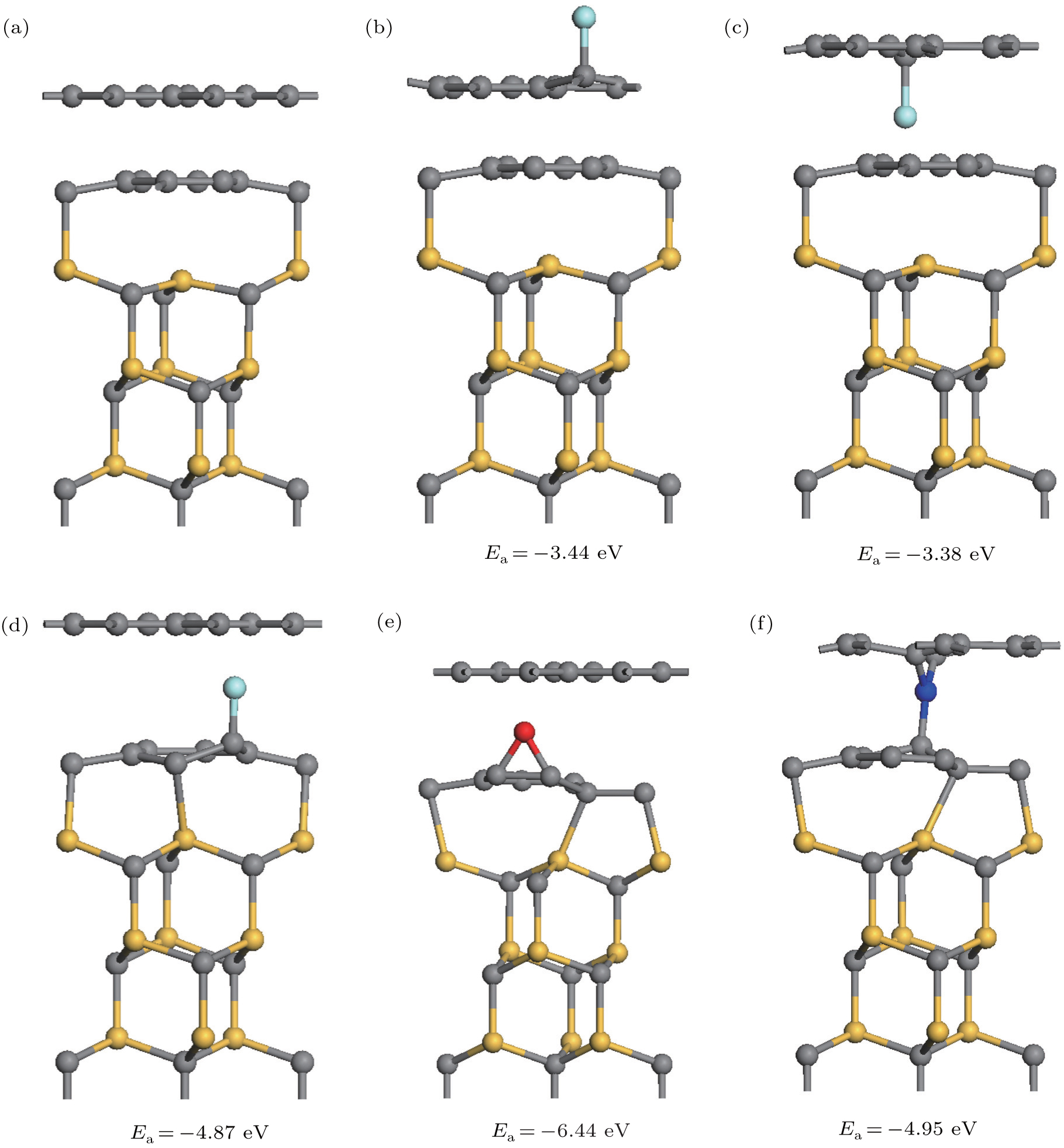
Fig. 1. Optimized structures of perfect and doped epitaxial graphene on SiC(0001). (a) perfect system. (b)–(d) F decorated systems with different adsorption sites. (d) and (e) The stablest configurations of O, N decorated epitaxial graphene.
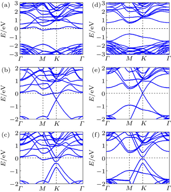
Figure 2 shows the electronic structures of one, two, or three graphene layers on SiC(0001) with the first layer decorated by a single F atom. In comparison, we plot electronic structures of corresponding perfect epitaxial graphene in Figs. 2(a) 2(c) . It can be easily seen that all three perfect epitaxial graphene layers are all n-type doped, which is consistent with previous studies. [ 19 , 20 ] For a single graphene layer on SiC(0001), its band structure significantly differs from that of the isolated graphene and exhibits a wide energy gap of 1.66 eV. The graphene related linear dispersion appears when the second layer is added on top of the first one and the Dirac point falls 0.45 eV below the Fermi level. When there are three C layers, the dispersion is similar to that of the isolated bilayer graphene, but the band shift induced by intrinsic electron doping is slightly (about 0.35 eV) lower than that of the epitaxial bilayer. In addition, the built-in dipole field at the SiC-graphene interface breaks the symmetry of the bilayer on the buffer layer, [ 21 , 22 , 36 ] rendering a band gap opened by 0.13 eV. This band gap is highly crucial for the application of epitaxial graphene in nanoelectronics, however, the gap lies below E F , which will restrict its application. Interestingly, when the first C layer is doped by an F atom, the Fermi level shifts downward into the band gap (for the monolayer and three layers) or to the Dirac point (for the bilayer). The weakly dispersive state at the E F which is related to the DB at the interface [ 19 ] of the perfect epitaxial graphene disappears because the original dangling bond is saturated after the single F adsorption. Most importantly, although the buffer layer is decorated by an F atom, additional states are not introduced near the Fermi level because F chemically bonds with the C atom and its orbits are located deeply below the Fermi level. Moreover the typical electronic structures like graphene [Fig. 2(b) ] and bilayer graphene [Fig. 2(c) ] are not destroyed, and the electronic properties are dominated by the C layers on the buffer layer.

Fig. 2. Band structures for one ((a) and (d)), two ((b) and (e)), three ((c) and (f)) carbon layers on the SiC(0001). Curves in panels (a)–(c) correspond to the perfect systems, while the curves in panels (d)–(f) correspond to the doped system with the first C layer decorated by one F atom.

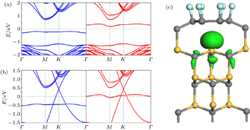
Next, we increase the adsorption concentration of F atoms until all the C l atoms in the buffer layer are adsorbed by F atoms, that is, six F adatoms in the unit cell. Unlike the case of single F decoration, one third of Si atoms at the interface are not saturated, like a perfect system. However, the DB related interface state of the six F atom doped system shows different behaviors from those of the perfect system. Figure 3(a) shows the band structures for one graphene layer with six-F-atom decoration on SiC(0001). We find that the interface state is split into an occupied state and an unoccupied state, whereas it is a half-filled metallic state in the perfect system [see Fig. 1(a) ]. The significant differences can be clearly understood if one compares the band decomposed charge densities of two kinds of interface states. For a perfect system, its interface state is not localized, which results from the hybridization of the dangling orbit of the Si atom with the quasi-delocalized π network of the buffer layer. In contrast, after the full fluorination of the C l atoms, strong σ -bonds form between C l and F atoms, completely breaking the extensive π -bonding network. Thus the unsaturated Si atom at the interface has little interaction with the buffer layer, resulting in a very localized interface state. Given the localized character of the interface state, the electron hopping integral is expected to be small, while the Hubbard repulsion of electrons would be large and split the half filled band into halves, which have about 0.3 eV above and below the E F , inducing spin polarization. The spin density distribution [Fig. 3(c) ] also shows that the induced magnetic moments are mostly localized on the dangling Si atom. With additional perfect graphene layer present on this F decorated buffer layer, the system is still spin polarized. Most interestingly, its linear dispersion is retained, but the Dirac points are 0.42 eV above the E F for both of the major and minority spins [see Fig. 3(b) ]. This shows that a strong p-type doping of epitaxial graphene is achieved. In addition, the DB state crosses with the typical linear π bands originating from the second quasi-free-standing graphene, implying that we can mediate the DB induced magnetism through its interaction with the itinerant π electrons.

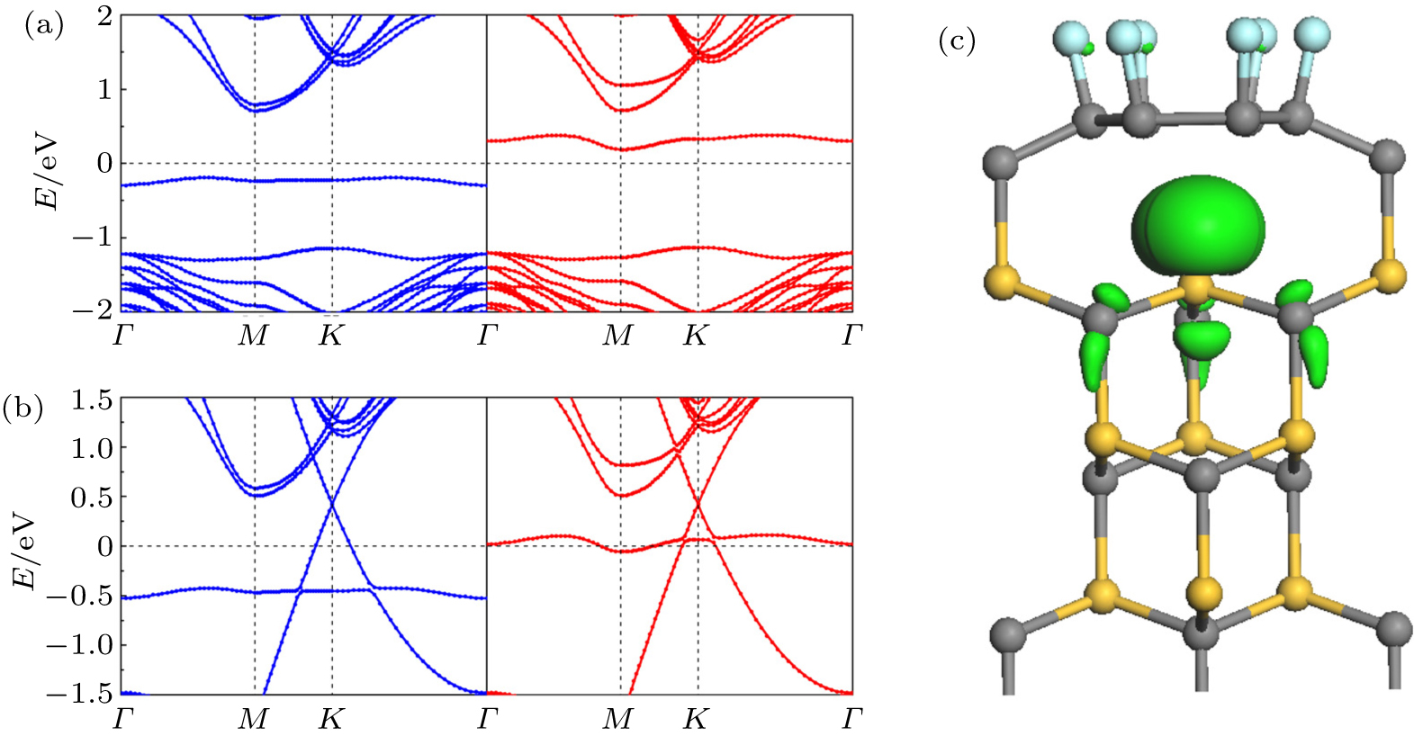
Fig. 3. Band structures for (a) one and (b) two graphene layers on SiC(0001) with the first graphene layer doped by six F atoms. The blue and red curves represent the majority and minority spin, respectively. (c) Spin density ( ρ = ρ ↑ − ρ ↓) isosurfaces of the six F atoms decorated single layer epitaxial graphene. The isosurface is 0.025 e/Å 3 .

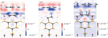
So far, by analyzing the band structures, we know that the doping behaviors of the epitaxial graphene can be finely tuned from intrinsic n-type to charge neutrality to p-type by increasing the doping concentration of F atoms on the buffer layer. Then we turn to investigate how the F dopants tune the carrier properties and charge transfer. Taking the systems containing two graphene layers on the SiC for example, figures 4(a) 4(c) show the contour plots of the charge density difference, defined as Δ ρ = ρ tot ρ toplayer ρ sub+buffer , where ρ tot , ρ toplayer , and ρ sub+buffer are the charge densities of the total system, the isolated top graphene, and the isolated substrate and buffer layer (pure or doped), respectively. The last two terms, ρ toplayer and ρ sub+buffer , are calculated by keeping the same equilibrium geometry as that of the total system. For the perfect system, as shown in Fig. 4(a) , the charge accumulation is localized on the top layer, while the charge depletion is concentrated near the buffer layer. With one F atom decorating the buffer layer, the charge accumulation and depletion are both assembled on the top C layer [see Fig. 4(b) ], so the top layer experiences a transition from n-type to neutrality. When more F atoms are adsorbed on the buffer layer, a pronounced charge is transferred to the F adsorbed buffer layer, and the charge depletion now takes place on the top layer [see Fig. 4(d) ], causing a p-type doping of the top graphene layer.

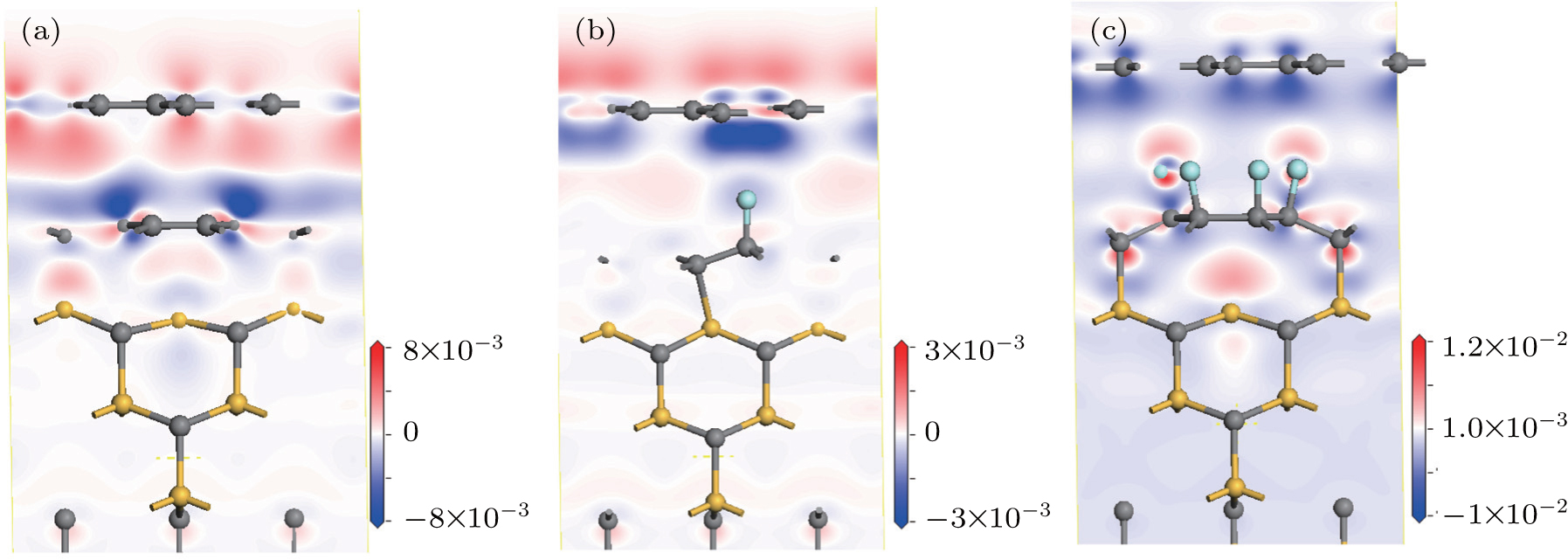
Fig. 4. Contour plots of charge density difference of perfect system (a), single F atom decorated system (b), and six F atoms decorated system (c). Gray, yellow, and blue balls denote C, N, and F atoms, respectively.

In addition, we also use Bader analysis, a measure of charge quantity localized around a given atomic site, to give a quantitative estimate of the charge variations of the F atoms and graphene layers. For the perfect system, the electron densities in the buffer layer and the top layer are ∼ 4.88 × 10 14 cm −2 and ∼ 3.85 × 10 13 cm −2 , respectively, consistent with its n-doped band structure. When the buffer layer is doped by an F atom, owing to the formation of another C–Si bond, an additional 0.44 electrons are transferred from the substrate. On the other hand, the F atom shows an onsite charge quantity of 7.64 e, which means that there are 0.64 holes injected into the graphene layer. This is due to the larger electronegativity of F than that of C. Thus, the electron density in the buffer layer is reduced to ∼ 4.50 × 10 14 cm −2 , showing a modest decrease. Most importantly, there is no charge transfer to the top graphene layer, which makes the Dirac point of the top layer lay exactly at the Fermi level. When the buffer is adsorbed by six F atoms, with each F atom accepting 0.59 e, enough holes are injected into the graphene layers, part of which can neutralize the electrons transferred from the substrate. Then the buffer layer and top layer transform into p-type, exhibiting hole densities of ∼ 8.59 × 10 14 cm −2 and ∼ 4.51 × 10 13 cm −2 , respectively.

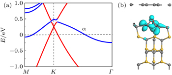
Finally, we investigate the effects of the doping of other atoms (i.e., Cl, O, and N) on the buffer layer. Since Cl and F subordinate to the same main group, similar configurations and behaviors as discussed above are found. However, O doping on buffer layer shows quite different behaviors. As shown in Fig. 1(e) , it prefers to bond with two C l atoms. The local deformation of buffer layer resulting from O adsorption induces the saturation of original DB of Si at the interface by the top C l atom, with a Si–C bond length of 2.06 Å. The C–O bond length is 1.43 Å and the adsorption energy is −6.44 eV. Figure 5(a) displays the corresponding band structure, where we can find that the Fermi level is about 0.25 eV below the Dirac point, showing a p-type doping behavior. The linear dispersion is modulated by the α band interacting with the unoccupied π * band, opening a tiny gap of 40 meV about the E F . Figure 5(b) shows the plot of the partial charge density of the α band at characteristic Γ point. One can see that the α band is almost entirely distributed by the O doped buffer layer.

Table 1.

Manipulations of carrier type and gap in graphene by atoms (F, Cl, O, N) intercalations. F, or Cl, or O intercalation leads to a p-type doping in graphene, but cannot open the band gap of graphene. N intercalation cannot bring in external carriers but renders a band gap opening, and the band gap is 0.25 eV.

.
Fig. 5. (a) Band structure of bilayer graphene with buffer layer doped by O on SiC(0001), with the top graphene energy bands being highlighted by red lines. (b) Partial charge density of the α band at the Γ point. The isosurface is 0.05 e/Å 3 . Gray, yellow, and red balls denote C, Si, and O atoms, respectively.

Figure 1(f) shows the structure of N intercalation in the epitaxial graphene. Since N has three unpaired p electrons in its outer electron shell, the system is stablest when it interacts with two C atoms in the top layer and one C atom in the buffer layer to form sp 3 nonequivalent hybridization, with an adsorption energy of −4.95 eV. The three C–N bonds lengths are 1.387 Å, 1.384 Å (bonding with top layer), and 1.452 Å (bonding with buffer layer), respectively. Because the top C layer forms strong σ bond with N atom, the location of the Dirac point moves, not at K point as shown in Fig. 6(a) . Besides, a gap of 70 meV is opened and Fermi level is shifted into the middle of the gap. The system experiences a metal-semiconductor transition. The LDOS (Fig. 6(b) ) clearly shows the states near the Fermi level are totally contributed by the top C layer.

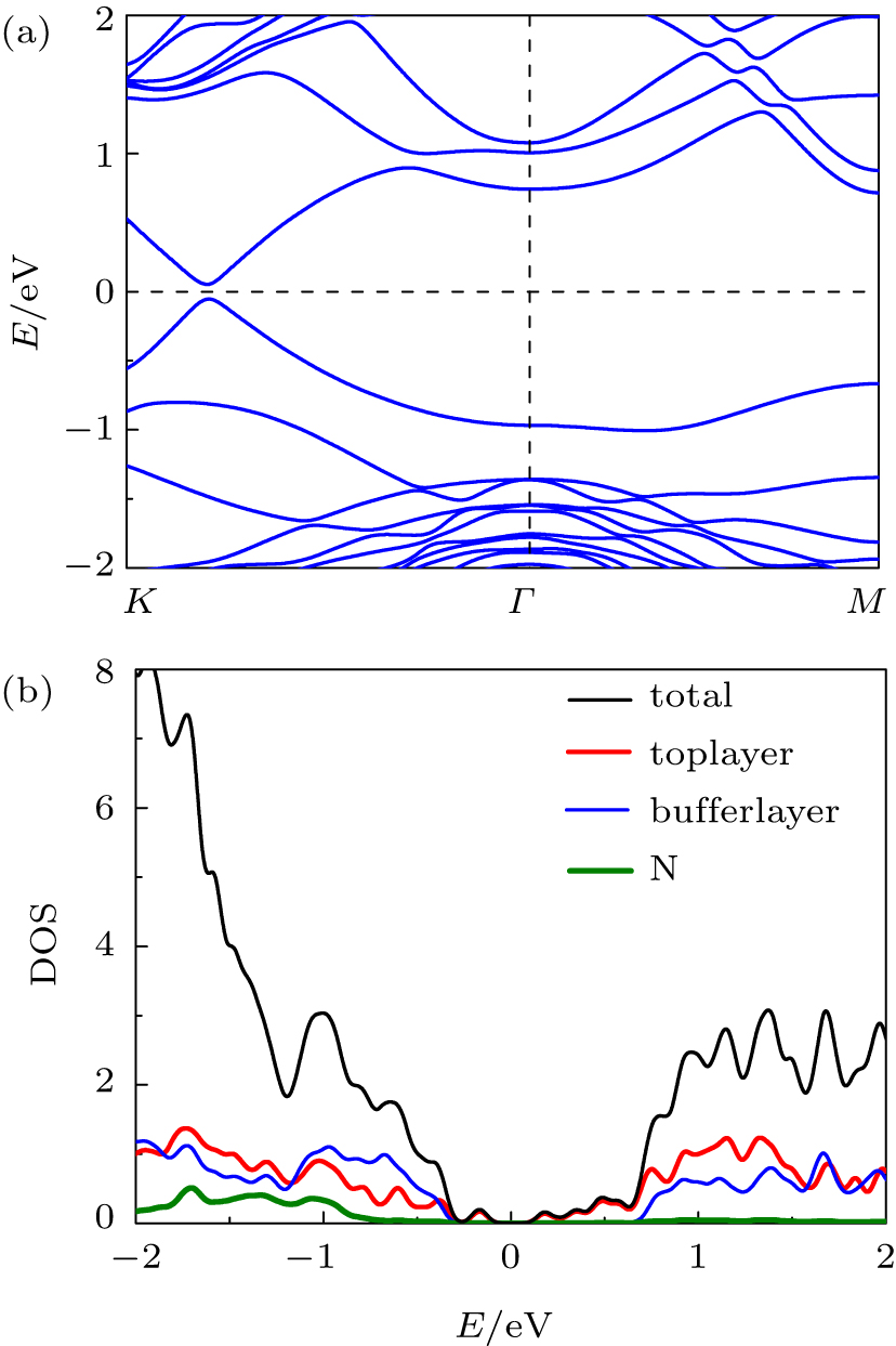
Fig. 6. (a) Band structure of bilayer graphene on Si-terminated SiC substrate with N intercalation. (b) The curves of total density of states and local density of states versus energy for top C layer, buffer layer, and N.
4. Conclusions

In this work, we investigate the band engineering and interface magnetism of epitaxial graphene on SiC(0001) by nonmetal atom doping. We find that its carrier type and density could be effectively manipulated by specific atoms (i.e., F, Cl, O, or N) decoration of the buffer layer. The fine tuning of the doping behavior from intrinsic n-type to charge neutrality to p-type and interface magnetism is achieved via increasing the adsorption concentration of F atoms on the buffer layer. Cl doping is similar to F doping. In addition, N decoration is also a good way to induce the metal-semiconductor transition with the Dirac point moving but not disappearing, while O modification can induce a p-type doping behavior. Our findings establish the potential for epitaxial graphene applications in nanoscale electronic and spintronic devices. Meanwhile, the mentioned ideas of intercalation in the graphene/substrate system can also be applied to similar systems such as silicone/substrate.

Reference
1 Ye W G Liu D Peng X F Dou W D 2013 Chin. Phys. B 22 117301
2 Zhao S Q Lv Y Lv W G Liang W J Wang E G 2014 Chin. Phys. B 23 067305
3 Si C Liu Z Duan W H Liu F 2013 Phys. Rev. Lett. 111 196802
4 Si C Duan W H Liu Z Liu F 2012 Phys. Rev. Lett. 109 226802
5 Quhe R Yuan Y Zheng J Wang Y Ni Z Shi J Yu D Yang J Lu J 2014 Sci. Rep. 4 5476
6 Abergel D S L Apalkov V Berashevich J Ziegler K Chakraborty T 2010 Adv. Phys. 59 261
7 Castro N A H Guinea F Peres N M R Novoselov K S Geim A K 2009 Rev. Mod. Phys. 81 109
8 Geim A K Novoselov K S 2007 Nat. Mater. 6 183
9 Yan Q Huang B Yu J Zheng F Zang J Wu J Gu B L Liu F Duan W 2007 Nano Lett. 7 1469
10 Emery J D Wheeler V H Johns J E McBriarty M E Detlefs B Hersam M C Gaskill D K Bedzyk M J 2014 Appl. Phys. Lett. 105 161602
11 Berger C Song Z Li T Li X Ogbazghi A Y Feng R Dai Z Marchenkov A N Conrad E H First P N de Heer W A 2004 J. Phys. Chem. B 108 19912
12 Berger C Song Z Li T Wu X Brown N Naud C Mayou D Li T Hass J Marchenkov A N Conrad E H Phillip N. First P N de Heer W A 2006 Science 312 1191
13 De Heer W A Berger C Wu X S First P N Conrad E H Li X B Li T B Sprinkle M Hass J Sadowski M L Potemski M Martinez G 2007 Solid State Commun. 143 92
14 Emtsev K V Bostwick A Horn K Jobst J Kellogg G L Ley L McChesney J L Ohta T Reshanov S A Rohrl J Rotenberg E Schmid A K Waldmann D Weber H B Seyller T 2009 Nat. Mater. 8 203
15 Riedl C Starke U Bernhardt J Franke M Heinz K 2007 Phys. Rev. B 76 245406
16 Chen W Xu H Liu L Gao X Qi D Peng G Tan S C Feng Y Loh K P Wee A T S 2005 Surf. Sci. 596 176
17 Brar V W Zhang Y Yayon Y Ohta T McChesney J L Bostwick A Rotenberg E Horn K Crommie M F 2007 Appl. Phys. Lett. 91 122102
18 Kim S Ihm J Choi H J Son Y W 2008 Phys. Rev. Lett. 100 176802
19 Varchon F Feng R Hass J Li X Nguyen B N Naud C Mallet P Veuillen J Y Berger C Conrad E H Magaud L 2007 Phys. Rev. Lett. 99 126805
20 Mattausch A Pankratov O 2007 Phys. Rev. Lett. 99 076802
21 Ohta T Bostwick A Seyller T Horn K Rotenberg E 2006 Science 313 951
22 Ohta T Bostwick A McChesney J L Seyller T Horn K Rotenberg E 2007 Phys. Rev. Lett. 98 206802
23 Riedl C Zakharov A A Starke U 2008 Appl. Phys. Lett. 93 033106
24 Bostwick A Ohta T Seyller T Horn K Rotenberg E 2007 Nat. Phys. 3 36
25 Wu Y Q Ye P D Capano M A Xuan Y Sui Y Qi M Cooper J A Shen T Pandey D Prakash G Reifenberger R 2008 Appl. Phys. Lett. 92 092102
26 Guo Y F Guo W L Chen C F 2009 Phys. Rev. B 80 085424
27 Zhou S Y Siegel D A Fedorov A V Lanzara A 2008 Phys. Rev. Lett. 101 086402
28 Chen W Chen S Qi D C Gao X Y Wee A T S 2007 J. Am. Chem. Soc. 129 10418
29 Coletti C Riedl C Lee D S Krauss B Patthey L von Klitzing K Smet J H Starke U 2010 Phys. Rev. B 81 235401
30 Gierz I Riedl C Starke U Ast C R Kern K 2008 Nano Lett. 8 4603
31 Huang B Si C Lee H Zhao L Wu J Gu B L Duan W 2010 Appl. Phys. Lett. 97 043115
32 Kim Y H Heben M J Zhang S B 2004 Phys. Rev. Lett. 92 176102
33 Orellana W Miwa R H Fazzio A 2003 Phys. Rev. Lett. 91 166802
34 Li L F Wang Y L Meng L Wu R T Gao H J 2013 Appl. Phys. Lett. 102 093106
35 Wang R Wang S Zhang D Li Z Fang Y Qiu X 2010 Acs Nano 5 408
36 Zhou S Y Gweon G H Fedorov A V First P N De Heer W A Lee D H Guinea F Neto A H C Lanzara A 2007 Nat. Mater. 6 916
37 Jayasekera T Kong B D Kim K W Buongiorno N M 2010 Phys. Rev. Lett. 104 146801
38 Huang B Xiang H J Wei S H 2011 Phys. Rev. B 83 161405
39 Si C Zhou G Li Y C Wu J Duan W H 2012 Appl. Phys. Lett. 100 103105
40 Kowalski G Tokarczyk M Dąbrowski P Ciepielewski P Możdżonek M Strupiński W Baranowski J M 2015 J. Appl. Phys. 117 105301
41 Giannozzi P Baroni S Bonini N Calandra M Car R Cavazzoni C Ceresoli D Chiarotti G L Cococcioni M Dabo I Dal Corso A de Gironcoli S Fabris S Fratesi G Gebauer R Gerstmann U Gougoussis C Kokalj A Lazzeri M Martin-Samos L Marzari N Mauri F Mazzarello R Paolini S Pasquarello A Paulatto L Sbraccia S Scandolo C Sclauzero G Seitsonen A P Smogunov A Umari P Wentzcovitch R M 2009 J. Phys.: Condens. Matter 21 395502
42 Boukhvalov D W Katsnelson M I 2009 J. Phys. Chem. C 113 14176