Li Pei, Guo Hong-Xia†, Guo Qi, Zhang Jin-Xin, Xiao Yao, Wei Ying, Cui Jiang-Wei, Wen Lin, Liu Mo-Han, Wang Xin. Single-event response of the SiGe HBT in TCAD simulations and laser microbeam experiment. Chinese Physics B, 24(8): 088502
Permissions
Single-event response of the SiGe HBT in TCAD simulations and laser microbeam experiment
Li Peia),b), Guo Hong-Xia†a),b),c), Guo Qia),b), Zhang Jin-Xind), Xiao Yaoc), Wei Yinga),b), Cui Jiang-Weia),b), Wen Lina),b), Liu Mo-Hana),b), Wang Xina),b)
Key Laboratory of Functional Materials and Devices for Special Environments of Chinese Academy of Sciences, Xinjiang Key Laboratory of Electronic Information Materials and Devices; Xinjiang Technical Institute of Physics & Chemistry, Chinese Academy of Sciences, Urumqi 830011, China
University of Chinese Academy of Sciences, Beijing 100049, China
Northwest Institution of Nuclear Technology, Xi’ an 710024, China
School of Science, Xi’an Jiaotong University, Xi’ an 710049, China
*Project supported by the National Natural Science Foundation of China (Grant No. 61274106).
Abstract
In this paper the single-event responses of the silicon germanium heterojunction bipolar transistors (SiGe HBTs) are investigated by TCAD simulations and laser microbeam experiment. A three-dimensional (3D) simulation model is established, the single event effect (SEE) simulation is further carried out on the basis of SiGe HBT devices, and then, together with the laser microbeam test, the charge collection behaviors are analyzed, including the single event transient (SET) induced transient terminal currents, and the sensitive area of SEE charge collection. The simulations and experimental results are discussed in detail and it is demonstrated that the nature of the current transient is controlled by the behaviors of the collector–substrate (C/S) junction and charge collection by sensitive electrodes, thereby giving out the sensitive area and electrode of SiGe HBT in SEE.
The present-day needs for electronic systems in the extreme environment of space present a host of challenges for satellite systems, space exploration platforms, and space-based remote imaging systems.[1, 2] SiGe heterojunction bipolar transistor (HBT) technology has emerged as a strong contender for high speed digital and mixed-signal applications because of its superior analog and RF performance, together with its complementary metal– oxide semiconductor (CMOS) integration capability.[3– 5] For space applications, SiGe HBTs have been demonstrated to be robust to both ionization and displacement damage without intentional hardening which, together with its performance metrics at cryogenic temperatures, makes them attractive for space applications.[6– 9]
However, recent testing and simulations have shown that SiGe HBT logic circuits could be vulnerable to the single event effect (SEE).[10– 13] Considerable charge collection occurs through the reverse-biased C/S junction, resulting in the single event upset (SEU) in fast SiGe HBT digital circuits for space applications.[14] To ensure the reliability of the SiGe HBTs and circuits used in spacecraft (especially outside of spacecraft), it is necessary to carry out in-depth research about SEE on SiGe HBT.
In this work we have built a simulation model and have carried out three-dimensional (3D) numerical simulations for SiGe HBT. In order to verify the simulation results, combining with the laser microbeam test for SiGe HBTs, we explore the SEE induced transient terminal currents, and analyze the sensitive areas of SEE charge collection. This paper provides a theoretical basis for practical applications of SiGe HBTs in space and further radiation hardening.
2. Three-dimensional numerical simulation
2.1. Device structure simulation
The simulation model of 3D SiGe HBT is structured based on device formation and process information, which was designed and fabricated by the Institute of Microelectronics, Tsinghua University. The 3D device simulations are performed by using Davinci, the rationality of the model is verified by comparing the data of simulation and test.[15] Figure 1 shows the 3D view of the entire constructed device, with the color indicating the material construction. The deep trench isolation (DTI) and shallow trend isolation (STI) are of SiO2 in light blue; while the substrate (S), collector (C), base (B), emitter (E) are all of silicon, which are led out by electrode in dark blue. In order to optimize the structure and save the computation time of the device models, we should create more grids in the SEE sensitive area. Figure 1 shows the outer shape of this 3D simulation model, whose external dimensions are 44 μ m× 36 μ m× 23.35 μ m.
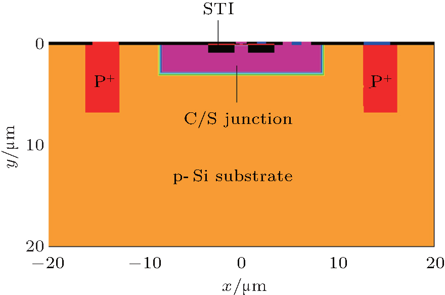
Figure 2 shows a cross section of z = 18 μ m obtained from the 3D simulation model, which is illustrated in Fig. 1. The active emitter area is formed by using STI around the base, and the outermost ring serves as a heavy boron-doped substrate contact. The other structures include an n-type collector with dimensions of 18 μ m× 3 μ m, together with a lightly doped p-type substrate, which is led out by the p+ reach through, forming a C/S junction.[16]
Fig. 2. Two-dimensional (2D) cross section of the SiGe HBT.
2.2. Device SET simulation
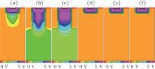
In the simulation, the substrate is biased at − 5 V and all other terminals are grounded. This represents the worst bias situation in the SiGe HBTs that would form a reverse-biased junction in a C/S junction. The ion used is 2100-MeV krypton with variable linear energy transfer (LET), and the strike position varies along the x-axis, with the y- axis is fixed in the center of the device. At each position, the strike simulated is a normal ion strike. A funneling behavior is evident by examining the potential contours in a series of plots from Fig. 3(a) to Fig. 3(f). At 3.0 ps (Fig. 3(a)), the potential begins to extend into the substrate due to the voltage drop along the charge column. At 13.0 ps (Fig. 3(b)), the potential along the ion track distorts to the substrate to form a funnel potential, and then spreads to the whole device. At 0.86 ns (Fig. 3(c)), the drift current starts to decrease as charges are swept from the depletion region, and then the depletion region is effectively restored and the charges that remain in the substrate are collected through diffusion. Finally, the potential contour returns to the original state at 9.0 ns (Fig. 3(d)).
Fig. 3. Electrostatic potentials of the SiGe HBT each as a function of time at (a) 0.003 ns, (b) 0.013 ns, (c) 0.86 ns, (d) 9 ns, (e) 60 ns, (f) 200 ns after an ion strike.
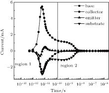
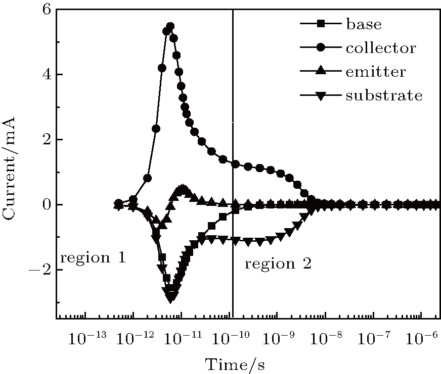
Figure 4 shows the transient waveforms of the base, emitter, collector, and substrate, each as a function of time, which can be broken into two distinct regions: region 1 and region 2.
Fig. 4. Transient terminal currents each as a function of time.
For region 1, as the ion passes through the semiconductor material, it leads to a dense concentration of electron– hole pairs through electron impact ionization. The charge carriers ionized within the depletion region of the C/S junction are separated by the electric field. Electrons are pulled out while holes are dumped into the lightly doped substrate, forming a funnel potential. During the time of region 1, the transient currents of the base and emitter terminals are relatively small, and the current of collector reaches up to 6 mA, as does the substrate.
For region 2, the excess holes begin to diffuse to the C/S junction and accumulate as they are pushed back by the electric field. There are almost no transient currents for the base and emitter during the time of region 2, while the currents of collector and substrate are symmetrically + 1.5 mA and − 1.5 mA, respectively. It can be concluded that the collector and substrate play a major role in charge collection.
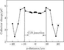
Because the 3D device simulation is time-consuming, it is not feasible to simulate all of the incident locations. Hence, some representative incident locations within the one and same cross section are chosen. Figure 5 presents the charges collected by collector as a function of x-coordinate of strike location. Sensitive regions are identified based on the analyses of the simulation results of different ion strike locations. For collector terminals, the C/S junction marks the edge for drastic charge collection change, outside which the charge collection decreases dramatically, hence the area of the C/S junction is determined to be the sensitive area for SiGe HBTs.
Fig. 5. Charges collected by collector as a function of the strike position.
3. Laser microbeam experiment
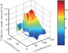
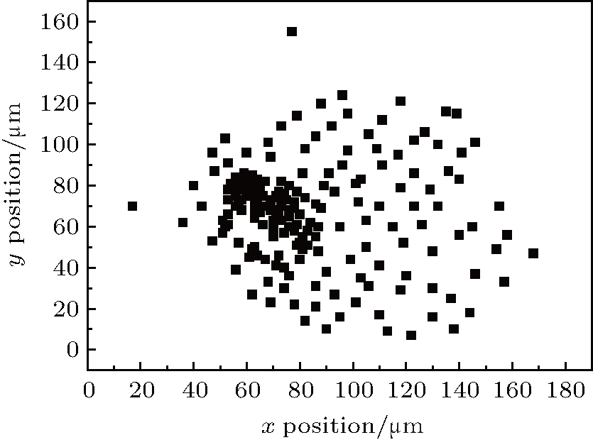
SEE simulation with laser microbeam is a simple and convenient method in SEE studies because it can focus into a small beam size and is capable of scanning sensitive junctions of devices.[17– 19] The SiGe HBT under test is loaded with a collector resistance of 50 Ω , and the wavelength of the laser microbeam is 1064 nm with a laser spot size of approximately 1.6 μ m in diameter. In order to access the device within sensitive regions, the laser spot must focus on the opening top metal layers in front of the device. Figure 6 shows the irradiation positions of laser microbeam, which are located uniformly on the x-axis between 0 and 180 μ m and between 0 and 160 μ m on the y-axis.
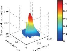
The SET pulses are captured at collector and base terminals by the digital sampling oscilloscope. Figures 7 and 8 show the plots of the collector peak currents and base peak currents each as a function of position, obtained from beam-induced peak currents on SiGe HBT. The active area is formed using STI in the base because the current of base is restricted by oxidation layer while the peak current of collector reaches up to 10 mA, which is 10 times the base peak current.
Fig. 8. Base terminal current transient peaks of the laser microbeam irradiation.
4. Analysis and discussion
The SiGe HBT under simulation and laser microbeam irradiation has a relatively large area of C/S junction, which plays very important role in SEE-induced charge collection, making the collector the most sensitive electrode. For the 3D numerical simulation, the ions penetrate SiGe HBT through its junctions and depletion layers, producing a track of ionization which is composed of electrons and holes. The presence of the ion track temporarily collapses the depletion layers into the track, distorting the potential of the depletion layer electric fields. This process results in a nesting of the funnel potential. Carries within the funnel drift quickly to the collector, and the current starts to decrease as charges are swept from the depletion region. The depletion region is then effectively restored and the charges that remain in the substrate are collected through diffusion. Figure 3 plots the electrostatic potential during the SEE, the potential contour is maximum for collector and substrate over the area of 18 μ m× 10 μ m, which is approximately the area of the CS junction; figure 4 shows the transient current for each terminal, and the current of collector reaches up to 6 mA, which is obviously the most sensitive electrode. As shown in Fig. 5, the charge collection of collector is nearly confined within the C/S junction, and drops off abruptly for ion strikes outside the C/S junction.
In the laser microbeam test, although the fitting for the simulation is not good for the numerical value of the currents, we can see that the simulated data follows the trend of the laser microbeam data. The transient currents are maximum for irradiation inside C/S junction and roll off for irradiation outside the C/S junction. Furthermore, the peak currents of collector reach up to 10 mA, which is 10 times the base peak current, confirming that the C/S junction and collector are the most sensitive area and electrode in SEE of SiGe HBT.
5. Conclusions
The results of simulation and laser microbeam test for SiGe HBT are discussed in detail and it is demonstrated that the C/S junction plays a major role in the charge collection induced by SEE, making the collector most sensitive electrode. The sensitive area for SiGe HBT is identified by simulation to agree with the transient current map obtained from the microbeam test, which approximately corresponds to the area of the C/S junction. This paper gives the sensitive area and electrode of SiGe HBT. In view of this result, much of the future work in the field of SiGe HBT in SEE should focus on radiation hardening of the C/S junction and collector.
SuttonA K, PrakashA P G, JunB, EnhaiZhao, BelliniM, PellishJ, DiestelhorstR M, CartsM A, PhanA, LadburyR, CresslerJ D, Marshall PW, MarshallC J, ReedR A, SchrimpfR D and FleetwoodD M2006IEEE Trans. Nucl. Sci. 533166DOI:10.1109/TNS.2006.885382[Cited within:1]
10
KrithivasanR, NiuG F, CresslerJ D, CurrieS M, FritzK E, ReedR AMarshallP W, RiggsP A, Rand allB A and GilbertB2003IEEE Trans. Nucl. Sci. 502126DOI:10.1109/TNS.2003.822094[Cited within:]
11
KrithivasanR, MarshallP W, NayeemM, SuttonA K, Wei-MinKuo, HaugerudB M, NajafizadehL, CresslerJ DCartsM AMarshallC JHansenD L, JobeK C M, McKayA L, NiuG F, ReedR A, Rand allB A, BurfieldC A, LindbergM D, GilbertB K and DanielE S2006IEEE Trans. Nucl. Sci. 533400DOI:10.1109/TNS.2006.885379[Cited within:1]
12
ReedR A, MarshallP W, PickelJ C, CartsM A, FodnessB, NiuG F, FritzK, VizkelethyG, DoddP E, IrwinT L, CresslerJ D, KrithivasanR, RiggsP A, PrairieJ, Rand allB A, GilbertB K and LabelK A2003IEEE Trans. Nucl. Sci. 502184DOI:10.1109/TNS.2003.821815[Cited within:1]
ZhangJ X, GuoH X, GuoQ, WenL, CuiJ W, XiS B, WangX and DengW2013Acta Phys. Sin. 62048501(in Chinese)DOI:10.7498/aps.62.048501[Cited within:1]
15
SunY B, FuJ, XuJ, WangY D, ZhouW, ZhangW, CuiJ, LiG Q, LiuZ H, YuY T, MaY Q, FengG Q and HanJ W2013Chin. Phys. B22056103DOI:10.1088/1674-1056/22/5/056103[Cited within:1]
... [1,2] SiGe heterojunction bipolar transistor (HBT) technology has emerged as a strong contender for high speed digital and mixed-signal applications because of its superior analog and RF performance, together with its complementary metal#cod#x02013 ...
1
2005
0.0
0.0
... [1,2] SiGe heterojunction bipolar transistor (HBT) technology has emerged as a strong contender for high speed digital and mixed-signal applications because of its superior analog and RF performance, together with its complementary metal#cod#x02013 ...
1
2006
0.0
0.0
... [3#cod#x02013 ...
1
1997
0.0
0.0
1
2003
0.0
0.0
... 5] For space applications, SiGe HBTs have been demonstrated to be robust to both ionization and displacement damage without intentional hardening which, together with its performance metrics at cryogenic temperatures, makes them attractive for space applications ...
1
1995
0.0
0.0
... [6#cod#x02013 ...
1
2003
0.0
0.0
1
2005
0.0
0.0
1
2006
0.0
0.0
... 9] ...
2003
1
2006
0.0
0.0
1
2003
0.0
0.0
1
2007
0.0
0.0
... 13] Considerable charge collection occurs through the reverse-biased C/S junction, resulting in the single event upset (SEU) in fast SiGe HBT digital circuits for space applications ...
1
2013
0.0
0.0
... [14] To ensure the reliability of the SiGe HBTs and circuits used in spacecraft (especially outside of spacecraft), it is necessary to carry out in-depth research about SEE on SiGe HBT ...
1
2013
0.0
0.0
... [15] Figure#cod#x000A0 ...
1
2013
0.0
0.0
... [16] ...
1
2008
0.0
0.0
... [17#cod#x02013 ...
1
2006
0.0
0.0
1
2014
0.0
0.0
... 19] The SiGe HBT under test is loaded with a collector resistance of 50#cod#x000A0 ...
Single-event response of the SiGe HBT in TCAD simulations and laser microbeam experiment
[Li Peia),b), Guo Hong-Xia†a),b),c), Guo Qia),b), Zhang Jin-Xind), Xiao Yaoc), Wei Yinga),b), Cui Jiang-Weia),b), Wen Lina),b), Liu Mo-Hana),b), Wang Xina),b)]


 , Guo Qi